EP1378814A2 - Output circuit device for clock signal distribution - Google Patents
Output circuit device for clock signal distribution Download PDFInfo
- Publication number
- EP1378814A2 EP1378814A2 EP02029039A EP02029039A EP1378814A2 EP 1378814 A2 EP1378814 A2 EP 1378814A2 EP 02029039 A EP02029039 A EP 02029039A EP 02029039 A EP02029039 A EP 02029039A EP 1378814 A2 EP1378814 A2 EP 1378814A2
- Authority
- EP
- European Patent Office
- Prior art keywords
- output circuit
- power supply
- transistor
- supply line
- output
- Prior art date
- Legal status (The legal status is an assumption and is not a legal conclusion. Google has not performed a legal analysis and makes no representation as to the accuracy of the status listed.)
- Withdrawn
Links
Images










Classifications
-
- H—ELECTRICITY
- H03—ELECTRONIC CIRCUITRY
- H03F—AMPLIFIERS
- H03F3/00—Amplifiers with only discharge tubes or only semiconductor devices as amplifying elements
- H03F3/45—Differential amplifiers
- H03F3/45071—Differential amplifiers with semiconductor devices only
- H03F3/45479—Differential amplifiers with semiconductor devices only characterised by the way of common mode signal rejection
- H03F3/45632—Differential amplifiers with semiconductor devices only characterised by the way of common mode signal rejection in differential amplifiers with FET transistors as the active amplifying circuit
- H03F3/45636—Differential amplifiers with semiconductor devices only characterised by the way of common mode signal rejection in differential amplifiers with FET transistors as the active amplifying circuit by using feedback means
- H03F3/45641—Measuring at the loading circuit of the differential amplifier
- H03F3/4565—Controlling the common source circuit of the differential amplifier
-
- H—ELECTRICITY
- H03—ELECTRONIC CIRCUITRY
- H03F—AMPLIFIERS
- H03F3/00—Amplifiers with only discharge tubes or only semiconductor devices as amplifying elements
- H03F3/45—Differential amplifiers
- H03F3/45071—Differential amplifiers with semiconductor devices only
- H03F3/45076—Differential amplifiers with semiconductor devices only characterised by the way of implementation of the active amplifying circuit in the differential amplifier
- H03F3/45179—Differential amplifiers with semiconductor devices only characterised by the way of implementation of the active amplifying circuit in the differential amplifier using MOSFET transistors as the active amplifying circuit
- H03F3/45183—Long tailed pairs
- H03F3/45192—Folded cascode stages
-
- H—ELECTRICITY
- H03—ELECTRONIC CIRCUITRY
- H03F—AMPLIFIERS
- H03F3/00—Amplifiers with only discharge tubes or only semiconductor devices as amplifying elements
- H03F3/45—Differential amplifiers
- H03F3/45071—Differential amplifiers with semiconductor devices only
- H03F3/45076—Differential amplifiers with semiconductor devices only characterised by the way of implementation of the active amplifying circuit in the differential amplifier
- H03F3/45179—Differential amplifiers with semiconductor devices only characterised by the way of implementation of the active amplifying circuit in the differential amplifier using MOSFET transistors as the active amplifying circuit
- H03F3/45237—Complementary long tailed pairs having parallel inputs and being supplied in series
-
- H—ELECTRICITY
- H03—ELECTRONIC CIRCUITRY
- H03F—AMPLIFIERS
- H03F3/00—Amplifiers with only discharge tubes or only semiconductor devices as amplifying elements
- H03F3/45—Differential amplifiers
- H03F3/45071—Differential amplifiers with semiconductor devices only
- H03F3/45479—Differential amplifiers with semiconductor devices only characterised by the way of common mode signal rejection
- H03F3/45632—Differential amplifiers with semiconductor devices only characterised by the way of common mode signal rejection in differential amplifiers with FET transistors as the active amplifying circuit
- H03F3/45636—Differential amplifiers with semiconductor devices only characterised by the way of common mode signal rejection in differential amplifiers with FET transistors as the active amplifying circuit by using feedback means
- H03F3/45641—Measuring at the loading circuit of the differential amplifier
- H03F3/45659—Controlling the loading circuit of the differential amplifier
-
- H—ELECTRICITY
- H03—ELECTRONIC CIRCUITRY
- H03F—AMPLIFIERS
- H03F2203/00—Indexing scheme relating to amplifiers with only discharge tubes or only semiconductor devices as amplifying elements covered by H03F3/00
- H03F2203/45—Indexing scheme relating to differential amplifiers
- H03F2203/45418—Indexing scheme relating to differential amplifiers the CMCL comprising a resistor addition circuit
-
- H—ELECTRICITY
- H03—ELECTRONIC CIRCUITRY
- H03F—AMPLIFIERS
- H03F2203/00—Indexing scheme relating to amplifiers with only discharge tubes or only semiconductor devices as amplifying elements covered by H03F3/00
- H03F2203/45—Indexing scheme relating to differential amplifiers
- H03F2203/45446—Indexing scheme relating to differential amplifiers there are two or more CMCLs
Definitions
- a technique for distributing a clock for accurate timing becomes important when it comes to increasing the speed of signal transmission within a cabinet or between circuit blocks or chips. That is, as the timing accuracy of the distributed clock directly affects the accuracy of receive timing and also the timing accuracy of a signal to be generated, a buffer that can minimize the occurrence of jitter must be used as a clock buffer for clock distribution. This applies not only to the clock distribution buffer, but also to various other output circuit devices that are required to operate at high speed with accurate timing.
- An object of the present invention is to provide an output circuit device that can operate at high speed with accurate timing by minimizing the occurrence of jitter.
- the low-pass filter circuit may comprise a filter resistor connected in series between the isolating transistor and the first or the second power supply line; and a filter capacitor one end of which is connected to a connection node between the isolating transistor and the filter resistor. A potential on the first or the second power supply line, whichever is not connected to the filter resistor, may be applied to the other end of the filter capacitor.
- an output circuit system having a plurality of output circuit devices, multi-phase clocks being transmitted through the plurality of output circuit devices, and phase spacing between multiple phases being maintained constant by adjusting the amount of delay in each of the output circuit devices in accordance with an output of a uniformity detection circuit that detects phase uniformity between the multi-phase clocks, wherein each of the output circuit devices comprises an amplifier circuit to which an input signal is supplied, wherein a common-mode voltage of the input signal is adjusted to a value substantially equal to a common-mode voltage of an output signal output from the amplifier circuit.
- a clock buffer (output circuit device) formed within an integrated circuit and, for example, is usually constructed using a full-swing output type inverter.
- Figure 2 is a circuit diagram showing another example of the prior art output circuit device, which is designed to process differential (complementary) signals. That is, in high-speed signal transmission, differential clock transmission is often used, and the example shown in Figure 2 concerns a clock buffer (output circuit device) for such differential clocks.
- the prior art output circuit device for differential clocks comprises two CMOS inverters 201, 203 and 202, 206, at which differential input clocks (input signals) in and /in, for example, are received, and cross-coupled nMOS transistors 204 and 205 provided in parallel with the nMOS transistors 203 and 206 in the respective CMOS inverters.
- differential output clocks (output signals) out and /out are derived in the form of the outputs of the inverters 202, 206 and 201, 203 respectively supplied with the input clocks /in and in.
- the output circuit device shown in Figure 1 or 2 is not limited to a clock buffer for clock signal distribution, the above deficiency becomes a problem in various other applications of the output circuit device.
- the output circuit device of the present invention also is not limited in application to a clock buffer, but can be applied extensively to various output circuit devices such as a buffer, driver, etc. used for signal transmission between a plurality of LSI chips or a plurality of devices or circuit blocks within a single chip or between a plurality of boards or cabinets.
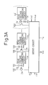
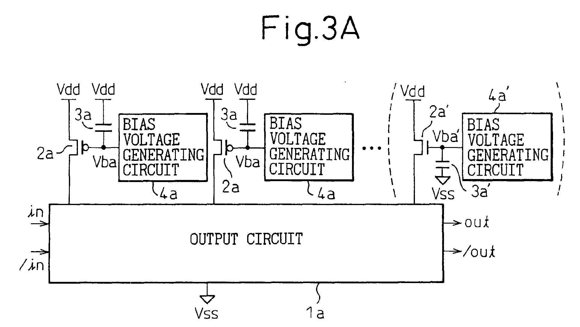
- Figures 3A and 3B are block circuit diagrams (part 1) schematically showing the basic functional configuration of the output circuit device according to the present invention.
- an isolating transistor is inserted between the high-level power supply line (Vdd) and output circuit (la), while in Figure 3B, the isolating transistor is inserted between the low-level power supply line (Vss) and output circuit (1b).
- reference numeral 1a is the output circuit (clock buffer circuit proper)
- 2a and 2a' are isolating transistors
- 3a and 3a' are capacitors (high-frequency component attenuating capacitors)
- 4a and 4a' are bias voltage generating circuits.
- the pMOS transistor 2a (or the nMOS transistor 2a') is inserted between the high-level power supply line (Vdd) and the output circuit 1a, and a constant-level control voltage (bias voltage) output from the bias voltage generating circuit 4a (4a') is applied to the gate of the transistor.
- the high-level supply voltage Vdd is, for example, 1.2 V
- the low-level supply voltage Vss is, for example, 0 V.
- the pMOS transistor (source-grounded pMOS transistor) 2a whose source is connected to the high-level power supply line, is supplied at its gate with a control voltage (bias voltage Vba), for example, of 1.0 V substantially equal to the drain potential, and functions as a current source.
- Vba bias voltage
- the capacitor 3a one terminal of which is connected to the gate of the pMOS transistor 2a, has its other terminal connected to the high-level power supply line (Vdd), and the high-frequency noise occurring in the potential difference between the gate of the transistor 2a and the high-level supply voltage Vdd isolated by the transistor 2a is reduced by a noise reduction filter circuit formed from the capacitor 3a.
- the nMOS transistor (source-follower connected nMOS transistor) 2a' whose drain is connected to the high-level power supply line, is supplied at its gate with a control voltage (bias voltage Vba') of a voltage level (for example, 1.0 V or 1.2 V) higher than the source potential by a value not smaller than the threshold voltage of that transistor, and isolates an internal circuit from the high-level power supply line.
- a control voltage bias voltage Vba'
- the capacitor 3a' one terminal of which is connected to the gate of the nMOS transistor 2a', has its other terminal connected to the low-level power supply line (Vss), and the high-frequency noise occurring in the potential difference between the gate of the transistor 2a' and the low-level supply voltage Vss on the side not isolated by the transistor 2a' is reduced by the capacitor 3a'.
- Vss low-level power supply line
- the output circuit 1a high-frequency components contained in the high-level supply voltage Vdd on the side isolated by the transistors 2a and 2a' can be attenuated.
- the isolating transistor between the high-level power supply line and the output circuit 1a can be inserted as needed by selecting either the pMOS transistor 2a or the nMOS transistor 2a'.
- the bias voltage generating circuits 4a and 4a' can each be configured, for example, as a circuit that will be described later with reference to Figure 10.
- the isolating transistors 2b and 2b' can be inserted between the output circuit 1b and the low-level power supply line (Vss), rather than inserting the isolating transistors 2a and 2a' between the output circuit 1a and the high-level power supply line (Vdd) as shown in Figure 3A above.
- the nMOS transistor 2b (or the pMOS transistor 2b') is inserted between the low-level power supply line (Vss) and the output circuit 1b, and a constant-level control voltage (bias voltage Vbb, (Vbb')) output from the bias voltage generating circuit 4b (4b') is applied to the gate of the transistor.
- Vss low-level power supply line
- Vbb' constant-level control voltage
- the nMOS transistor (source-grounded nMOS transistor) 2b whose source is connected to the low-level power supply line, functions as a current source, and the capacitor 3b, one terminal of which is connected to the gate of the nMOS transistor 2b, has its other terminal connected to the low-level power supply line (Vss).
- Vss low-level power supply line
- the pMOS transistor (source-follower pMOS transistor) 2b' whose drain is connected to the low-level power supply line, isolates an internal circuit from the high-level power supply line, and the capacitor 3b', one terminal of which is connected to the gate of the pMOS transistor 2b', has its other terminal connected to the high-level power supply line (Vdd); here, the high-frequency noise occurring in the potential difference between the gate of the transistor 2b' and the high-level supply voltage Vdd on the side not isolated by the transistor 2b' is reduced by a noise reduction filter circuit formed from the capacitor 3b'.
- Figure 4 is a block circuit diagram showing one example of the output circuit in the output circuit devices of Figures 3A and 3B, which is designed to reduce jitter by controlling the common mode.
- the output circuit 1 comprises a common-mode control circuit 11 and buffers 12 and 13.
- the common-mode control circuit 11 and the buffer 13 together function to cause the input common-mode voltage to coincide with the output common-mode voltage, and the outputs of the common-mode control circuit 11 are output via the buffer 12.
- the effect of the residual power supply variation described above can be reduced to a minimum by causing the common-mode voltage of the signals input to the circuit proper (output circuit 1a, 1b) to coincide with the steady-state common-mode voltage obtained in a condition where the effect of the power supply variation is reduced by isolation (that is, the voltage such that the common-mode voltage of the input signals in and /in equals the common-mode voltage of the output signals out and /out).
- isolation that is, the voltage such that the common-mode voltage of the input signals in and /in equals the common-mode voltage of the output signals out and /out.
- Figure 5 is a block circuit diagram (part 2) schematically showing the basic functional configuration of the output circuit device according to the present invention.
- reference numeral 51 is a differential skew correction circuit (duty detection and correction circuit), and 52 and 53 are buffers (buffer circuits).
- the circuit shown in Figure 5 can be applied, for example, as the output circuit 1a, 1b shown in Figure 3A, 3B.
- skew between the complementary (differential) clocks ⁇ 0 and ⁇ 2 and skew between ⁇ 1 and ⁇ 3, for example, are detected and fed back to the respective buffer circuits 52 and 53; by so doing, four-phase clocks ⁇ 0 to ⁇ 3 with improved phase uniformity can be generated.
- FIG. 6 is a block circuit diagram schematically showing a first embodiment of the output circuit device according to the present invention.
- reference numeral 1 is a circuit proper (output circuit)
- 21 to 24 are isolating pMOS transistors
- 31 and 32 are capacitors
- 5 is a common-mode feedback (CMFB) circuit.
- CMFB common-mode feedback
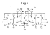
- Figure 7 is a circuit diagram showing one example of the common-mode feedback circuit 5 in the output circuit device of Figure 6.
- the common-mode feedback (CMFB) circuit 4 comprises pMOS transistors 511 to 516, capacitors 521 to 523, and nMOS transistors 531 to 537.
- Input signals c and d (the differential output signals out and /out of the output circuit device) are supplied to the nMOS transistor differential pair 533, 535; then, a difference voltage equal to the difference between the DC components of the input signals is generated by the capacitors 522 and 523, and the common-mode voltage of the output signals out and /out is fed back from the outputs (a and b) connected to the gates of the transistors 118 and 119, thereby compensating for the displacement of the duty.
- the common-mode feedback circuit 5 detects the common-mode voltage of the outputs of the output stage amplifier circuit (transistors 23, 24, 118, and 119), and feeds back current to the input nodes (the gates of the transistors 118 and 119) of the output amplifier circuit so that their values become equal.
- Figure 8 is a circuit diagram schematically showing a second embodiment of the output circuit device according to the present invention.
- the differential input signals in and /in are supplied to the gates of transistors 121, 123 and transistors 122, 125, respectively, each transistor pair forming a push-pull circuit (inverter).
- the common source of the pMOS transistors 121 and 122 is connected to the high-level power supply line (Vdd) via an isolating pMOS transistor 20 and a low-pass filter circuit 6, and the gate of the transistor 20 is connected to the drain of a pMOS transistor 61 (the source of the transistor 20) via a capacitor 30.
- the transistor 20 and the capacitor 30 correspond to the transistor 2a and the capacitor 3a, respectively, previously shown in Figure 3A.
- the capacitor 30, one terminal of which is connected to the gate of the transistor 20, has its other terminal connected to the high-level power supply line (Vdd) not directly, but via the pMOS transistor 61.
- the common-mode voltage of the output signals is compensated for by feeding back the output signals out and /out to the gate of a transistor 124 via resistors 127 and 126.
- the low-pass filter circuit 6 includes a capacitor (filter capacitor) 62 as well as the pMOS transistor (filter transistor) 61 whose gate is supplied with the low-level supply voltage Vss, and the high-frequency noise occurring in the high-level supply voltage Vdd is removed by the low-pass filter circuit 6; then, any remaining noise is isolated from the circuit proper 1 by the constant-current characteristic of the source-grounded pMOS transistor 20.
- Figure 9 is a circuit diagram schematically showing a third embodiment of the output circuit device according to the present invention.
- a resistor (filter resistor) 63 is used in place of the pMOS transistor 61 in the low-pass filter circuit 6. Otherwise, the configuration is the same as that of the second embodiment shown in Figure 8.
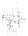
- the output circuit device of the fourth embodiment differs from the output circuit device of the second embodiment by the inclusion of a bias voltage generating circuit 4.
- the bias voltage generating circuit 4 comprises a capacitor 41, an nMOS transistor 42, and a pMOS transistor 43.
- the capacitor 41 and the nMOS transistor 42 are connected in series between the low-level power supply line (Vss) and the drain of the pMOS transistor (filter transistor) 61.
- the gate of the nMOS transistor 42 is supplied, for example, with an output voltage Vi from a buffer that is resistant to a variation in the high-level supply voltage Vdd.
- the pMOS transistor 43 has its source connected to the high-level power supply line (Vdd) and its gate and drain connected in common to the node between the capacitor 41 and the nMOS transistor 42, and the output bias voltage Vbp is taken from that node.
- the gate voltage of the pMOS gate-grounded transistor 20 is generated by receiving the current from the nMOS constant-current transistor 42 at the diode-connected pMOS transistor 43.
- the gate of the pMOS transistor 43 is connected to the capacitors 30 and 41 whose other ends are connected to the drain of the pMOS transistor 61.
- the high-frequency components of the voltage between the gate of the pMOS transistor 20 and the high-level power supply line (Vdd) are attenuated by the capacitors 30 and 41.
- the output circuit device of the fourth embodiment since high-frequency noise is not introduced in the gate-source voltage of the pMOS transistor 20, better isolation can be achieved and low jitter characteristics obtained.
- the circuit of the second embodiment shown in Figure 8 is used as the first stage amplifier, and a differential amplifier comprising nMOS transistors 23', 24', 120, 128, and 129 is used as the output stage amplifier which amplifies the outputs of the first stage amplifier. That is, the output stage amplifier comprises the differential pair drive transistors 128 and 129, source-follower loads (isolating nMOS transistors) 23' and 24', and current source 120.
- the isolating source-grounded pMOS transistor 20 and low-pass filter circuit 6 inserted between the first stage amplifier and the high-level power supply line (Vdd) and the capacitor 30 connected between the gate of the transistor 20 and the drain of the pMOS transistor 61 are provided for the first stage amplifier; with this arrangement, the high-frequency noise in the high-level supply voltage Vdd is sufficiently removed.
- the isolating source-grounded pMOS transistors 23 and 24 provided between the output stage amplifier (differential-pair transistors 128 and 129) and the high-level power supply line (Vdd) and the capacitor 32 connected between the high-level power supply line (Vdd) and the gates of the transistors 23 and 24 are provided for the output stage amplifier, to remove the high-frequency noise in the high-level supply voltage Vdd, while on the other hand, the high-frequency noise in the low-level supply voltage Vss is removed by the isolating source-follower nMOS transistors 23' and 24' provided between the high-level power supply line (Vdd) and the differential transistor pair 128, 129 and the capacitor 32' connected between the low-level power supply line (Vss) and the gates of the transistors 23' and 24'.
- the output circuit device of the fifth embodiment as the high-frequency noise in both the high-level supply voltage Vdd, and in the low-level supply voltage Vss, can be removed, and as the source-follower nMOS transistors 23' and 24' are used as the differential amplifier in the amplifier stage, a low impedance load is achieved and high-speed, small-amplitude clocks can be generated.
- Figure 12 is a circuit diagram schematically showing a sixth embodiment of the output circuit device according to the present invention.
- the output circuit device of the sixth embodiment is similar in circuit configuration to the output circuit device of the second embodiment.
- the output circuit device of the sixth embodiment differs in that the back-gate BG potential (well potential) of the pMOS transistors (differential pair) 121 and 122 is not the high-level supply voltage Vdd, but is the drain voltage of the isolating pMOS transistor 20, that is, the voltage Vdd' obtained by removing the high-frequency noise from the high-level supply voltage Vdd.
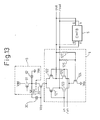
- the common-mode feedback circuit 5 comprises, as shown in Figure 14, a replica circuit 50, which generates a common-mode reference voltage Vref, and amplifiers 70 and 80, which control the common-mode voltage of the output signals by comparing the voltage levels of the output signals out and /out with the reference voltage Vref.
- the replica circuit 50 has a configuration (circuit proper 501, isolating source-grounded pMOS transistor 520, capacitor 530, and filter circuit 506) essentially similar to the output circuit device (circuit proper 1, isolating source-grounded pMOS transistor 20, capacitor 30, and filter circuit 6). However, in the replica circuit 50, the gates of the transistors 5121 to 5125 and the drains of the transistors 5121 to 5123 and 6125 are connected together to a common node, and the reference voltage Vref is taken from that common node.
- the filter circuit 506 in the replica circuit 50 comprises a pMOS transistor 561 and a capacitor 562, similarly to the filter circuit 6.
- each amplifier 70 (80) comprises: an amplifier circuit 740 (840), which differentially amplifies the reference voltage Vref and a signal e (f) input via a low-pass filter comprising a resistor 741 (841) and a capacitor 742 (842); a filter circuit 706 (806) having a pMOS transistor 761 (861) and a capacitor 762 (862); an isolating source-grounded pMOS transistor 720 (820); a capacitor 730 (830); and nMOS drive transistor 710 (810).
- an amplifier circuit 740 (840) which differentially amplifies the reference voltage Vref and a signal e (f) input via a low-pass filter comprising a resistor 741 (841) and a capacitor 742 (842); a filter circuit 706 (806) having a pMOS transistor 761 (861) and a capacitor 762 (862); an isolating source-grounded pMOS transistor 720 (820); a capacitor 730 (830); and
- Figure 15 is a circuit diagram showing one example of the differential amplifier circuit 740 (840) in the common-mode feedback circuit of Figure 14.
- the differential amplifier circuit 740 comprises pMOS differential-pair transistors 741 and 742, to which the reference voltage Vref and the signal e input via the low-pass filter, respectively, are applied, and nMOS load transistors 743 and 744.
- the reference voltage Vref generated by the replica circuit 50 having a configuration (circuit proper 501, isolating source-grounded pMOS transistor 520, capacitor 530, and filter circuit 506) essentially similar to the output circuit device (circuit proper 1, isolating source-grounded pMOS transistor 20, capacitor 30, and filter circuit 6), is compared with the common mode of the output signals out and /out (e and f), and the results of the comparisons are fed back (g and h) to the output signals, so that control can be performed so as to cause the common-mode voltage level of the output signals out and /out to substantially coincide with the reference voltage Vref.
- the common-mode feedback is performed only on the output side of the output circuit device, it is possible to construct the amplifier stage as a single stage amplifier.
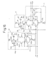
- Figure 16 is a circuit diagram schematically showing an eighth embodiment of the output circuit device according to the present invention.
- a circuit (common-mode voltage generating circuit) similar to the replica circuit 50 in Figure 14 is provided for a single-stage amplifier circuit similar to the one in the second embodiment of Figure 8, and the input signals in and /in are supplied via resistors 511 and 512 to the gates of the differential-pair transistors 5121, 5122 and 5123, 5125, that is, the differential input signals in and /in are terminated in the common-mode voltage generating circuit 50 via the resistors 511 and 512.
- the common-mode voltage of the input signals in and /in is brought close in value to the output voltage of the common-mode voltage generating circuit 50 (the reference voltage Vref of the replica circuit).
- the output circuit device of the eighth embodiment is superior in terms of the frequency characteristic of the common-mode voltage variation suppression circuit. That is, while the common-mode feedback necessarily entails a delay through the feedback amplifier circuit, in the eighth embodiment the fluctuation in delay associated with the feedback can be eliminated because the common-mode voltage is controlled by a termination that does not involve feedback.
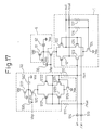
- Figure 17 is a circuit diagram schematically showing a ninth embodiment of the output circuit device according to the present invention.
- the output circuit device of the ninth embodiment differs from the output circuit device of the eighth embodiment by the inclusion of capacitors 513 and 514 for AC coupling on the input side.
- nodes Nin and /Nin on the AC-coupled input side of the output circuit are supplied with a bias voltage (reference voltage Vref) from the common-mode voltage generating circuit (replica circuit) 50 shown in Figure 16.
- the output circuit device of the ninth embodiment has the advantage that, when the output circuit device is applied, for example, to a configuration where the signals propagate through multi-stage clock buffers, variations in the common-mode voltage can be completely suppressed.
- Figure 18 is a circuit diagram showing one example of the differential skew correction circuit 51 in the output circuit device of Figure 5 as a 10th embodiment according to the present invention, in which a duty (duty cycle) detection circuit and correction circuit (feedback nMOS transistors 5009 to 5020) are provided at the output of the buffer.
- a duty (duty cycle) detection circuit and correction circuit feedback nMOS transistors 5009 to 5020
- the circuit shown in Figure 5 can be applied, for example, as the output circuit 1a, 1b shown in Figure 3A, 3B, and the embodiment shows an example as applied to a clock buffer for transmitting four-phase clocks ⁇ 0 to ⁇ 3 spaced 90° apart in phase.
- a complementary (differential) pair of clocks ⁇ 0 (clock of 0° phase: i) and ⁇ 2 (clock of 180° phase: j) and a complementary pair of clocks ⁇ 1 (clock of 90° phase: k) and ⁇ 3 (clock of 270° phase: 1) are input to the differential skew correction circuit 51, and skew between ⁇ 0 and ⁇ 2. and skew between ⁇ 1 and ⁇ 3 are detected and fed back to the respective buffer circuits 52 and 53, thereby generating four-phase clocks ⁇ 0 to ⁇ 3 having improved phase uniformity.
- the differential skew correction circuit 51 comprises pMOS transistors 5001 to 5008, nMOS transistors 5009 to 5026, and capacitors 5027 to 5029.
- the differential inputs i and j (clocks ⁇ 0 and ⁇ 2) are supplied to the gates of the differential-pair transistors 5009 and 5010, 5011 and 5012, and 5020 and 5019, respectively, while the differential inputs k and 1 (clocks ⁇ 1 and ⁇ 3) are supplied to the gates of the differential-pair transistors 5013 and 5014, 5015 and 5016, and 5017 and 5018, respectively.
- signals m and n created by combinations of the capacitors 5027 to 5029 connected to signal lines L1 and L2 are output via the pMOS transistors 5005, 5006 and 5008, 5007, respectively, whose gates are connected to the respective signal lines L1 and L2.
- the buffer circuits 52 and 53 By controlling the buffer circuits 52 and 53 using these signals m and n, the duty between the respective clock pairs ⁇ 0, ⁇ 2 and ⁇ 1, ⁇ 3 is adjusted to or near 50%, while performing feedback so as to maintain the 90° phase difference between the respective four clocks ⁇ 0 to ⁇ 3, thereby outputting the four-phase clocks ⁇ 0 to ⁇ 3 having accurate phase spacing.
- the output circuit device of the 10th embodiment is preferable as a clock buffer to be used, for example, in a timing generating circuit that requires multi-phase clocks with accurate phase spacing.
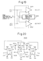
- Figure 19 is a circuit diagram showing one example of the buffer circuit 52 in the output circuit device of Figure 5 as an 11th embodiment according to the present invention.
- the complementary (differential) pair of clocks ⁇ 0 (clock of 0° phase) and ⁇ 2 (clock of 180° phase), for example, are supplied to buffers 5201 and 5202 as well as to a duty cycle correction circuit 5203.
- the duty cycle correction circuit 5203 detects and compares the duty cycles (high level "H” and low level “L” periods) of the clocks ⁇ 0 and ⁇ 2, and supplies control signals p and q to the buffers 5201 and 5202 to apply corrections so that the duty cycles of the clocks ⁇ 0 and ⁇ 2 become equal to each other.
- the output (m) of the earlier described differential skew correction circuit 51 is supplied to the buffers 5201 and 5202, and the skew between the input clocks ⁇ 0 and ⁇ 2, detected and corrected by the differential skew correction circuit 51, is fed back to the buffers 5201 and 5202, to generate the clocks ⁇ 0 and ⁇ 2 having improved phase uniformity.
- Figure 20 is a circuit diagram showing one example of the duty cycle correction circuit 5203 in the buffer circuit of Figure 19.
- the duty cycle correction circuit 5203 comprises pMOS transistors 5231 to 5236, nMOS transistors 5237 to 5243, and capacitors 5244 to 5246.
- the duty cycle correction circuit 5203 detects and corrects the skew between the input clocks ⁇ 0 and ⁇ 2, and feeds back the control signal p (q). to the buffer 5201 (5202) to generate the clocks ⁇ 0 and ⁇ 2 with improved phase uniformity.
- the duty of each clock ⁇ 0, ⁇ 2 can be adjusted to or near 50% at all times, which serves to prevent a pulse from gradually diminishing in width and eventually disappearing while the clock is propagating, for example, through multi-stage clock buffers.
- the output circuit device of the present invention is not limited to a clock buffer to be used for clock distribution, but can be applied to various buffers that require high-speed operation with accurate timing. Furthermore, the output circuit device of the present invention is applicable not only to two-phase (differential) and four-phase signals, but also to eight-phase or other multi-phase signals (for example, multi-phase clocks); for example, an output circuit system can be constructed that maintains constant phase spacing between multiple phases by adjusting the amount of delay in each output circuit device in accordance with an output of a uniformity detection circuit that detects phase uniformity between multi-phase clocks.
- an output circuit device can be provided that can minimize jitter and can operate at high speed with accurate timing.
Landscapes
- Engineering & Computer Science (AREA)
- Power Engineering (AREA)
- Logic Circuits (AREA)
- Amplifiers (AREA)
Abstract
Description
Claims (28)
- An output circuit device comprising an output circuit connected between a first power supply line and a second power supply line via a control circuit having at least one isolating transistor, wherein
a control voltage held at a constant level is applied to a control electrode of said isolating transistor, and
said control voltage is a voltage at a level that works to attenuate high-frequency components contained in a voltage supplied from said first or said second power supply line. - The output circuit device as claimed in claim 1, wherein said control circuit comprises a high-frequency component attenuating capacitor one end of which is connected to the control electrode of said isolating transistor.
- The output circuit device as claimed in claim 2, wherein
said isolating transistor is a source-grounded MOS transistor, and
the other end of said high-frequency component attenuating capacitor is connected to a source side of said first or said second power supply line whichever is connected to said source-grounded MOS transistor. - The output circuit device as claimed in claim 3, wherein
said isolating transistor is a pMOS transistor whose source is connected to said first power supply line, and whose drain is connected to said output circuit, and
the other end of said high-frequency component attenuating capacitor is connected to said first power supply line. - The output circuit device as claimed in claim 3, wherein
said isolating transistor is an nMOS transistor whose source is connected to said second power supply line, and whose drain is connected to said output circuit, and
the other end of said high-frequency component attenuating capacitor is connected to said second power supply line. - The output circuit device as claimed in claim 2, wherein
said isolating transistor is a source-follower connected MOS transistor, and
the other end of said high-frequency component attenuating capacitor is connected either to said first or said second power supply line, whichever is not connected to said source-follower connected MOS transistor, or to a node having a prescribed potential difference relative to said power supply line not connected to said source-follower connected MOS transistor. - The output circuit device as claimed in claim 6, wherein
said isolating transistor is an nMOS transistor whose source is connected to said output circuit, and whose drain is connected to said first power supply line, and
the other end of said high-frequency component attenuating capacitor is connected to said second power supply line. - The output circuit device as claimed in claim 6, wherein
said isolating transistor is a pMOS transistor whose source is connected to said output circuit, and whose drain is connected to said second power supply line, and
the other end of said high-frequency component attenuating capacitor is connected to said first power supply line. - The output circuit device as claimed in claim 1, wherein
said control voltage is generated through a noise reduction filter circuit, and
said noise reduction filter circuit attenuates the high-frequency components contained in the voltage supplied from said first or said second power supply line whichever is connected to said isolating MOS transistor. - The output circuit device as claimed in claim 1, wherein
said output circuit comprises a pair of inverters amplifying differential signals, and
a voltage passed through said control circuit is applied to a back gate of a transistor forming each of said inverters. - The output circuit device as claimed in claim 10, wherein a well of each pMOS transistor forming said pair of inverters is connected to the source of said pMOS transistor.
- The output circuit device as claimed in claim 1, wherein said isolating transistor is provided on at least one side of either between said output circuit and said first power supply line or between said output circuit and said second power supply line.
- The output circuit device as claimed in claim 12, wherein said isolating transistor is provided on both sides of between said output circuit and said first power supply line and between said output circuit and said second power supply line.
- The output circuit device as claimed in claim 1, further comprising a low-pass filter circuit provided in series to said isolating transistor.
- The output circuit device as claimed in claim 14, wherein said low-pass filter circuit comprises:a filter transistor connected in series between said isolating transistor and said first or said second power supply line; anda filter capacitor one end of which is connected to a connection node between said isolating transistor and said filter transistor.
- The output circuit device as claimed in claim 15, wherein a potential on said first or said second power supply line, whichever is not connected to said filter transistor, is applied to a control electrode of said filter transistor as well as to the other end of said filter capacitor.
- The output circuit device as claimed in claim 14, wherein said low-pass filter circuit comprises:a filter resistor connected in series between said isolating transistor and said first or said second'power supply line; anda filter capacitor one end of which is connected to a connection node between said isolating transistor and said filter resistor.
- The output circuit device as claimed in claim 17, wherein a potential on said first or said second power supply line, whichever is not connected to said filter resistor, is applied to the other end of said filter capacitor.
- The output circuit device as claimed in claim 1, further comprising:a duty detection circuit detecting an output duty of said output circuit; anda duty adjusting circuit adjusting the output duty of said output circuit in accordance with said detected duty, and wherein the ratio of said output duty is controlled to approximately 50%.
- The output circuit device as claimed in claim 1, wherein said output circuit device is a clock buffer used for clock signal distribution.
- An output circuit device comprising an amplifier circuit to which an input signal is supplied, wherein a common-mode voltage of said input signal is adjusted to a value substantially equal to a common-mode voltage of an output signal output from said amplifier circuit.
- The output circuit device as claimed in claim 21, wherein the adjustment of the common-mode voltage of said input signal is performed by a common-mode feedback circuit provided on an output side of a transmitting circuit that transmits signals to said output circuit device.
- The output circuit device as claimed in claim 21, wherein the adjustment of the common-mode voltage of said input signal is performed by terminating said input signal with a power supply that is provided on an input side of said output circuit device and that generates a common-mode voltage of a prescribed level.
- The output circuit device as claimed in claim 21, wherein the adjustment of the common-mode voltage of said input signal is performed by capacitively coupling said input signal with said amplifier circuit and by supplying a DC potential, after said capacitive coupling, to a power supply that is provided on an input side of said output circuit device and that generates a common-mode voltage of a prescribed level.
- The output circuit device as claimed in claim 21, further comprising:a duty detection circuit detecting an output duty of said output circuit; anda duty adjusting circuit adjusting the output duty of said output circuit in accordance with said detected duty, and wherein the ratio of said output duty is controlled to approximately 50%.
- The output circuit device as claimed in claim 21, wherein said output circuit device is a clock buffer used for clock signal distribution.
- An output circuit system having a plurality of output circuit devices, multi-phase clocks being transmitted through said plurality of output circuit devices, and phase spacing between multiple phases being maintained constant by adjusting the amount of delay in each of said output circuit devices in accordance with an output of a uniformity detection circuit that detects phase uniformity between said multi-phase clocks, wherein each of said output circuit devices comprises an output circuit connected between a first power supply line and a second power supply line via a control circuit having at least one isolating transistor, wherein
a control voltage held at a constant level is applied to a control electrode of said isolating transistor, and
said control voltage is a voltage at a level that works to attenuate high-frequency components contained in a voltage supplied from said first or said second power supply line. - An output circuit system having a plurality of output circuit devices, multi-phase clocks being transmitted through said plurality of output circuit devices, and phase spacing between multiple phases being maintained constant by adjusting the amount of delay in each of said output circuit devices in accordance with an output of a uniformity detection circuit that detects phase uniformity between said multi-phase clocks, wherein each of said output circuit devices comprises an amplifier circuit to which an input signal is supplied, wherein a common-mode voltage of said input signal is adjusted to a value substantially equal to a common-mode voltage of an output signal output from said amplifier circuit.
Applications Claiming Priority (2)
| Application Number | Priority Date | Filing Date | Title |
|---|---|---|---|
| JP2002153885 | 2002-05-28 | ||
| JP2002153885A JP3935777B2 (en) | 2002-05-28 | 2002-05-28 | Output circuit device |
Publications (2)
| Publication Number | Publication Date |
|---|---|
| EP1378814A2 true EP1378814A2 (en) | 2004-01-07 |
| EP1378814A3 EP1378814A3 (en) | 2006-11-02 |
Family
ID=29561333
Family Applications (1)
| Application Number | Title | Priority Date | Filing Date |
|---|---|---|---|
| EP02029039A Withdrawn EP1378814A3 (en) | 2002-05-28 | 2002-12-27 | Output circuit device for clock signal distribution |
Country Status (3)
| Country | Link |
|---|---|
| US (2) | US6812777B2 (en) |
| EP (1) | EP1378814A3 (en) |
| JP (1) | JP3935777B2 (en) |
Cited By (1)
| Publication number | Priority date | Publication date | Assignee | Title |
|---|---|---|---|---|
| GB2400997A (en) * | 2003-03-28 | 2004-10-27 | Nec Electronics Corp | A CMOS differential amplifier with a common-mode feedback circuit acting on the output nodes. |
Families Citing this family (40)
| Publication number | Priority date | Publication date | Assignee | Title |
|---|---|---|---|---|
| US7031858B1 (en) * | 2003-05-16 | 2006-04-18 | Silicon Image, Inc. | Method and circuit for DC measurement of phase uniformity of multi-phase clocks |
| JP3948446B2 (en) | 2003-09-03 | 2007-07-25 | セイコーエプソン株式会社 | Semiconductor device |
| JP2005322105A (en) * | 2004-05-11 | 2005-11-17 | Seiko Instruments Inc | Constant voltage output circuit |
| JP4504108B2 (en) * | 2004-06-15 | 2010-07-14 | 富士通セミコンダクター株式会社 | Reset circuit |
| US7227402B2 (en) * | 2004-08-23 | 2007-06-05 | Micron Technology, Inc. | System and method for controlling input buffer biasing current |
| KR20060040267A (en) * | 2004-11-05 | 2006-05-10 | 삼성전자주식회사 | Differential Amplifier with High Voltage Gain and Stable Common Mode Output Voltage |
| US7352204B2 (en) * | 2005-05-13 | 2008-04-01 | Warpspeed Chips, Llc | Automatic skew correction for differential signals |
| JP4923442B2 (en) * | 2005-06-06 | 2012-04-25 | ソニー株式会社 | Differential signal transmission circuit and differential signal transmission device |
| KR20060131321A (en) * | 2005-06-15 | 2006-12-20 | 삼성전자주식회사 | High Efficiency Power Amplifier with Precision Duty Cycle |
| JP4391976B2 (en) * | 2005-09-16 | 2009-12-24 | 富士通株式会社 | Clock distribution circuit |
| KR100808076B1 (en) * | 2005-09-16 | 2008-03-03 | 후지쯔 가부시끼가이샤 | Clock distribution circuit |
| JP5025171B2 (en) * | 2005-09-29 | 2012-09-12 | エスケーハイニックス株式会社 | Differential amplifier |
| US7737731B1 (en) | 2005-10-20 | 2010-06-15 | Marvell International Ltd. | High data rate envelope detector for high speed optical storage application |
| JP4752465B2 (en) * | 2005-11-25 | 2011-08-17 | パナソニック電工株式会社 | Wireless transmission circuit and wireless transmission device |
| US7623050B2 (en) * | 2005-12-13 | 2009-11-24 | Broadcom Corporation | Digital calibration loop for an analog to digital converter |
| US7812746B2 (en) * | 2005-12-14 | 2010-10-12 | Broadcom Corporation | Variable gain and multiplexing in a digital calibration for an analog-to-digital converter |
| US7843368B2 (en) * | 2005-12-14 | 2010-11-30 | Broadcom Corporation | Programmable settling for high speed analog to digital converter |
| US7456764B2 (en) * | 2005-12-14 | 2008-11-25 | Broadcom Corporation | Analog to digital converter with dynamic power configuration |
| US7466249B2 (en) * | 2005-12-14 | 2008-12-16 | Broadcom Corporation | System and method for common mode calibration in an analog to digital converter |
| US20070159224A1 (en) * | 2005-12-21 | 2007-07-12 | Amar Dwarka | Duty-cycle correction circuit for differential clocking |
| US7489176B2 (en) * | 2006-04-28 | 2009-02-10 | Rambus Inc. | Clock distribution circuit |
| EP2039004A2 (en) * | 2006-06-30 | 2009-03-25 | Nxp B.V. | Circuit for detecting the duty cycle of clock signals |
| KR100763849B1 (en) * | 2006-08-10 | 2007-10-05 | 삼성전자주식회사 | A phase correction circuit for reducing phase skew between multi phase clock signals, a method thereof, and a semiconductor device comprising the circuit |
| US8027377B2 (en) | 2006-08-14 | 2011-09-27 | Intersil Americas Inc. | Differential driver with common-mode voltage tracking and method |
| JP4412507B2 (en) | 2007-10-03 | 2010-02-10 | Necエレクトロニクス株式会社 | Semiconductor circuit |
| US20090245813A1 (en) * | 2008-03-31 | 2009-10-01 | Kitel Technologies Llc | Modulator driver with multi-channel active alignment |
| US7920027B2 (en) * | 2008-04-07 | 2011-04-05 | Qualcomm Incorporated | Amplifier design with biasing and power control aspects |
| KR101068037B1 (en) * | 2008-11-25 | 2011-09-28 | (주)락싸 | Sensor circuit |
| JP4783418B2 (en) * | 2008-11-27 | 2011-09-28 | 富士通株式会社 | Duty correction circuit and duty correction method |
| US8040159B1 (en) * | 2010-03-23 | 2011-10-18 | Lattice Semiconductor Corporation | Comparator with jitter mitigation |
| JP5917858B2 (en) * | 2011-08-29 | 2016-05-18 | ルネサスエレクトロニクス株式会社 | Semiconductor integrated circuit device |
| RU2592719C2 (en) * | 2012-03-16 | 2016-07-27 | Интел Корпорейшн | Reference voltage generator with low impedance |
| US8798127B2 (en) * | 2012-11-15 | 2014-08-05 | Altera Corporation | Apparatus and methods for adaptive receiver delay equalization |
| JP2015012479A (en) | 2013-06-28 | 2015-01-19 | 富士通株式会社 | Electronic component, information processing device, and electronic component control method |
| JP2015149669A (en) * | 2014-02-07 | 2015-08-20 | 富士通株式会社 | Clock control circuit, receiver and communication device |
| US9525391B2 (en) | 2014-03-05 | 2016-12-20 | Mediatek Singapore Pte. Ltd. | Fully differential class A/AB amplifier and method thereof |
| US10044362B2 (en) | 2014-06-19 | 2018-08-07 | Texas Instruments Incorporated | Complementary current reusing preamp for operational amplifier |
| KR102668197B1 (en) * | 2017-02-08 | 2024-05-23 | 에스케이하이닉스 주식회사 | Semiconductor Apparatus |
| TWI736121B (en) * | 2020-02-03 | 2021-08-11 | 瑞昱半導體股份有限公司 | Duty cycle corrector |
| US11942960B2 (en) * | 2022-01-31 | 2024-03-26 | Analog Devices, Inc. | ADC with precision reference power saving mode |
Family Cites Families (9)
| Publication number | Priority date | Publication date | Assignee | Title |
|---|---|---|---|---|
| US5739681A (en) * | 1992-02-07 | 1998-04-14 | Crosspoint Solutions, Inc. | Voltage regulator with high gain cascode current mirror |
| DE69534839D1 (en) * | 1995-07-31 | 2006-05-04 | Sgs Thomson Microelectronics | Circuit for controlled independent consumption of stored inductive energy of a plurality of inductive loads |
| US6362682B2 (en) * | 1998-06-30 | 2002-03-26 | Agere Systems Guardian Corp. | Common-mode feedback circuit and method |
| US6191622B1 (en) * | 1998-10-01 | 2001-02-20 | Ati International Srl | Time interleaved common mode feedback circuit with process compensated bias |
| US6529070B1 (en) * | 1999-10-25 | 2003-03-04 | Texas Instruments Incorporated | Low-voltage, broadband operational amplifier |
| FR2811090B1 (en) * | 2000-06-28 | 2002-10-11 | St Microelectronics Sa | INTEGRATION OF A VOLTAGE REGULATOR |
| JP2002083930A (en) * | 2000-09-08 | 2002-03-22 | Fujitsu Ltd | Semiconductor device |
| US6509727B2 (en) * | 2000-11-24 | 2003-01-21 | Texas Instruments Incorporated | Linear regulator enhancement technique |
| US6650191B2 (en) * | 2001-09-07 | 2003-11-18 | Texas Instruments Incorporated | Low jitter ring oscillator architecture |
-
2002
- 2002-05-28 JP JP2002153885A patent/JP3935777B2/en not_active Expired - Fee Related
- 2002-12-26 US US10/328,002 patent/US6812777B2/en not_active Expired - Lifetime
- 2002-12-27 EP EP02029039A patent/EP1378814A3/en not_active Withdrawn
-
2004
- 2004-09-22 US US10/945,965 patent/US6963237B2/en not_active Expired - Lifetime
Cited By (3)
| Publication number | Priority date | Publication date | Assignee | Title |
|---|---|---|---|---|
| GB2400997A (en) * | 2003-03-28 | 2004-10-27 | Nec Electronics Corp | A CMOS differential amplifier with a common-mode feedback circuit acting on the output nodes. |
| GB2400997B (en) * | 2003-03-28 | 2005-05-25 | Nec Electronics Corp | Voltage control circuit for common mode voltage and method for controlling the same |
| US7126425B2 (en) | 2003-03-28 | 2006-10-24 | Nec Electronics Corporation | Voltage control circuit for common mode voltage and method for controlling the same |
Also Published As
| Publication number | Publication date |
|---|---|
| US20030222705A1 (en) | 2003-12-04 |
| US6812777B2 (en) | 2004-11-02 |
| JP2003347920A (en) | 2003-12-05 |
| EP1378814A3 (en) | 2006-11-02 |
| JP3935777B2 (en) | 2007-06-27 |
| US6963237B2 (en) | 2005-11-08 |
| US20050035789A1 (en) | 2005-02-17 |
Similar Documents
| Publication | Publication Date | Title |
|---|---|---|
| US6963237B2 (en) | Output circuit device for clock signal distribution in high-speed signal transmission | |
| US7098699B2 (en) | Buffer circuit device supplying a common mode voltage applicable to a next-stage circuit receiving output signals of the buffer circuit device | |
| US7233172B2 (en) | Differential amplifier circuit capable of accurately amplifying even high-speeded signal of small amplitude | |
| US6535040B2 (en) | Duty cycle correction circuits that reduce distortion caused by mismatched transistor pairs | |
| US6169424B1 (en) | Self-biasing sense amplifier | |
| US7768328B2 (en) | Semiconductor circuit | |
| US20030204767A1 (en) | Clock recovery circuit for high-speed data signal transmission | |
| US8022728B2 (en) | Common-mode voltage controller | |
| US20050200411A1 (en) | Differential amplifier without common mode feedback | |
| US11936386B2 (en) | Clock transfer circuit including a semiconductor device for compensating delay fluctuation | |
| US5221910A (en) | Single-pin amplifier in integrated circuit form | |
| US7741873B2 (en) | Receiver circuitry for receiving reduced swing signals from a channel | |
| US7298201B2 (en) | Clock buffer circuit having predetermined gain with bias circuit thereof | |
| US7038520B2 (en) | Timing signal generating circuit and receiver circuit designed to speed up signal transmission | |
| US8072268B2 (en) | Operational amplifier | |
| US6452453B1 (en) | Constant-current generator, differential amplifier, and semiconductor integrated circuit | |
| EP1550149B1 (en) | Constant delay zero standby differential logic receiver and method | |
| US7187196B2 (en) | Low rise/fall skewed input buffer compensating process variation | |
| US7057438B2 (en) | Output circuit and semiconductor integrated circuit incorporating it therein | |
| EP1764670B1 (en) | Clock distribution circuit | |
| US7071772B2 (en) | Differential amplifier | |
| EP1699135A2 (en) | Low amplitude differential output circuit and serial transmission interface using the same | |
| KR100417857B1 (en) | Circuit for input receiver in rambus dram | |
| JPH11330867A (en) | Bias circuit for CMOS amplifier and method for adjusting channel length of MOS transistor in bias circuit |
Legal Events
| Date | Code | Title | Description |
|---|---|---|---|
| PUAI | Public reference made under article 153(3) epc to a published international application that has entered the european phase |
Free format text: ORIGINAL CODE: 0009012 |
|
| AK | Designated contracting states |
Kind code of ref document: A2 Designated state(s): AT BE BG CH CY CZ DE DK EE ES FI FR GB GR IE IT LI LU MC NL PT SE SI SK TR |
|
| AX | Request for extension of the european patent |
Extension state: AL LT LV MK RO |
|
| RIC1 | Information provided on ipc code assigned before grant |
Ipc: G06F 1/04 20060101ALI20060719BHEP Ipc: G06F 1/10 20060101AFI20031114BHEP |
|
| PUAL | Search report despatched |
Free format text: ORIGINAL CODE: 0009013 |
|
| AK | Designated contracting states |
Kind code of ref document: A3 Designated state(s): AT BE BG CH CY CZ DE DK EE ES FI FR GB GR IE IT LI LU MC NL PT SE SI SK TR |
|
| AX | Request for extension of the european patent |
Extension state: AL LT LV MK RO |
|
| 17P | Request for examination filed |
Effective date: 20070226 |
|
| AKX | Designation fees paid |
Designated state(s): DE FR GB |
|
| 17Q | First examination report despatched |
Effective date: 20080305 |
|
| STAA | Information on the status of an ep patent application or granted ep patent |
Free format text: STATUS: THE APPLICATION IS DEEMED TO BE WITHDRAWN |
|
| 18D | Application deemed to be withdrawn |
Effective date: 20160701 |