EP1376861B1 - Device for converting a differential signal to a single signal - Google Patents
Device for converting a differential signal to a single signal Download PDFInfo
- Publication number
- EP1376861B1 EP1376861B1 EP03076840A EP03076840A EP1376861B1 EP 1376861 B1 EP1376861 B1 EP 1376861B1 EP 03076840 A EP03076840 A EP 03076840A EP 03076840 A EP03076840 A EP 03076840A EP 1376861 B1 EP1376861 B1 EP 1376861B1
- Authority
- EP
- European Patent Office
- Prior art keywords
- terminals
- drivable
- rout
- transistors
- terminal
- Prior art date
- Legal status (The legal status is an assumption and is not a legal conclusion. Google has not performed a legal analysis and makes no representation as to the accuracy of the status listed.)
- Expired - Lifetime
Links
- 101100112673 Rattus norvegicus Ccnd2 gene Proteins 0.000 claims description 8
- 230000007423 decrease Effects 0.000 description 2
- 238000006243 chemical reaction Methods 0.000 description 1
- 238000002955 isolation Methods 0.000 description 1
Images


Classifications
-
- H—ELECTRICITY
- H03—ELECTRONIC CIRCUITRY
- H03F—AMPLIFIERS
- H03F3/00—Amplifiers with only discharge tubes or only semiconductor devices as amplifying elements
- H03F3/45—Differential amplifiers
- H03F3/45071—Differential amplifiers with semiconductor devices only
- H03F3/45076—Differential amplifiers with semiconductor devices only characterised by the way of implementation of the active amplifying circuit in the differential amplifier
- H03F3/4508—Differential amplifiers with semiconductor devices only characterised by the way of implementation of the active amplifying circuit in the differential amplifier using bipolar transistors as the active amplifying circuit
- H03F3/45085—Long tailed pairs
-
- H—ELECTRICITY
- H03—ELECTRONIC CIRCUITRY
- H03F—AMPLIFIERS
- H03F3/00—Amplifiers with only discharge tubes or only semiconductor devices as amplifying elements
- H03F3/45—Differential amplifiers
- H03F3/45071—Differential amplifiers with semiconductor devices only
- H03F3/45076—Differential amplifiers with semiconductor devices only characterised by the way of implementation of the active amplifying circuit in the differential amplifier
- H03F3/4508—Differential amplifiers with semiconductor devices only characterised by the way of implementation of the active amplifying circuit in the differential amplifier using bipolar transistors as the active amplifying circuit
- H03F3/45085—Long tailed pairs
- H03F3/45089—Non-folded cascode stages
-
- H—ELECTRICITY
- H03—ELECTRONIC CIRCUITRY
- H03F—AMPLIFIERS
- H03F2203/00—Indexing scheme relating to amplifiers with only discharge tubes or only semiconductor devices as amplifying elements covered by H03F3/00
- H03F2203/45—Indexing scheme relating to differential amplifiers
- H03F2203/45296—Indexing scheme relating to differential amplifiers the AAC comprising one or more discrete capacitive elements, e.g. a transistor coupled as capacitor
-
- H—ELECTRICITY
- H03—ELECTRONIC CIRCUITRY
- H03F—AMPLIFIERS
- H03F2203/00—Indexing scheme relating to amplifiers with only discharge tubes or only semiconductor devices as amplifying elements covered by H03F3/00
- H03F2203/45—Indexing scheme relating to differential amplifiers
- H03F2203/45392—Indexing scheme relating to differential amplifiers the AAC comprising resistors in the source circuit of the AAC before the common source coupling
-
- H—ELECTRICITY
- H03—ELECTRONIC CIRCUITRY
- H03F—AMPLIFIERS
- H03F2203/00—Indexing scheme relating to amplifiers with only discharge tubes or only semiconductor devices as amplifying elements covered by H03F3/00
- H03F2203/45—Indexing scheme relating to differential amplifiers
- H03F2203/45394—Indexing scheme relating to differential amplifiers the AAC of the dif amp comprising FETs whose sources are not coupled, i.e. the AAC being a pseudo-differential amplifier
-
- H—ELECTRICITY
- H03—ELECTRONIC CIRCUITRY
- H03F—AMPLIFIERS
- H03F2203/00—Indexing scheme relating to amplifiers with only discharge tubes or only semiconductor devices as amplifying elements covered by H03F3/00
- H03F2203/45—Indexing scheme relating to differential amplifiers
- H03F2203/45702—Indexing scheme relating to differential amplifiers the LC comprising two resistors
Definitions
- the present invention refers to a device for converting a differential signal to a single signal.
- radio frequency field devices adapted to convert a differential signal to a single signal are generally employed. This occurs since in the integrated circuits, which typically have a single output signal, it is necessary to work with differential signals since the single signal circuit structures show isolation problems making them not usable in the case of high frequency operations.
- a device used for converting a differential signal to a single signal is constituted by a pair of transistors arranged in a differential stage configuration and with an active load (see e.g. US 5406219 ).
- this solution is used at frequencies lower than the radio frequencies and has the further disadvantage to be used for a lot of open loop applications.
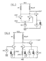
- the device more used is a differential stage of transistors with a resistive load and a single output, as shown in Figure 1 .
- the transistors Q10 and Q11 are arranged in a supply path between the voltages VDD and VEE.
- An input differential voltage Vin1 0 is present at the base terminals and the collector terminals of the transistors Q10 and Q11 are connected with the terminals of two resistors R10, R11 connected with the supply voltage VDD.
- the collector terminal of the transistor Q11 is the output terminal OUT10 of the device.
- the capacity CE decreases the common mode rejection at radio frequency.
- this object is obtained by means of a device for converting a differential signal to a single signal, said device comprising at least one pair of transistors having equal transconductance gain, which are arranged according a differential stage configuration and which have said differential signal in input at the drivable terminals, first non drivable terminals coupled respectively to first terminals of a first and a second passive elements having second terminals connected with a first supply voltage, second non drivable terminals coupled to a second supply voltage, said first supply voltage being higher than the second supply voltage and the first terminal of the second passive element being the output terminal of the device, characterized by comprising a further transistor having a first non drivable terminal connected with the output terminal of the device, a second non drivable terminal coupled with said second supply voltage and the drivable terminal connected with the first terminal of the first passive element, said further transistor having such a transconductance gain that the product of said transconductance gain by said first passive element is unitary.
- the present invention it is possible to form a device for converting a differential signal to a single signal which has a gain higher than the known devices and is not sensitive to the common mode voltages.
- the device comprises two transistors Q1 and Q2, for example bipolar transistors, which are arranged according a differential stage configuration with the emitter terminals connected to each other and connected with a current generator IEE connected with a supply voltage VEE, with the collector terminals connected respectively with two resistors R1 and Rout which are connected with the supply voltage VDD, and with the two base terminals driven by two voltage signals Vin1 and Vin2 which represent the input differential signal.
- transistors Q1 and Q2 for example bipolar transistors, which are arranged according a differential stage configuration with the emitter terminals connected to each other and connected with a current generator IEE connected with a supply voltage VEE, with the collector terminals connected respectively with two resistors R1 and Rout which are connected with the supply voltage VDD, and with the two base terminals driven by two voltage signals Vin1 and Vin2 which represent the input differential signal.
- Another transistor Q3 in such case a bipolar transistor, has the collector terminal connected with the collector terminal of the transistor Q2 which is even the output terminal OUT of the device, the base terminal coupled with the collector terminal of the transistor Q1 and the emitter terminal connected with a current generator I and with a capacity C which are together connected with the supply voltage VEE.
- the transistor Q3 has such a transconductance gain gm3 that the product of the same by the resistor R1 is unitary.
- the transconductance gains gm1 and gm2 of the transistors Q1 and Q2 are equal and preferably the resistors Rout and R1 have equal value.
- gm1 the transconductance gain of the transistor Q1
- gm3 the transconductance gain of the transistor Q3.
- FIG 5 a variant of the device in Figure 3 according to a variant of the embodiment is described wherein the differential stage constituted by the transistors Q1 and Q2 are made cascode by adding the transistors Q4 and Q5 arranged between the resistors R1 and Rout and the collector terminal of the transistors Q1 and Q2. More in detail the transistors Q4 and Q5 have the emitter terminals connected with the collector terminals of the transistors Q1 and Q2, the collector terminals connected with the resistors R1 and Rout and at the base terminals a biasing voltage Vb is present which allows a gain of the circuit higher than that of the circuit in Figure 3 .
Landscapes
- Engineering & Computer Science (AREA)
- Power Engineering (AREA)
- Amplifiers (AREA)
Description
- The present invention refers to a device for converting a differential signal to a single signal.
- In the radio frequency field devices adapted to convert a differential signal to a single signal are generally employed. This occurs since in the integrated circuits, which typically have a single output signal, it is necessary to work with differential signals since the single signal circuit structures show isolation problems making them not usable in the case of high frequency operations.
- A device used for converting a differential signal to a single signal is constituted by a pair of transistors arranged in a differential stage configuration and with an active load (see e.g.
US 5406219 ). However this solution is used at frequencies lower than the radio frequencies and has the further disadvantage to be used for a lot of open loop applications. - The device more used is a differential stage of transistors with a resistive load and a single output, as shown in
Figure 1 . The transistors Q10 and Q11 are arranged in a supply path between the voltages VDD and VEE. An input differential voltage Vin1 0 is present at the base terminals and the collector terminals of the transistors Q10 and Q11 are connected with the terminals of two resistors R10, R11 connected with the supply voltage VDD. The collector terminal of the transistor Q11 is the output terminal OUT10 of the device. In such case an output voltage Vout10 will be obtained which is given by VoutlO=-gm*R10/2, where gm is the transconductance gain for the transistors Q10 and Q11; the conversion from the differential signal to single signal decreases the gain of the circuit. - The circuit in
Figure 2 is the circuit equivalent of the circuit inFigure 1 for the calculation of the common mode gain for small signal, where ZEE is the equivalent impedance of the current generator IEE which, at high frequency, is given by ZEE=2REE/(1+ j2πCE*REE). It is obtained:
- Therefore the capacity CE decreases the common mode rejection at radio frequency.
- In view of the art described, it is an object to present invention to provide a device for converting a differential signal to a single signal which overcomes the aforementioned drawbacks.
- According to the present invention, this object is obtained by means of a device for converting a differential signal to a single signal, said device comprising at least one pair of transistors having equal transconductance gain, which are arranged according a differential stage configuration and which have said differential signal in input at the drivable terminals, first non drivable terminals coupled respectively to first terminals of a first and a second passive elements having second terminals connected with a first supply voltage, second non drivable terminals coupled to a second supply voltage, said first supply voltage being higher than the second supply voltage and the first terminal of the second passive element being the output terminal of the device, characterized by comprising a further transistor having a first non drivable terminal connected with the output terminal of the device, a second non drivable terminal coupled with said second supply voltage and the drivable terminal connected with the first terminal of the first passive element, said further transistor having such a transconductance gain that the product of said transconductance gain by said first passive element is unitary.
- Thanks to the present invention it is possible to form a device for converting a differential signal to a single signal which has a gain higher than the known devices and is not sensitive to the common mode voltages.
- The features and the advantages of the present invention will be made evident by the following detailed description of embodiments thereof, shown as not limiting examples in the annexed drawings, wherein:
-
Figure 1 is a circuit scheme of a device for converting a differential signal to a single signal according to prior art; -
Figure 2 is a circuit used for the calculation of the common mode gain of the circuit inFigure 1 ; -
Figure 3 is a circuit scheme of a device for converting a differential signal to a single signal according to an embodiment of the invention; -
Figure 4 is a circuit used for the calculation of the common mode gain of the circuit inFigure 3 ; -
Figure 5 is a variant of the device inFigure 3 according a variant of the embodiment. - Referring to
Figure 3 a device for converting a differential signal to a single signal according to an embodiment of the invention is described. The device comprises two transistors Q1 and Q2, for example bipolar transistors, which are arranged according a differential stage configuration with the emitter terminals connected to each other and connected with a current generator IEE connected with a supply voltage VEE, with the collector terminals connected respectively with two resistors R1 and Rout which are connected with the supply voltage VDD, and with the two base terminals driven by two voltage signals Vin1 and Vin2 which represent the input differential signal. Another transistor Q3, in such case a bipolar transistor, has the collector terminal connected with the collector terminal of the transistor Q2 which is even the output terminal OUT of the device, the base terminal coupled with the collector terminal of the transistor Q1 and the emitter terminal connected with a current generator I and with a capacity C which are together connected with the supply voltage VEE. The transistor Q3 has such a transconductance gain gm3 that the product of the same by the resistor R1 is unitary. The transconductance gains gm1 and gm2 of the transistors Q1 and Q2 are equal and preferably the resistors Rout and R1 have equal value. - It is possible to calculate the gain between an output voltage Vout at the terminal OUT and a input voltage Vin1, Vin2 by making the other input voltage equal to zero. Therefore by making Vin2=0 it occurs that:

- By making Vin1=0 it occurs:

Figure 3 and by keeping this condition it is obtained that the gain Av of the same device is given by:
- In
figure 4 a circuit scheme similar to the scheme inFigure 3 is described for calculating the common mode gain. Considering that the common mode voltages Vc are given by Vc=(Vin1+Vin2) and the impedance ZEE is the equivalent impedance of the current generator IEE that, at high frequency, is given by ZEE=2REE/(1+j2πCE*REE), it is obtained:

- In
figure 5 a variant of the device inFigure 3 according to a variant of the embodiment is described wherein the differential stage constituted by the transistors Q1 and Q2 are made cascode by adding the transistors Q4 and Q5 arranged between the resistors R1 and Rout and the collector terminal of the transistors Q1 and Q2. More in detail the transistors Q4 and Q5 have the emitter terminals connected with the collector terminals of the transistors Q1 and Q2, the collector terminals connected with the resistors R1 and Rout and at the base terminals a biasing voltage Vb is present which allows a gain of the circuit higher than that of the circuit inFigure 3 .
Claims (7)
- Device for converting a differential signal (Vin1, Vin2) to a single signal (Vout), said device comprising at least one pair of transistors (Q1, Q2) having equal transconductance gain (gm), which are arranged according a differential stage configuration and which have said differential signal (Vin1, Vin2) in input at the drivable terminals, first non drivable terminals coupled respectively to first terminals of a first (R1) and a second (Rout) passive elements having second terminals connected with a first supply voltage (VDD), second non drivable terminals coupled to a second supply voltage (VEE), said first supply voltage (VDD) being higher than the second supply voltage (VEE) and the first terminal of the second passive element (Rout) being the output terminal (OUT) of the device, characterized by comprising a further transistor (Q3) having a first non drivable terminal connected with the output terminal (OUT) of the device, a second non drivable terminal coupled with said second supply voltage (VEE) and the drivable terminal connected with the first terminal of the first passive element (R1), said further transistor (Q3) having such a transconductance gain (gm3) that the product of said transconductance gain (gm3) by said first passive element (R1) is unitary.
- Device according to claim 1, characterized in that said pair of transistors (Q1, Q2) is a pair of bipolar transistors having equal input resistance.
- Device according to claim 1, characterized in that said further transistor (Q3) is a common emitter bipolar transistor.
- Device according to claim 1, characterized in that said first non drivable terminals are connected with said first terminals of said first (R1) and second (Rout) passive elements.
- Device according to claim 1, characterized in that said first (R1) and second (Rout) passive elements have equal value.
- Device according to claim 1, characterized by comprising a further pair of transistors (Q4, Q5) which has first non drivable terminals connected with first non drivable terminals of said pair of transistors (Q1, Q2), second non drivable terminals connected with said first terminals of the passive elements (R1, Rout), drivable terminals connected with a biasing voltage (Vb).
- Device according to claim 1, characterized in that said passive elements (R1, Rout) are resistors.
Applications Claiming Priority (2)
| Application Number | Priority Date | Filing Date | Title |
|---|---|---|---|
| IT2002MI001336A ITMI20021336A1 (en) | 2002-06-17 | 2002-06-17 | DEVICE FOR THE CONVERSION OF A DIFFERENTIAL SIGNAL INTO A SINGLE SIGNAL |
| ITMI20021336 | 2002-06-17 |
Publications (3)
| Publication Number | Publication Date |
|---|---|
| EP1376861A2 EP1376861A2 (en) | 2004-01-02 |
| EP1376861A3 EP1376861A3 (en) | 2004-05-19 |
| EP1376861B1 true EP1376861B1 (en) | 2009-03-25 |
Family
ID=29717158
Family Applications (1)
| Application Number | Title | Priority Date | Filing Date |
|---|---|---|---|
| EP03076840A Expired - Lifetime EP1376861B1 (en) | 2002-06-17 | 2003-06-13 | Device for converting a differential signal to a single signal |
Country Status (4)
| Country | Link |
|---|---|
| US (1) | US6909328B2 (en) |
| EP (1) | EP1376861B1 (en) |
| DE (1) | DE60326789D1 (en) |
| IT (1) | ITMI20021336A1 (en) |
Families Citing this family (2)
| Publication number | Priority date | Publication date | Assignee | Title |
|---|---|---|---|---|
| US8103224B1 (en) * | 2006-09-19 | 2012-01-24 | Rf Micro Devices, Inc. | Method and apparatus for the integration of a high efficiency power amplifier with an integrated transceiver for wireless communication |
| US7902923B2 (en) * | 2009-03-19 | 2011-03-08 | Qualcomm, Incorporated | Common-gate common-source amplifier |
Family Cites Families (6)
| Publication number | Priority date | Publication date | Assignee | Title |
|---|---|---|---|---|
| US4607232A (en) * | 1985-04-01 | 1986-08-19 | Raytheon Company | Low voltage amplifier circuit |
| AU601336B2 (en) * | 1988-08-05 | 1990-09-06 | Matsushita Electric Industrial Co., Ltd. | Amplifier |
| US4959622A (en) * | 1989-08-31 | 1990-09-25 | Delco Electronics Corporation | Operational amplifier with precise bias current control |
| FR2684252A1 (en) * | 1991-11-22 | 1993-05-28 | Thomson Composants Militaires | ULTRA-FAST DIFFERENTIAL AMPLIFIER. |
| US5406219A (en) * | 1993-02-10 | 1995-04-11 | Brooktree Corporation | Differential-to-single-ended converter |
| US5327100A (en) * | 1993-03-01 | 1994-07-05 | Motorola, Inc. | Negative slew rate enhancement circuit for an operational amplifier |
-
2002
- 2002-06-17 IT IT2002MI001336A patent/ITMI20021336A1/en unknown
-
2003
- 2003-06-13 EP EP03076840A patent/EP1376861B1/en not_active Expired - Lifetime
- 2003-06-13 DE DE60326789T patent/DE60326789D1/en not_active Expired - Lifetime
- 2003-06-17 US US10/463,010 patent/US6909328B2/en not_active Expired - Lifetime
Also Published As
| Publication number | Publication date |
|---|---|
| US6909328B2 (en) | 2005-06-21 |
| EP1376861A2 (en) | 2004-01-02 |
| US20030231063A1 (en) | 2003-12-18 |
| DE60326789D1 (en) | 2009-05-07 |
| EP1376861A3 (en) | 2004-05-19 |
| ITMI20021336A1 (en) | 2003-12-17 |
Similar Documents
| Publication | Publication Date | Title |
|---|---|---|
| US20030141935A1 (en) | High speed differential to single-ended converter | |
| JP3088262B2 (en) | Low distortion differential amplifier circuit | |
| US6710654B2 (en) | Bipolar class AB folded cascode operational amplifier for high-speed applications | |
| EP3439174A1 (en) | Plural feedback loops instrumentation folded cascode amplifier | |
| US6545502B1 (en) | High frequency MOS fixed and variable gain amplifiers | |
| US20140022015A1 (en) | Multiple-output transconductance amplifier based instrumentation amplifier | |
| EP0853379A1 (en) | Low noise amplifier | |
| US6531920B1 (en) | Differential amplifier circuit | |
| US6344762B1 (en) | Bias circuit for a low voltage differential circuit | |
| EP1376861A2 (en) | Device for converting a differential signal to a single signal | |
| CN100578917C (en) | Gain amplifier circuit for minimizing miller effect | |
| US6570427B2 (en) | Variable transconductance amplifier | |
| US10199995B2 (en) | Programmable amplifier circuit capable of providing large or larger resistance for feedback path of its amplifier | |
| US5973539A (en) | Mixer circuit for mixing two signals having mutually different frequencies | |
| JPH09331220A (en) | Gain variable amplifier | |
| EP1684418B1 (en) | Differential to single-ended converter | |
| EP1676362B1 (en) | Electronic circuit for amplification of a bipolar signal | |
| US7567125B2 (en) | Differential amplifier with multiple signal gains and wide dynamic range | |
| US7019590B1 (en) | Self-stabilizing differential load circuit with well controlled impedance | |
| US9985589B2 (en) | System and method for improving total harmonic distortion of an amplifier | |
| JPH10247831A (en) | Amplifier circuit | |
| US20030107437A1 (en) | High speed linear variable gain amplifier architecture | |
| JP2000114929A (en) | Impedance circuit and phase shifter | |
| KR19990030039A (en) | Device for converting symmetric signals into asymmetric signals | |
| US8933754B2 (en) | Linear differential amplifier with high input impedance |
Legal Events
| Date | Code | Title | Description |
|---|---|---|---|
| PUAI | Public reference made under article 153(3) epc to a published international application that has entered the european phase |
Free format text: ORIGINAL CODE: 0009012 |
|
| AK | Designated contracting states |
Kind code of ref document: A2 Designated state(s): AT BE BG CH CY CZ DE DK EE ES FI FR GB GR HU IE IT LI LU MC NL PT RO SE SI SK TR |
|
| AX | Request for extension of the european patent |
Extension state: AL LT LV MK |
|
| PUAL | Search report despatched |
Free format text: ORIGINAL CODE: 0009013 |
|
| AK | Designated contracting states |
Kind code of ref document: A3 Designated state(s): AT BE BG CH CY CZ DE DK EE ES FI FR GB GR HU IE IT LI LU MC NL PT RO SE SI SK TR |
|
| AX | Request for extension of the european patent |
Extension state: AL LT LV MK |
|
| 17P | Request for examination filed |
Effective date: 20041110 |
|
| AKX | Designation fees paid |
Designated state(s): DE FR GB IT |
|
| GRAP | Despatch of communication of intention to grant a patent |
Free format text: ORIGINAL CODE: EPIDOSNIGR1 |
|
| GRAS | Grant fee paid |
Free format text: ORIGINAL CODE: EPIDOSNIGR3 |
|
| GRAA | (expected) grant |
Free format text: ORIGINAL CODE: 0009210 |
|
| AK | Designated contracting states |
Kind code of ref document: B1 Designated state(s): DE FR GB IT |
|
| REG | Reference to a national code |
Ref country code: GB Ref legal event code: FG4D |
|
| REF | Corresponds to: |
Ref document number: 60326789 Country of ref document: DE Date of ref document: 20090507 Kind code of ref document: P |
|
| PLBE | No opposition filed within time limit |
Free format text: ORIGINAL CODE: 0009261 |
|
| STAA | Information on the status of an ep patent application or granted ep patent |
Free format text: STATUS: NO OPPOSITION FILED WITHIN TIME LIMIT |
|
| GBPC | Gb: european patent ceased through non-payment of renewal fee |
Effective date: 20090625 |
|
| 26N | No opposition filed |
Effective date: 20091229 |
|
| PG25 | Lapsed in a contracting state [announced via postgrant information from national office to epo] |
Ref country code: GB Free format text: LAPSE BECAUSE OF NON-PAYMENT OF DUE FEES Effective date: 20090625 |
|
| REG | Reference to a national code |
Ref country code: FR Ref legal event code: PLFP Year of fee payment: 14 |
|
| REG | Reference to a national code |
Ref country code: FR Ref legal event code: PLFP Year of fee payment: 15 |
|
| REG | Reference to a national code |
Ref country code: FR Ref legal event code: PLFP Year of fee payment: 16 |
|
| PGFP | Annual fee paid to national office [announced via postgrant information from national office to epo] |
Ref country code: FR Payment date: 20200520 Year of fee payment: 18 |
|
| PGFP | Annual fee paid to national office [announced via postgrant information from national office to epo] |
Ref country code: IT Payment date: 20200519 Year of fee payment: 18 |
|
| PG25 | Lapsed in a contracting state [announced via postgrant information from national office to epo] |
Ref country code: FR Free format text: LAPSE BECAUSE OF NON-PAYMENT OF DUE FEES Effective date: 20210630 |
|
| PG25 | Lapsed in a contracting state [announced via postgrant information from national office to epo] |
Ref country code: IT Free format text: LAPSE BECAUSE OF NON-PAYMENT OF DUE FEES Effective date: 20210613 |
|
| PGFP | Annual fee paid to national office [announced via postgrant information from national office to epo] |
Ref country code: DE Payment date: 20220518 Year of fee payment: 20 |
|
| REG | Reference to a national code |
Ref country code: DE Ref legal event code: R071 Ref document number: 60326789 Country of ref document: DE |