EP1376853A1 - Apparatus and method for tuning a filter - Google Patents
Apparatus and method for tuning a filter Download PDFInfo
- Publication number
- EP1376853A1 EP1376853A1 EP02290380A EP02290380A EP1376853A1 EP 1376853 A1 EP1376853 A1 EP 1376853A1 EP 02290380 A EP02290380 A EP 02290380A EP 02290380 A EP02290380 A EP 02290380A EP 1376853 A1 EP1376853 A1 EP 1376853A1
- Authority
- EP
- European Patent Office
- Prior art keywords
- signal
- filter
- frequency
- tuning
- value
- Prior art date
- Legal status (The legal status is an assumption and is not a legal conclusion. Google has not performed a legal analysis and makes no representation as to the accuracy of the status listed.)
- Granted
Links
- 238000000034 method Methods 0.000 title claims abstract description 11
- 238000012937 correction Methods 0.000 claims description 9
- 230000001360 synchronised effect Effects 0.000 claims description 5
- 239000003990 capacitor Substances 0.000 claims description 2
- 230000008859 change Effects 0.000 claims description 2
- 230000004044 response Effects 0.000 abstract description 7
- 230000007704 transition Effects 0.000 description 5
- 238000010586 diagram Methods 0.000 description 4
- 238000013461 design Methods 0.000 description 3
- 238000012545 processing Methods 0.000 description 3
- 238000005070 sampling Methods 0.000 description 3
- 230000015556 catabolic process Effects 0.000 description 2
- 230000003247 decreasing effect Effects 0.000 description 2
- 238000006731 degradation reaction Methods 0.000 description 2
- 238000001514 detection method Methods 0.000 description 2
- 238000005259 measurement Methods 0.000 description 2
- 230000009471 action Effects 0.000 description 1
- 230000032683 aging Effects 0.000 description 1
- 230000003321 amplification Effects 0.000 description 1
- 238000013459 approach Methods 0.000 description 1
- 238000006243 chemical reaction Methods 0.000 description 1
- 238000001914 filtration Methods 0.000 description 1
- 230000009191 jumping Effects 0.000 description 1
- 230000002045 lasting effect Effects 0.000 description 1
- 238000012986 modification Methods 0.000 description 1
- 230000004048 modification Effects 0.000 description 1
- 238000003199 nucleic acid amplification method Methods 0.000 description 1
- 230000035945 sensitivity Effects 0.000 description 1
- 230000005236 sound signal Effects 0.000 description 1
- 238000001228 spectrum Methods 0.000 description 1
- 230000035882 stress Effects 0.000 description 1
Images


Classifications
-
- H—ELECTRICITY
- H03—ELECTRONIC CIRCUITRY
- H03J—TUNING RESONANT CIRCUITS; SELECTING RESONANT CIRCUITS
- H03J3/00—Continuous tuning
- H03J3/02—Details
- H03J3/06—Arrangements for obtaining constant bandwidth or gain throughout tuning range or ranges
-
- H—ELECTRICITY
- H03—ELECTRONIC CIRCUITRY
- H03J—TUNING RESONANT CIRCUITS; SELECTING RESONANT CIRCUITS
- H03J7/00—Automatic frequency control; Automatic scanning over a band of frequencies
- H03J7/02—Automatic frequency control
- H03J7/04—Automatic frequency control where the frequency control is accomplished by varying the electrical characteristics of a non-mechanically adjustable element or where the nature of the frequency controlling element is not significant
- H03J7/047—Automatic frequency control using an auxiliary signal, e.g. low frequency scanning of the locking range or superimposing a special signal on the input signal
Definitions
- the present invention relates generally to an apparatus and method for tuning oscillator and filter alignment. More specifically, the invention relates to an apparatus and method tracking the high frequency filters and local oscillator, used for example in TV tuners, and similar systems working over a wide frequency range such as terrestrial and cable TV broadcasting (40 to 860MHz), satellite TV first IF (950 to 2400MHz), shortwave receivers (2 to 30MHz), FM broadcast receivers (88 to 108MHz, etc.
- terrestrial and cable TV broadcasting 40 to 860MHz
- satellite TV first IF 950 to 2400MHz
- shortwave receivers 2 to 30MHz
- FM broadcast receivers 88 to 108MHz, etc.
- Typical TV tuner architectures usually consist of a variable gain pre-amplifier stage with a single tuned resonant circuit at the input.
- the variable pre-amplifier stage is typically a dual-gate MOSFET.
- the output of the variable gain pre-amplifier stage is connected to a mixer stage via a tuned bandpass filter, which may comprise of two coupled parallel LC circuits.
- the mixer is also driven by a signal derived from a local oscillator with a frequency that is determined by a tuneable resonant circuit.
- the tuning of the filters and the local oscillator is usually achieved by variable capacitance diodes such that the same control voltage is applied to all of the variable capacitance diodes generated by a phase-locked-loop arrangement.
- the role of the filters is to reduce the level of unwanted signals to avoid overloading of the receiver and in particular any signal falling within the image frequency response created by the mixing of the input signals to an intermediate frequency.
- the rejection of the image frequency response is of considerable importance when the intermediate frequency is low and the image frequency falls with the band to be covered by the system.
- the range is typically divided by two or three bands, with each band covering one or more octaves.
- Each band then usually requires an input filter, gain controlled amplifier, bandpass filter, mixer and local oscillator, where the mixers, local oscillators and phase-locked-loop circuit are usually combined in one or more integrated circuits.
- Another means of covering the wide frequency range consists in mixing the incoming signals to create an image frequency outside the band to be received. It is then possible to reject the image frequency response with no-tuneable lowpass or highpass filters. However, this method does not protect the receiver from strong unwanted signals within the band to be received.
- a tuneable filter at the input is often required to this end.
- an apparatus for tuning a filter as claimed in claim 1 and a method for tuning a filter as claimed in claim 11.
- FIG. 1 a block diagram is shown of an apparatus 1 for centring a tuneable filter around a desired signal according to an embodiment of the invention.
- a RF input signal 10 is received at signal processor 12 via filter 11.
- the signal from the signal processor is feedback through level detection 13 and switch 15.
- the feedback signal is passed to sample storage (S1) 21 or sample storage (S2) 22 and onto negative or positive inputs, respectively, of comparator 16 to provide a filter tuning correction signal 26.
- the filter tuning correction signal 26 is received at summing terminal 24 together with an approximate filter tuning signal 19 generated by a filter tuning signal generator 20 that may be controlled by control signal 23.
- the switch 15, and a switch 14 between two signals corresponding to two frequencies F1,F2 that provide a filter tuning modulation signal 25 that is also received at the summing terminal, are synchronised by timing generator 17 and external synchronisation signal 18.
- a filter tuning control signal 27 is received at filter 11 from the summing terminal 24, which alters the RF input signal and resulting output signal 28.
- the centre of filter 11 is shifted periodically between two frequencies F1,F2 by filter tuning modulation signal.
- the frequencies F1 and F2 are chosen to obtain a variation of the signal applied to the level detector 13 which allows comparator 16 to provide a reliable correction signal to filter 11 via the summing terminal 24.
- the values of F1 and F2 will depend largely on the frequency response of filter 11. For example, with a single pole filter having a half-power bandwidth of 10MHz, the difference in frequency between F1 and F2 may be about 2MHz.
- the signals applied to switch 14 are chosen accordingly. At each frequency the amplitude of the signal at the output of the filter is measured and stored S1,S2 respectively.
- the filter can cause other characteristics (other than signal amplitude) of the signal to vary, i.e. depending on the type of signal being processed. These other signal characteristics can also be measured, as long as the characteristic reaches a maximum at the centre frequency of the filter. To apply this embodiment, however, the implementation is usually more difficult than the simple measurement of amplitude. Additionally, It will be appreciated that the measurement does not have to be taken at the output of the system, but, for example, the amplitude of the signal must depend on the tuning of the filter.
- the two stored values S1,S2 are then compared. Depending on the comparison of S1,S2, then the filter is retuned accordingly, which is shown in the graphs of FIGS. 2a-d.
- the amplitudes of the signals passed through the filter i.e. RF input signal 10 and filter tuning signal 27, with the filter centre at different frequencies with respect to the frequencies of the input signal 10.
- the two filter centre frequencies F1,F2, that contribute to the filter tuning signal 27, are below that of the input signal 10.
- the filter tuning signal 27 must be varied to increase the centre frequency of filter 11 thereby bringing it closer to the frequency of the RF input signal 10.
- FIG. 2b shows the case where the centre frequency of the filter 11 is always higher than that of the input signal 10.
- S2 is smaller than S1, and the result of the comparison is inverted with respect to that of FIG. 2a, and it will tend to lower the frequency of the filter.
- the filter centre frequency is below the input signal frequency F1, but above it at F2.
- S2 is greater than S1, which causes the filter frequency to be increased.
- S1 causes the filter frequency to be decreased.
- the filter tuning is unchanged, as shown in FIG. 2d.
- the signal 9 at the output of the filter undergoes some form of processing, such as amplification, frequency conversion, or the like, before being applied to the level detector 13.
- a signal processor 12 may perform this processing.
- an approximate tuning voltage 19 is applied to the filter 11.
- the switch 14 applies a signal to the filter tuning input in order to position the centre at frequency F1.
- the switch 15 feeds the signal from the output of the level detector to first sample storage device (S1).
- the switches 14, 15 are synchronised by timing generator 17, which may be synchronised by external synchronisation signal 18.
- Switches 14,15 are then inverted, which places the filter to the second frequency F2, and storing the second level value in sample storage device (S2).
- Sample storage device values S1 and S2 are then compared in comparator 16. Accordingly, if S2 is greater than S1, then the comparator output is low, and the filter tuning voltage signal 19 is increased. Inversely, if S2 is less than S1, then the comparator output is low and the filter tuning voltage and frequency signal 19 are decreased.
- One embodiment includes using analogue storage of the samples (S1,S2).
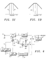
- the sample storage values S1,S2 are stored in capacitors C1 and C2, as shown in FIG. 6, by closing at the appropriate instant corresponding with switches 61,62, respectively.
- An amplifier 16 with differential inputs may be the comparator to compare the two sample storage values S1,S2, and applies a correction signal 26 to the filter tuning voltage signal 19.
- Another embodiment includes using digital techniques and/or software associated with suitable interfaces such as analogue-to-digital and digital-to-analogue converters.
- the switching action of the switches may disturb the signal at the output signal 28. Such a disturbance may be minimised by making the transition switch from F1 to F2 gradual.
- an alternating modulation signal may be added to the approximate filter tuning voltage. Any form of signal, for example a squarewave signal, a pulsed signal, a sine wave signal or a sawtooth signal may be used for the filter modulation signal to accomplish the transition from F1 to F2, however, a triangular waveform has proven to be easy to generate and does not introduce disagreeable jittering or jumping of the output signal.
- the transition and sampling periods may be synchronised with the picture field frequency.
- the sampling can take place during the vertical blanking period where disturbances to the picture will not be observed. Also, by making the transition period longer, for example by several field periods, the risk of disturbance to sound signal is reduced. As the drift of the filter with temperature is slow, for example causing a shift of several tens of kilohertz per second it is necessary, particularly in implementations using digital storage and/or software, to perform a correction cycle only periodically for example, once every second or every ten seconds. This further reduces the risk of disturbing the output signal 28.
- the sampling operation can be carried out at a time such as a programme change. It is the use of sample and hold techniques that allows the period of the filter sweep to be long, for example lasting several seconds.
- an automatic gain control may be provided with the signal processing 12.
- a variable gain controlled amplifier 32 may be placed in the signal path, either in front of or behind the filter 11.
- an error signal 34 is feedback from the output of the system with, for example level detector 13, and then applied to the variable gain amplifier 32, as shown in FIG. 4.
- the error signal 34 may be recognised as a measure of the signal level.
- the AGC may be able to minimise the amplitude modulation caused by the shifting of the filter centre frequency by the tuning modulation signal.
- the AGC circuitry for example its time constants, must be designed to minimise the amplitude modulation modulation caused by the shifting of the filter centre frequency without causing distortion of the output signal.
- An analogue TV signal consists of a picture carrier and a sound carrier.
- the power of the sound carrier is about a tenth of the picture carrier.
- the sound carrier may be for example 4.5, 5.5, 6.0 or 6.5 MHz higher in frequency than the picture carrier. If the level of the detector measures only the level of the picture carrier, the filter centre will be positioned on the picture carrier signal 42 as shown in FIG. 5a.
- a shift in the centring of the filter may be introduced into the system.
- one way to introduce a shift is by adding 53 a frequency offset 52 at the input of the comparator 16.
- the filter may be centred around an unsymmetrical signal, such as an analogue TV signal.
Landscapes
- Circuits Of Receivers In General (AREA)
- Superheterodyne Receivers (AREA)
- Networks Using Active Elements (AREA)
- Input Circuits Of Receivers And Coupling Of Receivers And Audio Equipment (AREA)
- Channel Selection Circuits, Automatic Tuning Circuits (AREA)
Abstract
Description
Claims (10)
- An apparatus (1) for tuning a filter (11) comprising:a filter (11) for receiving an input signal (10) and providing an output signal (9,28), the filter adapted to receive a tuning signal (27) to adjust the filter to provide the output signal to a desired signal, the tuning signal resulting from a modulation signal (25), a correction signal (26) andan approximate filter tuning signal (19) generated by a filter tuning signal generator (20), the modulation signal having a frequency that varies between a first frequency (F1) and a second frequency (F2), a first value (S1) of the output signal measured at the first frequency, and a second value (S2) of the output signal measured at the second frequency, a comparator (16) for comparing the first value and the second value and providing the correction signal, to adjust the filter with the tuning control signal with respect to the first frequency and the second frequency of the modulation signal, the correction signal and the approximate filter tuning signal.
- An apparatus (1) as claimed in claim 1 wherein said modulation signal (25) has a frequency that changes periodically between the first frequency (F1) and the second frequency (F2).
- An apparatus (1) as claimed in claim 1 or 2 further comprising a switch (14) to switch the frequency signals (F1,F2) that generate the first and second frequencies of the modulation signal (25).
- An apparatus (1) as claimed in any preceding claim wherein the change between the first frequency (F1) and the second frequency (F2) of the modulation signal is gradual.
- An apparatus (1) as claimed in claim 4 wherein the waveform of the alternating modulation signal (25) is triangular.
- An apparatus (1) as claimed in any preceding claim wherein the first value (S1) is stored in a first sample storage device (21) and the second value (S2) is stored in a second sample storage device (22).
- An apparatus (1) as claimed in claim 6 wherein the sample storage devices (21,22) are capacitors (C1,C2).
- An apparatus (1) as claimed in claim 6 or 7 wherein a sample switch (15) is provided for switching to the correct sample storage device (21,22).
- An apparatus (1) as claimed in claim 8 wherein the sample switch (15) and the modulation signal switch (14) are synchronised with a picture field frequency of the input signal (10).
- A method for tuning a filter:providing an input signal (10) received at a filter (11) to provide an output signal (9,28);adapting the filter to receive a tuning control signal (27), wherein the tuning control signal comprising a modulation signal alternating between a first frequency (F1) and a second frequency (F2);providing an approximate filter tuning signal (19) to the tuning control signal,measuring a first value (S1) of the output signal measured at the first frequency passing through the filter;measuring a second value (S2) of the output signal measured at the second frequency passing through the filter;comparing at a comparator the first value and the second value and providing a comparison signal to a filter tuning control signal; andadjusting the filter with the tuning control signal with respect to the first frequency and the second frequency of the modulation signal, the correction signal and the approximate filter tuning signal.
Priority Applications (4)
| Application Number | Priority Date | Filing Date | Title |
|---|---|---|---|
| AT02290380T ATE421795T1 (en) | 2002-02-18 | 2002-02-18 | DEVICE AND METHOD FOR TUNING A FILTER |
| EP02290380A EP1376853B1 (en) | 2002-02-18 | 2002-02-18 | Apparatus and method for tuning a filter |
| DE60230972T DE60230972D1 (en) | 2002-02-18 | 2002-02-18 | Apparatus and method for tuning a filter |
| US10/351,824 US6781474B2 (en) | 2002-02-18 | 2003-01-27 | Apparatus and method for tuning a filter |
Applications Claiming Priority (1)
| Application Number | Priority Date | Filing Date | Title |
|---|---|---|---|
| EP02290380A EP1376853B1 (en) | 2002-02-18 | 2002-02-18 | Apparatus and method for tuning a filter |
Publications (2)
| Publication Number | Publication Date |
|---|---|
| EP1376853A1 true EP1376853A1 (en) | 2004-01-02 |
| EP1376853B1 EP1376853B1 (en) | 2009-01-21 |
Family
ID=27675764
Family Applications (1)
| Application Number | Title | Priority Date | Filing Date |
|---|---|---|---|
| EP02290380A Expired - Lifetime EP1376853B1 (en) | 2002-02-18 | 2002-02-18 | Apparatus and method for tuning a filter |
Country Status (4)
| Country | Link |
|---|---|
| US (1) | US6781474B2 (en) |
| EP (1) | EP1376853B1 (en) |
| AT (1) | ATE421795T1 (en) |
| DE (1) | DE60230972D1 (en) |
Cited By (1)
| Publication number | Priority date | Publication date | Assignee | Title |
|---|---|---|---|---|
| US8175560B2 (en) | 2006-03-16 | 2012-05-08 | Freescale Semiconductor, Inc. | Method and system for tuning an antenna |
Families Citing this family (22)
| Publication number | Priority date | Publication date | Assignee | Title |
|---|---|---|---|---|
| US7761067B1 (en) * | 2003-05-15 | 2010-07-20 | Marvell International Ltd. | Iterative filter circuit calibration |
| US7039385B1 (en) * | 2003-06-02 | 2006-05-02 | Rockwell Collins, Inc. | Method and apparatus for automatic center frequency tuning of tunable bandpass filters |
| GB2485213B (en) * | 2010-11-05 | 2013-05-15 | Sira Consulting Ltd | Automatic termination circuit and method |
| US9899133B2 (en) | 2013-08-01 | 2018-02-20 | Qorvo Us, Inc. | Advanced 3D inductor structures with confined magnetic field |
| US9825656B2 (en) | 2013-08-01 | 2017-11-21 | Qorvo Us, Inc. | Weakly coupled tunable RF transmitter architecture |
| US9705478B2 (en) | 2013-08-01 | 2017-07-11 | Qorvo Us, Inc. | Weakly coupled tunable RF receiver architecture |
| US9484879B2 (en) | 2013-06-06 | 2016-11-01 | Qorvo Us, Inc. | Nonlinear capacitance linearization |
| US9755671B2 (en) | 2013-08-01 | 2017-09-05 | Qorvo Us, Inc. | VSWR detector for a tunable filter structure |
| US9685928B2 (en) | 2013-08-01 | 2017-06-20 | Qorvo Us, Inc. | Interference rejection RF filters |
| US9748905B2 (en) | 2013-03-15 | 2017-08-29 | Qorvo Us, Inc. | RF replicator for accurate modulated amplitude and phase measurement |
| US12224096B2 (en) | 2013-03-15 | 2025-02-11 | Qorvo Us, Inc. | Advanced 3D inductor structures with confined magnetic field |
| US9871499B2 (en) | 2013-03-15 | 2018-01-16 | Qorvo Us, Inc. | Multi-band impedance tuners using weakly-coupled LC resonators |
| US9774311B2 (en) * | 2013-03-15 | 2017-09-26 | Qorvo Us, Inc. | Filtering characteristic adjustments of weakly coupled tunable RF filters |
| US9859863B2 (en) | 2013-03-15 | 2018-01-02 | Qorvo Us, Inc. | RF filter structure for antenna diversity and beam forming |
| US9628045B2 (en) | 2013-08-01 | 2017-04-18 | Qorvo Us, Inc. | Cooperative tunable RF filters |
| US9780756B2 (en) | 2013-08-01 | 2017-10-03 | Qorvo Us, Inc. | Calibration for a tunable RF filter structure |
| US9705542B2 (en) | 2013-06-06 | 2017-07-11 | Qorvo Us, Inc. | Reconfigurable RF filter |
| US9966981B2 (en) | 2013-06-06 | 2018-05-08 | Qorvo Us, Inc. | Passive acoustic resonator based RF receiver |
| US9780817B2 (en) | 2013-06-06 | 2017-10-03 | Qorvo Us, Inc. | RX shunt switching element-based RF front-end circuit |
| US9800282B2 (en) | 2013-06-06 | 2017-10-24 | Qorvo Us, Inc. | Passive voltage-gain network |
| US10796835B2 (en) | 2015-08-24 | 2020-10-06 | Qorvo Us, Inc. | Stacked laminate inductors for high module volume utilization and performance-cost-size-processing-time tradeoff |
| US11139238B2 (en) | 2016-12-07 | 2021-10-05 | Qorvo Us, Inc. | High Q factor inductor structure |
Citations (4)
| Publication number | Priority date | Publication date | Assignee | Title |
|---|---|---|---|---|
| DE3231708A1 (en) * | 1982-08-26 | 1984-03-01 | Robert Bosch Gmbh, 7000 Stuttgart | Filter and demodulation circuit |
| US4736456A (en) | 1985-04-11 | 1988-04-05 | Deutsche Thomson-Brandt Gmbh | Tuning system for television sets |
| EP0445886A1 (en) * | 1990-03-09 | 1991-09-11 | Philips Electronique Grand Public | Television receiver with reduced threshold level frequency demodulator |
| GB2335809A (en) * | 1998-03-24 | 1999-09-29 | Ericsson Telefon Ab L M | Demodulator circuits |
Family Cites Families (4)
| Publication number | Priority date | Publication date | Assignee | Title |
|---|---|---|---|---|
| US4053933A (en) * | 1976-11-02 | 1977-10-11 | Zenith Radio Corporation | Adaptive phase locked loop filter for television tuning |
| US4272743A (en) * | 1979-04-20 | 1981-06-09 | Rca Corporation | Method for tuning a filter circuit |
| DE3510559A1 (en) * | 1985-03-21 | 1986-09-25 | H. u. C. Elektronik Hansen & Co, 1000 Berlin | CIRCUIT FOR AUTOMATIC TUNING FOR FM RECEIVERS |
| JPH03114391A (en) * | 1989-09-28 | 1991-05-15 | Toshiba Corp | Filter automatic adjustment circuit |
-
2002
- 2002-02-18 DE DE60230972T patent/DE60230972D1/en not_active Expired - Lifetime
- 2002-02-18 AT AT02290380T patent/ATE421795T1/en not_active IP Right Cessation
- 2002-02-18 EP EP02290380A patent/EP1376853B1/en not_active Expired - Lifetime
-
2003
- 2003-01-27 US US10/351,824 patent/US6781474B2/en not_active Expired - Lifetime
Patent Citations (4)
| Publication number | Priority date | Publication date | Assignee | Title |
|---|---|---|---|---|
| DE3231708A1 (en) * | 1982-08-26 | 1984-03-01 | Robert Bosch Gmbh, 7000 Stuttgart | Filter and demodulation circuit |
| US4736456A (en) | 1985-04-11 | 1988-04-05 | Deutsche Thomson-Brandt Gmbh | Tuning system for television sets |
| EP0445886A1 (en) * | 1990-03-09 | 1991-09-11 | Philips Electronique Grand Public | Television receiver with reduced threshold level frequency demodulator |
| GB2335809A (en) * | 1998-03-24 | 1999-09-29 | Ericsson Telefon Ab L M | Demodulator circuits |
Cited By (1)
| Publication number | Priority date | Publication date | Assignee | Title |
|---|---|---|---|---|
| US8175560B2 (en) | 2006-03-16 | 2012-05-08 | Freescale Semiconductor, Inc. | Method and system for tuning an antenna |
Also Published As
| Publication number | Publication date |
|---|---|
| ATE421795T1 (en) | 2009-02-15 |
| DE60230972D1 (en) | 2009-03-12 |
| EP1376853B1 (en) | 2009-01-21 |
| US6781474B2 (en) | 2004-08-24 |
| US20030155988A1 (en) | 2003-08-21 |
Similar Documents
| Publication | Publication Date | Title |
|---|---|---|
| EP1376853B1 (en) | Apparatus and method for tuning a filter | |
| US5101509A (en) | Rf filter alignment using digital processor clock | |
| FI82794B (en) | FOERFARANDE FOER AVSTAEMNING AV SVAENGNINGSKRETSARNA AV EN SIGNALMOTTAGNINGSAPPARAT. | |
| EP0618676B1 (en) | Tunable device | |
| US8340616B2 (en) | Tracking filter for tuner | |
| US7039385B1 (en) | Method and apparatus for automatic center frequency tuning of tunable bandpass filters | |
| KR20000034319A (en) | Automatic frequency tracking device of television signal receiving system and method | |
| US5991609A (en) | Low cost digital automatic alignment method and apparatus | |
| US7509106B2 (en) | Test signal generation circuit, and reception circuit | |
| US7738847B2 (en) | Automatic gain control for a tuner | |
| EP0511968A1 (en) | Interference filter for tvro receiver systems | |
| JPS60158713A (en) | Automatic regulator of communication receiver | |
| EP1156589A1 (en) | AM receiver | |
| GB2433353A (en) | YIG Filter Tuning System and Method | |
| US20090091503A1 (en) | Method and system for tuning an antenna | |
| RU2701719C1 (en) | Radio receiving device for rs with extended dynamic range | |
| CN101790059A (en) | Television tuner with high Q value tuned filter | |
| GB1565899A (en) | Circuit arrangemnt for receiving one of the sidebands of a double sideband signal | |
| KR100309097B1 (en) | Method and apparatus of fine tuning for television receiver and method and apparatus of matching vsb signal | |
| US20070002972A1 (en) | Cancellation of undesired portions of audio signals | |
| JP2000333214A (en) | Single channel spectrum analyzer | |
| KR100281361B1 (en) | Phase-locked loop FM / AM tuner with temperature compensation | |
| JPH0666704B2 (en) | Receiver | |
| KR20000031609A (en) | Apparatus for compensating weak electric field of am/fm tuners in phase locked loop | |
| JPS6174412A (en) | Television tuner |
Legal Events
| Date | Code | Title | Description |
|---|---|---|---|
| PUAI | Public reference made under article 153(3) epc to a published international application that has entered the european phase |
Free format text: ORIGINAL CODE: 0009012 |
|
| AK | Designated contracting states |
Kind code of ref document: A1 Designated state(s): AT BE CH CY DE DK ES FI FR GB GR IE IT LI LU MC NL PT SE TR |
|
| AX | Request for extension of the european patent |
Extension state: AL LT LV MK RO SI |
|
| 17P | Request for examination filed |
Effective date: 20040702 |
|
| AKX | Designation fees paid |
Designated state(s): AT BE CH CY DE DK ES FI FR GB GR IE IT LI LU MC NL PT SE TR |
|
| RAP1 | Party data changed (applicant data changed or rights of an application transferred) |
Owner name: FREESCALE SEMICONDUCTOR, INC. |
|
| 17Q | First examination report despatched |
Effective date: 20080328 |
|
| GRAP | Despatch of communication of intention to grant a patent |
Free format text: ORIGINAL CODE: EPIDOSNIGR1 |
|
| GRAS | Grant fee paid |
Free format text: ORIGINAL CODE: EPIDOSNIGR3 |
|
| GRAA | (expected) grant |
Free format text: ORIGINAL CODE: 0009210 |
|
| AK | Designated contracting states |
Kind code of ref document: B1 Designated state(s): AT BE CH CY DE DK ES FI FR GB GR IE IT LI LU MC NL PT SE TR |
|
| REG | Reference to a national code |
Ref country code: GB Ref legal event code: FG4D |
|
| REG | Reference to a national code |
Ref country code: CH Ref legal event code: EP |
|
| REG | Reference to a national code |
Ref country code: IE Ref legal event code: FG4D |
|
| REF | Corresponds to: |
Ref document number: 60230972 Country of ref document: DE Date of ref document: 20090312 Kind code of ref document: P |
|
| PG25 | Lapsed in a contracting state [announced via postgrant information from national office to epo] |
Ref country code: NL Free format text: LAPSE BECAUSE OF FAILURE TO SUBMIT A TRANSLATION OF THE DESCRIPTION OR TO PAY THE FEE WITHIN THE PRESCRIBED TIME-LIMIT Effective date: 20090121 |
|
| NLV1 | Nl: lapsed or annulled due to failure to fulfill the requirements of art. 29p and 29m of the patents act | ||
| PG25 | Lapsed in a contracting state [announced via postgrant information from national office to epo] |
Ref country code: FI Free format text: LAPSE BECAUSE OF FAILURE TO SUBMIT A TRANSLATION OF THE DESCRIPTION OR TO PAY THE FEE WITHIN THE PRESCRIBED TIME-LIMIT Effective date: 20090121 Ref country code: ES Free format text: LAPSE BECAUSE OF FAILURE TO SUBMIT A TRANSLATION OF THE DESCRIPTION OR TO PAY THE FEE WITHIN THE PRESCRIBED TIME-LIMIT Effective date: 20090502 |
|
| PG25 | Lapsed in a contracting state [announced via postgrant information from national office to epo] |
Ref country code: PT Free format text: LAPSE BECAUSE OF FAILURE TO SUBMIT A TRANSLATION OF THE DESCRIPTION OR TO PAY THE FEE WITHIN THE PRESCRIBED TIME-LIMIT Effective date: 20090622 Ref country code: SE Free format text: LAPSE BECAUSE OF FAILURE TO SUBMIT A TRANSLATION OF THE DESCRIPTION OR TO PAY THE FEE WITHIN THE PRESCRIBED TIME-LIMIT Effective date: 20090421 Ref country code: AT Free format text: LAPSE BECAUSE OF FAILURE TO SUBMIT A TRANSLATION OF THE DESCRIPTION OR TO PAY THE FEE WITHIN THE PRESCRIBED TIME-LIMIT Effective date: 20090121 |
|
| PG25 | Lapsed in a contracting state [announced via postgrant information from national office to epo] |
Ref country code: BE Free format text: LAPSE BECAUSE OF FAILURE TO SUBMIT A TRANSLATION OF THE DESCRIPTION OR TO PAY THE FEE WITHIN THE PRESCRIBED TIME-LIMIT Effective date: 20090121 Ref country code: MC Free format text: LAPSE BECAUSE OF NON-PAYMENT OF DUE FEES Effective date: 20090228 |
|
| REG | Reference to a national code |
Ref country code: CH Ref legal event code: PL |
|
| PG25 | Lapsed in a contracting state [announced via postgrant information from national office to epo] |
Ref country code: CH Free format text: LAPSE BECAUSE OF NON-PAYMENT OF DUE FEES Effective date: 20090228 Ref country code: LI Free format text: LAPSE BECAUSE OF NON-PAYMENT OF DUE FEES Effective date: 20090228 Ref country code: DK Free format text: LAPSE BECAUSE OF FAILURE TO SUBMIT A TRANSLATION OF THE DESCRIPTION OR TO PAY THE FEE WITHIN THE PRESCRIBED TIME-LIMIT Effective date: 20090121 |
|
| PLBE | No opposition filed within time limit |
Free format text: ORIGINAL CODE: 0009261 |
|
| STAA | Information on the status of an ep patent application or granted ep patent |
Free format text: STATUS: NO OPPOSITION FILED WITHIN TIME LIMIT |
|
| 26N | No opposition filed |
Effective date: 20091022 |
|
| PG25 | Lapsed in a contracting state [announced via postgrant information from national office to epo] |
Ref country code: IE Free format text: LAPSE BECAUSE OF NON-PAYMENT OF DUE FEES Effective date: 20090218 |
|
| PG25 | Lapsed in a contracting state [announced via postgrant information from national office to epo] |
Ref country code: GR Free format text: LAPSE BECAUSE OF FAILURE TO SUBMIT A TRANSLATION OF THE DESCRIPTION OR TO PAY THE FEE WITHIN THE PRESCRIBED TIME-LIMIT Effective date: 20090422 |
|
| PG25 | Lapsed in a contracting state [announced via postgrant information from national office to epo] |
Ref country code: IT Free format text: LAPSE BECAUSE OF FAILURE TO SUBMIT A TRANSLATION OF THE DESCRIPTION OR TO PAY THE FEE WITHIN THE PRESCRIBED TIME-LIMIT Effective date: 20090121 |
|
| PG25 | Lapsed in a contracting state [announced via postgrant information from national office to epo] |
Ref country code: LU Free format text: LAPSE BECAUSE OF NON-PAYMENT OF DUE FEES Effective date: 20090218 |
|
| PG25 | Lapsed in a contracting state [announced via postgrant information from national office to epo] |
Ref country code: TR Free format text: LAPSE BECAUSE OF FAILURE TO SUBMIT A TRANSLATION OF THE DESCRIPTION OR TO PAY THE FEE WITHIN THE PRESCRIBED TIME-LIMIT Effective date: 20090121 |
|
| PG25 | Lapsed in a contracting state [announced via postgrant information from national office to epo] |
Ref country code: CY Free format text: LAPSE BECAUSE OF FAILURE TO SUBMIT A TRANSLATION OF THE DESCRIPTION OR TO PAY THE FEE WITHIN THE PRESCRIBED TIME-LIMIT Effective date: 20090121 |
|
| REG | Reference to a national code |
Ref country code: GB Ref legal event code: 732E Free format text: REGISTERED BETWEEN 20120628 AND 20120704 |
|
| REG | Reference to a national code |
Ref country code: FR Ref legal event code: TP Owner name: RYO HOLDINGS, US Effective date: 20120806 |
|
| REG | Reference to a national code |
Ref country code: DE Ref legal event code: R081 Ref document number: 60230972 Country of ref document: DE Owner name: RYO HOLDINGS, LLC, US Free format text: FORMER OWNER: FREESCALE SEMICONDUCTORS, INC., AUSTIN, US Effective date: 20120905 Ref country code: DE Ref legal event code: R081 Ref document number: 60230972 Country of ref document: DE Owner name: RYO HOLDINGS, LLC, WILMINGTON, US Free format text: FORMER OWNER: FREESCALE SEMICONDUCTORS, INC., AUSTIN, TEX., US Effective date: 20120905 |
|
| REG | Reference to a national code |
Ref country code: FR Ref legal event code: PLFP Year of fee payment: 14 |
|
| PGFP | Annual fee paid to national office [announced via postgrant information from national office to epo] |
Ref country code: DE Payment date: 20150227 Year of fee payment: 14 |
|
| PGFP | Annual fee paid to national office [announced via postgrant information from national office to epo] |
Ref country code: FR Payment date: 20150126 Year of fee payment: 14 |
|
| REG | Reference to a national code |
Ref country code: DE Ref legal event code: R119 Ref document number: 60230972 Country of ref document: DE |
|
| REG | Reference to a national code |
Ref country code: FR Ref legal event code: ST Effective date: 20161028 |
|
| PG25 | Lapsed in a contracting state [announced via postgrant information from national office to epo] |
Ref country code: FR Free format text: LAPSE BECAUSE OF NON-PAYMENT OF DUE FEES Effective date: 20160229 Ref country code: DE Free format text: LAPSE BECAUSE OF NON-PAYMENT OF DUE FEES Effective date: 20160901 |
|
| PGFP | Annual fee paid to national office [announced via postgrant information from national office to epo] |
Ref country code: GB Payment date: 20180125 Year of fee payment: 17 |
|
| GBPC | Gb: european patent ceased through non-payment of renewal fee |
Effective date: 20190218 |
|
| PG25 | Lapsed in a contracting state [announced via postgrant information from national office to epo] |
Ref country code: GB Free format text: LAPSE BECAUSE OF NON-PAYMENT OF DUE FEES Effective date: 20190218 |