EP1376697A1 - Integrated-optical microsystem based on organic semiconductors - Google Patents
Integrated-optical microsystem based on organic semiconductors Download PDFInfo
- Publication number
- EP1376697A1 EP1376697A1 EP02405494A EP02405494A EP1376697A1 EP 1376697 A1 EP1376697 A1 EP 1376697A1 EP 02405494 A EP02405494 A EP 02405494A EP 02405494 A EP02405494 A EP 02405494A EP 1376697 A1 EP1376697 A1 EP 1376697A1
- Authority
- EP
- European Patent Office
- Prior art keywords
- layer
- integrated
- electrically conductive
- light
- component
- Prior art date
- Legal status (The legal status is an assumption and is not a legal conclusion. Google has not performed a legal analysis and makes no representation as to the accuracy of the status listed.)
- Withdrawn
Links
Images

Classifications
-
- H—ELECTRICITY
- H10—SEMICONDUCTOR DEVICES; ELECTRIC SOLID-STATE DEVICES NOT OTHERWISE PROVIDED FOR
- H10F—INORGANIC SEMICONDUCTOR DEVICES SENSITIVE TO INFRARED RADIATION, LIGHT, ELECTROMAGNETIC RADIATION OF SHORTER WAVELENGTH OR CORPUSCULAR RADIATION
- H10F39/00—Integrated devices, or assemblies of multiple devices, comprising at least one element covered by group H10F30/00, e.g. radiation detectors comprising photodiode arrays
- H10F39/80—Constructional details of image sensors
-
- H—ELECTRICITY
- H10—SEMICONDUCTOR DEVICES; ELECTRIC SOLID-STATE DEVICES NOT OTHERWISE PROVIDED FOR
- H10F—INORGANIC SEMICONDUCTOR DEVICES SENSITIVE TO INFRARED RADIATION, LIGHT, ELECTROMAGNETIC RADIATION OF SHORTER WAVELENGTH OR CORPUSCULAR RADIATION
- H10F39/00—Integrated devices, or assemblies of multiple devices, comprising at least one element covered by group H10F30/00, e.g. radiation detectors comprising photodiode arrays
- H10F39/80—Constructional details of image sensors
- H10F39/806—Optical elements or arrangements associated with the image sensors
- H10F39/8063—Microlenses
Definitions
- An integrated-optical microsystem comprises at least two different electronic, photonic and/or micromechanic components arranged on a common substrate.
- Important examples of such components are monochromatic (laser) or polychromatic (LED) light sources, photodetectors, photovoltaic power generators, p-channel and n-channel field-effect transistors, resistors, capacitors, light-guiding or wave-guiding structures, or derived sensing devices for the measurement of pressure, magnetic or electric fields, chemical or bio-chemical substances, etc.
- Applications include self-powered posters or business cards, millimeter-thin large-area scanners and electronic paper.
- CMOS complementary metal oxide semiconductor
- Passive optical components such as lenses, prisms or mirrors are realized with glass.
- Microoptical elements such as microlens arrays or diffractive optical components are fabricated with plastic materials, while the bodies and cases of complete systems are manufactured with metals or plastics.
- photosensitive elements, electronic devices and circuits can be combined monolithically into “smart pixels” and “smart image sensors”, preferably using silicon (cf. P. Seitz, “Smart Image Sensors: An Emerging Key Technology for Advanced Optical Measurement and Microsystems", Proc. SPIE, Vol. 2783, pp. 244-255, 1996). Due to the semiconductor properties of silicon it is difficult, however, to generate light within the same material used for the rest of the photosensitive and electronic devices.
- OEICs optoelectronic integrated circuits
- a silicon substrate contains electronic circuits, and an organic semiconducting layer is deposited on top, with which light can be emitted under control of the underlying electronic circuits.
- a hybrid solution for an optical head assembly based on an organic electroluminescent light-emitting array is described in U.S. Patent No. 6,297,842 by K. Masumi.
- the electronic circuits are contained in a silicon substrate, on top of which an organic semiconductor is deposited that generates light under control of the underlying circuits.
- These hybrid elements are then mounted on a printed circuit board to form a complete optical head assembly.
- U.S. Patent No. 5,770,446 by T. Sasaki et al. describes the monolithic combination of laser, optical amplifier, optical waveguide, optical modulator and optical switch with a suitable selection of inorganic compound semiconductors such as InP and InGaAsP.
- Devices are formed with a sequence of selective crystal growth processes using demanding metallo-organic vapor phase epitaxy, photolithographic definition of structures and suitable etching steps.
- U.S. Patent No. 6,228,670 by K. Kudo describes the monolithic combination of a highly integrated array of laser diodes, waveguides and optical amplifiers. Devices are formed with a sequence of selective crystal growth processes using demanding metallo-organic vapor phase epitaxy, photolithographic definition of structures and suitable etching steps.
- Another object is to scale up the manufacturing process to very large surfaces of square meters.
- Still another object is to significantly reduce the production costs of optical microsystems compared with the prior art.
- Yet another object is to shape the resulting microsystems in three dimensions after an essentially planar fabrication.
- Still another object is to achieve a higher degree of integration, of functionality and of system complexity than with the prior art.
- the invention discloses the monolithic integration of all key photonic components of an integrated-optical microsystem based on organic semiconductors, in particular of monochromatic (laser) or polychromatic (LED) light sources, photodetectors, photovoltaic power generators, p-channel and n-channel field-effect transistors, resistors, capacitors, light guiding or wave guiding structures, as well as derived sensing devices for the measurement of pressure, magnetic or electric fields, chemical or bio-chemical substances, etc.
- monochromatic (laser) or polychromatic (LED) light sources in particular of monochromatic (laser) or polychromatic (LED) light sources, photodetectors, photovoltaic power generators, p-channel and n-channel field-effect transistors, resistors, capacitors, light guiding or wave guiding structures, as well as derived sensing devices for the measurement of pressure, magnetic or electric fields, chemical or bio-chemical substances, etc.
- monolithic integration means in this connection that the components
- the integrated-optical microsystem comprises a substrate and a plurality of components arranged on said substrate. At least a first of said components comprises a layer of organic semiconductor material. Said first component and a second, different component are monolithically integrated on said substrate.
- said first component and said second component each comprise a plurality of layers, and said first component and said second component each comprise a corresponding layer with identical physical and chemical characteristics, and preferably with identical thicknesses and identical chemical and physical consistencies.
- said first component and said second component each comprise a plurality of corresponding layers, said corresponding layers being mutually arranged in the vertical direction in the same order.
- Said layers are, e.g., selected from the group consisting of: a first and a second electrically conductive layer, one of said electrically conductive layers being a hole injection layer and one of said electrically conductive layers being an electron injection layer; an electrical insulation layer; an organic semiconductor layer; and a light-guide or wave-guide layer.
- the method for manufacturing an integrated-optical microsystem comprises the steps of providing a substrate and arranging a plurality of components on said substrate. At least a first of said components comprises a layer of organic semiconductor material. Said first component and a second, different component are monolithically integrated on said substrate.
- the process of monolithic integration of said first component and said second component comprises the fabrication of a plurality of layers, and a corresponding layer is fabricated simultaneously in said first component and said second component.
- the process of monolithic integration of said first component and said second component comprises the fabrication of a plurality of corresponding layers in said first component and said second component, each corresponding layer being fabricated simultaneously in said first component and said second component.
- Said layers are selected, e.g., from the group consisting of a first and a second electrically conductive layer, one of said electrically conductive layers being a hole injection layer and one of said electrically conductive layers being an electron injection layer; an electrical insulation layer; an organic semiconductor layer; and a light-guide or wave-guide layer.
- terms such as “light”, “optical” or “photo" refer to any kind of electromagnetic radiation, such as visible light, infrared (IR) or ultraviolet (UV) radiation.
- FIG 1 shows a schematic cross section through an integrated-optical microsystem 1 according to the invention.
- the microsystem 1 comprises at least two different electronic, photonic and/or micromechanic components 11-16 arranged on a common substrate 20.
- the examples of such components 11-16 shown in Figure 1 are: an integrated light-emitting device 11 ( Figure 1(a) ); an integrated photodetector or photovoltaic cell 12 ( Figure 1(b) ); an integrated n-channel field-effect transistor (FET) 13 ( Figure 1(c) ); an integrated p-channel FET 14 ( Figure 1(d) ); an integrated capacitor 15 ( Figure 1(e) ); and/or an interconnect region 16 between two conductive layers (hole and electron injectors) ( Figure 1(f) ).
- an integrated light-emitting device 11 Figure 1(a)
- an integrated photodetector or photovoltaic cell 12 Figure 1(b)
- FET field-effect transistor
- Figure 1(d) an integrated p-channel FET 14
- the substrate 20 may be transparent or opaque, and may be rigid or flexible, depending on the envisaged application.
- Examples of structures usable as substrates 20 are the well-known silicon wafer, thin stainless steel foils, or transparent plastics such as polyester (PET, Mylar®), polyimide (Kapton®), polyamides (Nylon®), polypropylene or polyethylene.
- the components 11-16 arranged on the common substrate 20 are compatible with each other, can be manufactured simultaneously and can be operated simultaneously. They are built up from a set of elements, typically structured layers 21-26 of various materials, examples of which are given in the following with reference to Figure 1.
- Reference sign 21 denotes a hole injection layer that is transparent or opaque.
- Reference signs 22 and 24 denote a first and second insulation layer, respectively.
- Reference sign 23 denotes an active organic semiconductor layer.
- Reference sign 25 denotes an injection layer that is transparent or opaque.
- Reference sign 26 denotes a light-guiding or wave-guiding layer.
- a component does not necessarily contain all of the set of elements 21-26, and the elements 21-26 may be differently structured in different components 11-16.
- the corresponding layers 21-26 in each component 11-16 have the same thickness, the same chemical and physical consistency and are mutually arranged in the vertical direction z in the same order.
- a wave-guide structure can be employed, requiring a matched layer thickness of 100 to 2000 nm.
- a light-guiding structure with a thickness of 1 micrometer up to several millimeters is more appropriate.
- Preferred materials for the waveguide or light guide 26 are polymers such as PMMA (poly methyle acrylate), PC (poly carbonate), polyimide or PVC (poly vinyl chloride), or Sol-Gelmaterials such as Ormocer®.
- the geometrical definition of these waveguiding or light-guiding structures preferably occurs with a replication process such as hot embossing, UV casting, rubber stamping or injection molding.
- Organic semiconductors 23 can also be selectively deposited in thin layers by alternate, inexpensive techniques such as ink jet printing, screen printing, rubber-stamping or micro-molding (cf. H. Sirringhaus, T. Kawase and R. H. Friend, "Emerging Methods for Micro- and Nanofabrication - High-Resolution InkJet Printing of All-Polymer Transistor Circuits", MRS Bulletin - Materials Research Society, Vol. 26, pp. 539 - 543, 2001).
- the manufacturing method described above is only a preferred, simple example. A person skilled in the art having knowledge of the invention will be able to derive further processes for manufacturing a microsystem 1 according to the invention.
- the common characteristics of these manufacturing methods is the capability of developing controlled thicknesses of material (several 10 nm up to a few micrometers) in controlled geometrical patterns (spatial resolution of some 10 nm to several 10 micrometers).
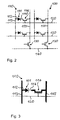
- one terminal 112 of a light-emitting-diode (LED) structure 111 is connected to a fixed-voltage line 113, while the other terminal 114 is connected via a transistor switch 116 to a variable-voltage line 115, as schematically illustrated in Figure 2 .
- a two-dimensional array 100 of one or more of such LED/transistor unit cells 110 is provided with at least one row-select line 120 that is connected to all gates of the transistor switches 116 in a row.
- the transistor switches 116 of each row have their drain contacts connected to a column line 115.
- Each column line 115 is connected via a column-select transistor 130 to a common signal line 140.
- Figure 3 shows a preferred realization of an active-pixel-LED-display unit cell 110, making use of the fabrication process explained with reference to Fig. 1.
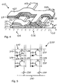
- a preferred implementation of the same active-pixel-LED-display unit cell 110 is shown in a perspective view in Figure 4 .
- identical reference signs are used for elements already introduced with reference to Figures 1 and 2.
- An individual LED 111 is lighted by connecting it to the signal line 140. This is accomplished by applying the correct potential to the row-select lines 120: in the case of p-channel transistors, a negative potential must be applied, in the case of n-channel transistors, a positive potential must be applied to render the switch transistors 116 conductive.
- the column line 115 of the LED 111 that needs to be lighted is connected via the appropriate column-select transistor 130 to the common signal line, by applying a suitable potential to the gate of this column-select transistor 130, in the same way as for the row-select transistors 116. In this way, an electrically conductive path is created from the fixed-voltage line 113 to the signal line 140 through the LED 111 that needs to be lighted.
- the intensity of the LED is controlled by the amount of current that flows through it, and this can be controlled with the signal line. If the total resistance of the current path is well known in advance (if the fabrication process is well controlled), then it is sufficient to apply a suitable potential to the signal line to achieve a predictable brightness of the LED. Otherwise, an electronic circuit is required. in the signal that sources the required amount of current (so-called current-source circuit).
- the two-dimensional array 100 of active-pixel LEDs 110 consists of a large number of LEDs, then an individual LED 111 is only switched on for a comparatively short time. This leads to a lower overall brightness of the created image.
- This limitation can be overcome with the circuit 200 shown in Figure 5 , making it possible to illuminate all LEDs 211 with their appropriate brightness at the same time. This is achieved by supplying each LED 211 with a current-source transistor 217, where the current-source transistors 217 of all pixels 210 are tied to the same potential, preferably to ground on a ground line 218.
- each current-source transistor 217 can be programmed to a specific voltage with the row-selection mechanism 216, 220, column-selection mechanism 230, 215 and signal-line voltage mechanism 240 described above with reference to Figures 2-4.
- an additional capacitance 219 can be added at the gate of the current-source transistor 217 in each pixel 210.
- the other terminal of the LED 211 is connected to a fixed-voltage line 213, in analogy to Figures 2-4.
- Excellent image sensors based on photodiodes can be realized with the active-pixel-sensor (APS) architecture for silicon-based photosensors.
- APS active-pixel-sensor
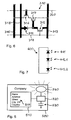
- Such an APS pixel 310 and an image sensor based on it can be realized with the process according to the invention, as illustrated in Figure 6 .
- a photodiode 311 is reverse-biased to a reference voltage on a reference-voltage line 313 with a reset transistor 312, the gate of which is connected to a reset line 314.
- the other terminal of the photodiode 311 is connected to a ground line 318.
- the incident light partly discharges the photodiode 311 to a voltage value that can be measured with a source follower comprising a source-follower transistor 317 and a load resistor that is common to all APS pixels 310 at the end of a common signal line 315.
- the individual pixels 310 are connected to the common signal line 315 with a pass transistor 316, whose gate is connected row-wise to a row-selection line 320. Addressing occurs similarly to the active-pixel LEDs 210 described above with reference to Figures 2-5.
- a very simple self-powered display 400 is shown in Figure 7 . It consists of one or a series connection of one or more photoemissive elements 411 and photovoltaic elements 412.1, 412.2.
- FIG. 8 A preferred realization of an integrated self-powered display 500 is illustrated in Figure 8 . It comprises one or several photovoltaic elements or cells 510 that are either connected in parallel or in series. A series connection allows for the simple generation of higher voltages.
- the photovoltaic cells 510 can be realized as simple rectangular shapes, or they can be realized in complex forms such as letters, digits or images. It is possible to print information 511 on the photovoltaic elements 510, as long as there is sufficient free space for the photovoltaic generation of the required electric power.
- the photovoltaic elements 510 are connected to an electronic circuit 520 that carries out one or more of the following functions: voltage conversion, voltage regulation, current limitation, power management, clock generation, flashing effects, etc.
- the electronics 520 can be connected to an integrated capacitive device 530 for temporary power filtering and storage (during periods of insufficient illumination of the photovoltaic element).
- the electronics 520 feeds power to one or more photoemissive surfaces 540 that can be arbitrarily shaped. It is possible to print opaque structures on the photoemissive surfaces 540.
- the electronics 520 can drive the photoemissive structures 540 either continuously or temporally intermittently for effects such as flashing, running lights or simulated movement. It is also possible to integrate a display 100, 200 as described above with reference to Figures 2 or 5, on which moving images can be shown.
- the integrated-optical microsystems according to the invention are especially useful for the realization of many types of optical measurement principles, because the microsystem can be bent into a large variety of three-dimensional shapes after planar fabrication, provided a flexible substrate is used.
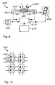
- a power-supply unit 610 provides electric power, either by drawing it from a storage device such as a battery or a charged capacitor, or by producing it with an integrated photovoltaic device comprising a series connection of one or more photodiodes under illumination that are used as photovoltaic elements (cf. Fig. 7, reference signs 412.1, 412.2).
- This electric power is managed and distributed by an electronic control circuit 620 for controlling the device 600, converting voltages, limiting electrical current, acquiring and processing signals, managing power, controlling the display of results, etc.
- the circuit 620 powers one or more light-emitting devices 640 (LEDs, superluminescent diodes, laser diodes, etc.).
- emitted light 641 can already be modulated by the driving circuit 620, for example by carrying out a temporal amplitude modulation.
- the emitted light 641 is guided with a suitable light guide or waveguide 650 near the surface of the integrated-optical microsystem 600 to a region of interaction 660.
- the light 641 interacts with the objects 661 under study according to the effects described in R. E. Kunz's paper, e.g., it is influenced by the measurand 661 in intensity, polarization, wavelength etc.
- the light 642 that is guided further carries now information in the form of changed position, modified intensity, modified polarization, modified wavelength, modified contrast, altered temporal modulation properties, etc.
- At the end of the light guide or waveguide 650 are arranged one or more photodetectors 670 that detect the light 642 carrying the desired information.
- a suitable type of detection principle must be chosen, as described in the literature.
- the measurement results are processed and interpreted by the electronic circuit 620, producing a measurement result that is either displayed locally or that is transmitted outside the optical microsystem 600 with a suitable interface 680, using electrical, optical or other transmission principles.
- the interface may, e.g., have electrical contacts or an optical interface device comprising at least one photoemissive and one photodetecting element.
- a display 690 of the microsystem 600 can be realized as one or more indicator LEDs of the same or of different color, as numeric (seven-segment) display, as alphanumeric display or as a display with full graphic capability according to Figs. 2 or 5.
- the co-integration of one or several of these various types of displays with the optical microsystem 600 is possible with the fabrication process according to the invention and illustrated with reference to Fig. 1.
- An optoelectronic scanner that is as thin as a sheet of paper can be realized with the components described above, according to the invention. It comprises a two-dimensional array 700 of one or more unit cells 710, each realized as a combination of one or more active-pixel light-emission cells 110 (or 210) such as discussed with reference to Fig. 2 (or 5, respectively), and one or more APS light sensing cells 310 such as discussed with reference to Fig. 6.
- the array 700 is schematically illustrated in Figure 10 .
- Each active-pixel LED 110 and each APS sensor pixel 310 can be addressed individually, making use of appropriate row-selection and column-selection mechanisms described above.
- the scanning process consists of resetting first the APS pixel 310, then switching on the pixel LED 110 for illumination of the local environment for a certain time, and finally reading out the APS pixel 310. If a reflecting (bright) object was lying next to the scanner cell 710, then a high reflection value will be read; if the object was locally dark (in printed areas), a lower reflection value will be read.
- the two-dimensional pattern of reflection values represent an image of the object (e.g., a document) close to the surface of the scanner cells 710.
- microlenses or gradient-index (GRIN) lenses can be placed over the scanner unit cells 710, as is known from facsimile scanning machines.
- the LEDs 110 are lighted sequentially (one at a time), larger numbers such as complete lines or extended areas are lighted at a time, or all LEDs 110 are lighted simultaneously.
- the sheet scanner 700 described above and illustrated in Figure 10 can also be used as electronic paper which, together with an appropriate pen, is part of an electronic writing equipment.
- the pen for writing on the paper can either be active or passive.
- a passive pen has a well-reflecting tip, realized for example with retroreflecting microprisms or microspheres, or with a metallic or white coating.
- the sheet scanner is operated as for the scanning purpose described above. At the position of the writing pen's tip a high reflection value will be read. The corresponding pixel LED 110 will be illuminated and stays illuminated, showing the locations where the pen has been.
- the scanning operation with a passive pen consumes a significant amount of electrical power because each position measurement requires the illumination of a large number of pixel LEDs.
- the active pen has a small area at the tip with a diameter of, e.g., 5 mm or less, from which light is emitted. This light is generated in the pen, for example with an LED.
- the scanning operation comprises the steps of resetting the APS sensing pixels 310 and reading out the values after a short exposure time of, e.g., less than 100 ms. In locations where the pen's tip has emitted enough light to create an appreciable signal in the APS pixels 310, the pixel LEDs 110 are switched on continuously, to indicate where the pen has been.
- a monolithic pocket calculator, data entry and data display system can be realized with the components described above, according to the invention.
- the keys are realized as scanner unit cells 710, as described above. When a finger comes close to the surface, the local reflection increases, and it can be detected that "the key has been pressed".
- the display unit can either consist of traditional seven-segment numeric LEDs or a fine-grained rectangular array of LEDs for higher-resolved display of numerals, characters and images.
- An integrated electronic circuit provides the power management, the key reading functions, drives the display, carries out all necessary calculations and provides for electrical, optical or other interfaces, as described above.
Landscapes
- Light Receiving Elements (AREA)
Abstract
Description
- are arranged on a common substrate,
- are compatible with each other,
- can be manufactured simultaneously and
- can be operated simultaneously.
- Since the fabrication process is monolithic, the complete optical microsystem can be fabricated with it, avoiding any cost for assembly and further hybrid system integration.
- The fabrication process can be scaled up to very large surfaces of square meters, and all technological steps to perform this are within the state of the art. This allows the fabrication of large-area optical microsystems or the simultaneous fabrication of a very large number of smaller optical microsystems.
- Because of the economy of scale and the obsolete additional assembly steps, production costs of optical microsystems fabricated according to this invention can be significantly lowered.
- The resulting microsystems can be arbitrarily shaped in three dimensions after essentially planar fabrication, provided a flexible substrate is used.
- The large number and diversity of photonic devices that can be monolithically integrated allows a higher degree of integration, of functionality and of system complexity than was practical with the state of the art.
- Figure 1
- shows a schematic cross sections through an integrated-optical microsystem according to the invention, with various integrated-optical components.
- Figure 2
- shows a schematic circuit diagram of a first embodiment of a display according to the invention.
- Figure 3
- schematically shows a pixel of an active display according to the invention.
- Figure 4
- shows a schematic perspective view of a preferred implementation of the active pixel of Fig. 8.
- Figure 5
- shows a schematic circuit diagram of a second embodiment of a display according to the invention.
- Figure 6
- schematically shows a preferred embodiment of an active pixel of a detector according to the invention.
- Figure 7
- shows a circuit diagram of a simple self powered display according to the invention.
- Figure 8
- schematically illustrates an integrated, self-powered display according to the invention.
- Figure 9
- shows a schematic diagram of an integrated-optical microsystem according to the invention.
- Figure 10
- schematically illustrates a monolithic sheet scanner of electronic paper according to the invention.
- 1
- Microsystem
- 11
- Integrated light-emitting device
- 12
- Integrated photodetector or photovoltaic cell
- 13
- Integrated n-channel FET
- 14
- Integrated p-channel FET
- 15
- Integrated capacitor
- 16
- Interconnect region
- 20
- Substrate
- 21
- Hole injection layer
- 22
- First insulation layer
- 23
- Active organic semiconductor layer
- 24
- Second insulation layer
- 25
- Injection layer
- 26
- Light-guiding or wave-guiding layer
- 100
- Active-pixel display
- 110
- Active-pixel-display unit cell
- 111
- LED structure
- 112, 114
- Terminals of LED structure
- 113
- Fixed-voltage line
- 115
- Variable-voltage line
- 116
- Row-select transistor
- 120
- Row-select line
- 130
- Column-select transistor
- 140
- Common signal line
- 200
- Active-pixel display
- 210
- Active-pixel-display unit cell
- 211
- LED structure
- 213
- Fixed-voltage line
- 215
- Variable-voltage line
- 216
- Row-select transistor
- 217
- Current-source transistor
- 218
- Ground line
- 219
- Capacitance
- 220
- Row-select line
- 230
- Column-select transistor
- 240
- Common signal line
- 310
- APS pixel
- 311
- Photodiode
- 312
- Reset transistor
- 313
- Reference-voltage line
- 314
- Reset line
- 315
- Common signal line
- 316
- Pass transistor
- 317
- Source-follower transistor
- 318
- Ground line
- 320
- Row-select line
- 400
- Self-powered display
- 411
- Photoemissive element
- 412
- Photovoltaic element
- 500
- Self-powered display
- 510
- Photovoltaic element
- 511
- Information on photovoltaic element
- 520
- Electronic circuit
- 530
- Integrated capacitive device
- 540
- Photoemissive surface
- 600
- Integrated-optical microsystem
- 610
- Power-supply unit
- 620
- Electronic control circuit
- 640
- Light-emitting device
- 641
- Emitted light
- 642
- Guided light carrying information
- 650
- Light guide or waveguide
- 660
- Region of interaction
- 661
- Measurand
- 670
- Photodetector
- 680
- Interface
- 690
- Display
- 700
- Sheet scanner
- 710
- Unit cell
Claims (26)
characterized in that
said first component (11) and a second, different component (12-16) are monolithically integrated on said substrate (20).
said light-emitting diode structure (111, 211) and said switch transistor (116, 216) are components of an integrated-optical microsystem (1) according to any of the claims 1-12.
said source-follower transistor (317), said reset transistor (312) and said photodiode (311) are components of an integrated-optical microsystem (1) according to any of the claims 1-12.
said light-emitting unit comprises an active-pixel light-emitting diode display cell (110, 210) according to claim 13 and
said light-detecting unit comprises an active-pixel photosensor or image sensor cell (310) according to claim 14.
said pen has a reflecting or light-emitting tip and
said paper is an electronic paper comprising a sheet scanner according to claim 15.
said key unit comprises a sheet scanner according to claim 15.
said photoemissive element (411, 540) and said photovoltaic element (412.1, 412.2, 510) are components of an integrated-optical microsystem (1) according to any of the claims 1-12.
said light-emitting device (640), said light guide or waveguide (650) and said photodetector (670) are components of an integrated-optical microsystem (1) according to any of the claims 1-12.
at least a first (11) of said components (11-16) comprising a layer (23) of organic semiconductor material,
said first component (11) and a second, different component (12-16) are monolithically integrated on said substrate (20).
an organic semiconductor layer (23), and
a light-guide or wave-guide layer (26).
Priority Applications (2)
| Application Number | Priority Date | Filing Date | Title |
|---|---|---|---|
| EP02405494A EP1376697A1 (en) | 2002-06-17 | 2002-06-17 | Integrated-optical microsystem based on organic semiconductors |
| US10/462,439 US7038235B2 (en) | 2002-06-17 | 2003-06-16 | Integrated-optical microsystem based on organic semiconductors |
Applications Claiming Priority (1)
| Application Number | Priority Date | Filing Date | Title |
|---|---|---|---|
| EP02405494A EP1376697A1 (en) | 2002-06-17 | 2002-06-17 | Integrated-optical microsystem based on organic semiconductors |
Publications (1)
| Publication Number | Publication Date |
|---|---|
| EP1376697A1 true EP1376697A1 (en) | 2004-01-02 |
Family
ID=29716986
Family Applications (1)
| Application Number | Title | Priority Date | Filing Date |
|---|---|---|---|
| EP02405494A Withdrawn EP1376697A1 (en) | 2002-06-17 | 2002-06-17 | Integrated-optical microsystem based on organic semiconductors |
Country Status (2)
| Country | Link |
|---|---|
| US (1) | US7038235B2 (en) |
| EP (1) | EP1376697A1 (en) |
Cited By (3)
| Publication number | Priority date | Publication date | Assignee | Title |
|---|---|---|---|---|
| DE102004059233A1 (en) * | 2004-12-08 | 2006-06-14 | Infineon Technologies Ag | Production of an optical structure comprises encasing a semiconductor component with an optically transparent material which is opaque to a high energy beam and irradiating each region of the sleeve produced with high energy radiation |
| DE102005055278A1 (en) * | 2005-11-17 | 2007-05-31 | Siemens Ag | Organic pixelated flat detector with increased sensitivity |
| US7974508B2 (en) | 2009-02-03 | 2011-07-05 | Nitto Denko Corporation | Multi-layer structure and method for manufacturing the same |
Families Citing this family (22)
| Publication number | Priority date | Publication date | Assignee | Title |
|---|---|---|---|---|
| WO2004025747A2 (en) * | 2002-09-05 | 2004-03-25 | Konarka Technologies, Inc. | Organic photovoltaic component and method for production thereof |
| US20060000542A1 (en) * | 2004-06-30 | 2006-01-05 | Yongki Min | Metal oxide ceramic thin film on base metal electrode |
| WO2006010615A1 (en) * | 2004-07-28 | 2006-02-02 | Quantum Semiconductor Llc | Layouts for the monolithic integration of cmos and deposited photonic active layers |
| US7290315B2 (en) * | 2004-10-21 | 2007-11-06 | Intel Corporation | Method for making a passive device structure |
| US20060099803A1 (en) * | 2004-10-26 | 2006-05-11 | Yongki Min | Thin film capacitor |
| US20060091495A1 (en) * | 2004-10-29 | 2006-05-04 | Palanduz Cengiz A | Ceramic thin film on base metal electrode |
| US8063473B1 (en) * | 2004-11-29 | 2011-11-22 | The United States Of America As Represented By The Secretary Of The Navy | Nanophotonic transceiver |
| US7629269B2 (en) * | 2005-03-31 | 2009-12-08 | Intel Corporation | High-k thin film grain size control |
| US20060220177A1 (en) * | 2005-03-31 | 2006-10-05 | Palanduz Cengiz A | Reduced porosity high-k thin film mixed grains for thin film capacitor applications |
| US7375412B1 (en) * | 2005-03-31 | 2008-05-20 | Intel Corporation | iTFC with optimized C(T) |
| US7453144B2 (en) * | 2005-06-29 | 2008-11-18 | Intel Corporation | Thin film capacitors and methods of making the same |
| EP1905099A4 (en) * | 2005-07-15 | 2017-07-19 | Merck Patent GmbH | Diffraction foils |
| GB2432722A (en) * | 2005-11-25 | 2007-05-30 | Seiko Epson Corp | Electrochemical cell and method of manufacture |
| GB2432723B (en) * | 2005-11-25 | 2010-12-08 | Seiko Epson Corp | Electrochemical cell and method of manufacture |
| GB2432721B (en) * | 2005-11-25 | 2011-06-22 | Seiko Epson Corp | Electrochemical cell structure and method of fabrication |
| US9217868B2 (en) | 2007-01-12 | 2015-12-22 | Kopin Corporation | Monocular display device |
| CN101632033B (en) * | 2007-01-12 | 2013-07-31 | 寇平公司 | Head-mounted monocular display device |
| US7916984B2 (en) * | 2007-03-16 | 2011-03-29 | Electronics And Telecommunications Research Institute | Opto-electric bus module and method of manufacturing the same |
| TWI355106B (en) * | 2007-05-07 | 2011-12-21 | Chunghwa Picture Tubes Ltd | Organic photodetector and fabricating method of or |
| US20100196588A1 (en) * | 2009-02-03 | 2010-08-05 | Nitto Denko Corporation | Method of manufacturing a multi-layer structure |
| US20100195952A1 (en) * | 2009-02-03 | 2010-08-05 | Nitto Denko Corporation | Multi-layer structure |
| CN113433617B (en) * | 2021-05-24 | 2022-12-20 | 金华博蓝特新材料有限公司 | Planar optical waveguide and its preparation method |
Citations (6)
| Publication number | Priority date | Publication date | Assignee | Title |
|---|---|---|---|---|
| EP0653741A1 (en) * | 1993-10-12 | 1995-05-17 | Nec Corporation | Current-controlled luminous element array and method for producing the same |
| GB2315594A (en) * | 1996-07-22 | 1998-02-04 | Cambridge Display Tech Ltd | Sensing device comprising coplanar light emitter and detectors |
| WO1999054936A1 (en) * | 1998-04-16 | 1999-10-28 | Cambridge Display Technology Ltd. | Polymer devices |
| EP0962984A2 (en) * | 1998-05-29 | 1999-12-08 | Lucent Technologies Inc. | Thin-film transistor monolithically integrated with an organic light-emitting diode |
| EP1033765A2 (en) * | 1999-03-03 | 2000-09-06 | Pioneer Corporation | Switching element and electroluminescence element display device |
| EP1164641A2 (en) * | 2000-06-12 | 2001-12-19 | Semiconductor Energy Laboratory Co., Ltd. | Light emitting module and method of driving the same, and optical sensor |
Family Cites Families (2)
| Publication number | Priority date | Publication date | Assignee | Title |
|---|---|---|---|---|
| SE470147B (en) * | 1992-04-16 | 1993-11-15 | Ericsson Telefon Ab L M | Enclosure for optical waveguide |
| US5907160A (en) * | 1996-12-20 | 1999-05-25 | Xerox Corporation | Thin film organic light emitting diode with edge emitter waveguide |
-
2002
- 2002-06-17 EP EP02405494A patent/EP1376697A1/en not_active Withdrawn
-
2003
- 2003-06-16 US US10/462,439 patent/US7038235B2/en not_active Expired - Fee Related
Patent Citations (6)
| Publication number | Priority date | Publication date | Assignee | Title |
|---|---|---|---|---|
| EP0653741A1 (en) * | 1993-10-12 | 1995-05-17 | Nec Corporation | Current-controlled luminous element array and method for producing the same |
| GB2315594A (en) * | 1996-07-22 | 1998-02-04 | Cambridge Display Tech Ltd | Sensing device comprising coplanar light emitter and detectors |
| WO1999054936A1 (en) * | 1998-04-16 | 1999-10-28 | Cambridge Display Technology Ltd. | Polymer devices |
| EP0962984A2 (en) * | 1998-05-29 | 1999-12-08 | Lucent Technologies Inc. | Thin-film transistor monolithically integrated with an organic light-emitting diode |
| EP1033765A2 (en) * | 1999-03-03 | 2000-09-06 | Pioneer Corporation | Switching element and electroluminescence element display device |
| EP1164641A2 (en) * | 2000-06-12 | 2001-12-19 | Semiconductor Energy Laboratory Co., Ltd. | Light emitting module and method of driving the same, and optical sensor |
Cited By (5)
| Publication number | Priority date | Publication date | Assignee | Title |
|---|---|---|---|---|
| DE102004059233A1 (en) * | 2004-12-08 | 2006-06-14 | Infineon Technologies Ag | Production of an optical structure comprises encasing a semiconductor component with an optically transparent material which is opaque to a high energy beam and irradiating each region of the sleeve produced with high energy radiation |
| DE102005055278A1 (en) * | 2005-11-17 | 2007-05-31 | Siemens Ag | Organic pixelated flat detector with increased sensitivity |
| DE102005055278B4 (en) * | 2005-11-17 | 2010-12-02 | Siemens Ag | Organic pixelated flat detector with increased sensitivity |
| US7875841B2 (en) | 2005-11-17 | 2011-01-25 | Siemens Aktiengesellschaft | Organic pixeled flat detector having increased sensitivity |
| US7974508B2 (en) | 2009-02-03 | 2011-07-05 | Nitto Denko Corporation | Multi-layer structure and method for manufacturing the same |
Also Published As
| Publication number | Publication date |
|---|---|
| US20030230768A1 (en) | 2003-12-18 |
| US7038235B2 (en) | 2006-05-02 |
Similar Documents
| Publication | Publication Date | Title |
|---|---|---|
| US7038235B2 (en) | Integrated-optical microsystem based on organic semiconductors | |
| US11037012B2 (en) | Image acquisition system | |
| US7601942B2 (en) | Optoelectronic device having an array of smart pixels | |
| US9632344B2 (en) | Use of LED or OLED array to implement integrated combinations of touch screen tactile, touch gesture sensor, color image display, hand-image gesture sensor, document scanner, secure optical data exchange, and fingerprint processing capabilities | |
| US7745817B2 (en) | Combined information display and information input device | |
| US9626023B2 (en) | LED/OLED array approach to integrated display, lensless-camera, and touch-screen user interface devices and associated processors | |
| US8399821B2 (en) | Light source integrated photoelectric conversion apparatus | |
| WO2018218936A1 (en) | Pixel circuit, driving method therefor, and display panel | |
| US10546970B2 (en) | Color imaging using array of wavelength-selective optoelectronic elements as light-field or image sensor and additionally capable of emitting light | |
| KR20010040510A (en) | Organic Diodes with Switchable Photosensitivity | |
| KR102667945B1 (en) | Display Device | |
| US20070057793A1 (en) | Contact array RFID readable input substrates and processes | |
| WO2018171174A1 (en) | Display panel and display apparatus | |
| KR20050001389A (en) | Display apparatus | |
| US11749659B2 (en) | Input sensing device and a display device including the same | |
| CN114342082A (en) | Detection device | |
| EP2073287B1 (en) | Layered Structures | |
| US20030121976A1 (en) | Organic light sensors for use in a mobile communication device | |
| US20050247978A1 (en) | Solution-processed thin film transistor | |
| WO2012164259A1 (en) | Electronic devices | |
| US12272302B2 (en) | Display, display fabrication method, and electronic device | |
| KR20230024851A (en) | Sensing device and electronic device | |
| TW202301720A (en) | Electronic apparatus and electronic apparatus authentication method | |
| KR20230143675A (en) | Display device and driving method of the same | |
| B&diaeru et al. | Integrated optical proximity sensor based on organic photodiodes and organic LEDs |
Legal Events
| Date | Code | Title | Description |
|---|---|---|---|
| PUAI | Public reference made under article 153(3) epc to a published international application that has entered the european phase |
Free format text: ORIGINAL CODE: 0009012 |
|
| AK | Designated contracting states |
Kind code of ref document: A1 Designated state(s): AT BE CH CY DE DK ES FI FR GB GR IE IT LI LU MC NL PT SE TR |
|
| AX | Request for extension of the european patent |
Extension state: AL LT LV MK RO SI |
|
| 17P | Request for examination filed |
Effective date: 20040223 |
|
| AKX | Designation fees paid |
Designated state(s): CH DE FR GB LI |
|
| 17Q | First examination report despatched |
Effective date: 20071018 |
|
| RAP1 | Party data changed (applicant data changed or rights of an application transferred) |
Owner name: CSEM CENTRE SUISSE D'ELECTRONIQUE ET DE MICROTECHN |
|
| STAA | Information on the status of an ep patent application or granted ep patent |
Free format text: STATUS: EXAMINATION IS IN PROGRESS |
|
| STAA | Information on the status of an ep patent application or granted ep patent |
Free format text: STATUS: THE APPLICATION IS DEEMED TO BE WITHDRAWN |
|
| 18D | Application deemed to be withdrawn |
Effective date: 20180124 |
|
| RIC1 | Information provided on ipc code assigned before grant |
Ipc: H01L 27/00 20060101AFI20030306BHEP |