EP1376527A2 - Image display - Google Patents
Image display Download PDFInfo
- Publication number
- EP1376527A2 EP1376527A2 EP03252591A EP03252591A EP1376527A2 EP 1376527 A2 EP1376527 A2 EP 1376527A2 EP 03252591 A EP03252591 A EP 03252591A EP 03252591 A EP03252591 A EP 03252591A EP 1376527 A2 EP1376527 A2 EP 1376527A2
- Authority
- EP
- European Patent Office
- Prior art keywords
- light
- coupled
- raster
- display
- cell
- Prior art date
- Legal status (The legal status is an assumption and is not a legal conclusion. Google has not performed a legal analysis and makes no representation as to the accuracy of the status listed.)
- Withdrawn
Links
- 238000000034 method Methods 0.000 claims abstract description 27
- 238000004146 energy storage Methods 0.000 claims description 8
- 238000007599 discharging Methods 0.000 claims 2
- 230000003213 activating effect Effects 0.000 claims 1
- 230000008569 process Effects 0.000 description 20
- 230000007704 transition Effects 0.000 description 16
- 239000003990 capacitor Substances 0.000 description 14
- 238000010586 diagram Methods 0.000 description 10
- 230000004913 activation Effects 0.000 description 9
- 230000008859 change Effects 0.000 description 8
- 230000003292 diminished effect Effects 0.000 description 8
- 230000008901 benefit Effects 0.000 description 4
- 230000003068 static effect Effects 0.000 description 4
- 239000004020 conductor Substances 0.000 description 3
- 230000006870 function Effects 0.000 description 3
- 230000004048 modification Effects 0.000 description 3
- 238000012986 modification Methods 0.000 description 3
- 238000006467 substitution reaction Methods 0.000 description 3
- 230000005669 field effect Effects 0.000 description 2
- 239000011159 matrix material Substances 0.000 description 2
- 239000004973 liquid crystal related substance Substances 0.000 description 1
- 230000009467 reduction Effects 0.000 description 1
- 230000000630 rising effect Effects 0.000 description 1
- 239000010409 thin film Substances 0.000 description 1
Images


Classifications
-
- G—PHYSICS
- G09—EDUCATION; CRYPTOGRAPHY; DISPLAY; ADVERTISING; SEALS
- G09G—ARRANGEMENTS OR CIRCUITS FOR CONTROL OF INDICATING DEVICES USING STATIC MEANS TO PRESENT VARIABLE INFORMATION
- G09G3/00—Control arrangements or circuits, of interest only in connection with visual indicators other than cathode-ray tubes
- G09G3/02—Control arrangements or circuits, of interest only in connection with visual indicators other than cathode-ray tubes by tracing or scanning a light beam on a screen
-
- G—PHYSICS
- G09—EDUCATION; CRYPTOGRAPHY; DISPLAY; ADVERTISING; SEALS
- G09G—ARRANGEMENTS OR CIRCUITS FOR CONTROL OF INDICATING DEVICES USING STATIC MEANS TO PRESENT VARIABLE INFORMATION
- G09G3/00—Control arrangements or circuits, of interest only in connection with visual indicators other than cathode-ray tubes
- G09G3/20—Control arrangements or circuits, of interest only in connection with visual indicators other than cathode-ray tubes for presentation of an assembly of a number of characters, e.g. a page, by composing the assembly by combination of individual elements arranged in a matrix no fixed position being assigned to or needed to be assigned to the individual characters or partial characters
- G09G3/22—Control arrangements or circuits, of interest only in connection with visual indicators other than cathode-ray tubes for presentation of an assembly of a number of characters, e.g. a page, by composing the assembly by combination of individual elements arranged in a matrix no fixed position being assigned to or needed to be assigned to the individual characters or partial characters using controlled light sources
- G09G3/30—Control arrangements or circuits, of interest only in connection with visual indicators other than cathode-ray tubes for presentation of an assembly of a number of characters, e.g. a page, by composing the assembly by combination of individual elements arranged in a matrix no fixed position being assigned to or needed to be assigned to the individual characters or partial characters using controlled light sources using electroluminescent panels
- G09G3/32—Control arrangements or circuits, of interest only in connection with visual indicators other than cathode-ray tubes for presentation of an assembly of a number of characters, e.g. a page, by composing the assembly by combination of individual elements arranged in a matrix no fixed position being assigned to or needed to be assigned to the individual characters or partial characters using controlled light sources using electroluminescent panels semiconductive, e.g. using light-emitting diodes [LED]
-
- G—PHYSICS
- G09—EDUCATION; CRYPTOGRAPHY; DISPLAY; ADVERTISING; SEALS
- G09G—ARRANGEMENTS OR CIRCUITS FOR CONTROL OF INDICATING DEVICES USING STATIC MEANS TO PRESENT VARIABLE INFORMATION
- G09G2300/00—Aspects of the constitution of display devices
- G09G2300/08—Active matrix structure, i.e. with use of active elements, inclusive of non-linear two terminal elements, in the pixels together with light emitting or modulating elements
- G09G2300/0809—Several active elements per pixel in active matrix panels
-
- G—PHYSICS
- G09—EDUCATION; CRYPTOGRAPHY; DISPLAY; ADVERTISING; SEALS
- G09G—ARRANGEMENTS OR CIRCUITS FOR CONTROL OF INDICATING DEVICES USING STATIC MEANS TO PRESENT VARIABLE INFORMATION
- G09G2300/00—Aspects of the constitution of display devices
- G09G2300/08—Active matrix structure, i.e. with use of active elements, inclusive of non-linear two terminal elements, in the pixels together with light emitting or modulating elements
- G09G2300/0809—Several active elements per pixel in active matrix panels
- G09G2300/0842—Several active elements per pixel in active matrix panels forming a memory circuit, e.g. a dynamic memory with one capacitor
-
- G—PHYSICS
- G09—EDUCATION; CRYPTOGRAPHY; DISPLAY; ADVERTISING; SEALS
- G09G—ARRANGEMENTS OR CIRCUITS FOR CONTROL OF INDICATING DEVICES USING STATIC MEANS TO PRESENT VARIABLE INFORMATION
- G09G2300/00—Aspects of the constitution of display devices
- G09G2300/08—Active matrix structure, i.e. with use of active elements, inclusive of non-linear two terminal elements, in the pixels together with light emitting or modulating elements
- G09G2300/0809—Several active elements per pixel in active matrix panels
- G09G2300/0842—Several active elements per pixel in active matrix panels forming a memory circuit, e.g. a dynamic memory with one capacitor
- G09G2300/0857—Static memory circuit, e.g. flip-flop
-
- G—PHYSICS
- G09—EDUCATION; CRYPTOGRAPHY; DISPLAY; ADVERTISING; SEALS
- G09G—ARRANGEMENTS OR CIRCUITS FOR CONTROL OF INDICATING DEVICES USING STATIC MEANS TO PRESENT VARIABLE INFORMATION
- G09G2360/00—Aspects of the architecture of display systems
- G09G2360/14—Detecting light within display terminals, e.g. using a single or a plurality of photosensors
- G09G2360/141—Detecting light within display terminals, e.g. using a single or a plurality of photosensors the light conveying information used for selecting or modulating the light emitting or modulating element
-
- G—PHYSICS
- G09—EDUCATION; CRYPTOGRAPHY; DISPLAY; ADVERTISING; SEALS
- G09G—ARRANGEMENTS OR CIRCUITS FOR CONTROL OF INDICATING DEVICES USING STATIC MEANS TO PRESENT VARIABLE INFORMATION
- G09G2360/00—Aspects of the architecture of display systems
- G09G2360/14—Detecting light within display terminals, e.g. using a single or a plurality of photosensors
- G09G2360/141—Detecting light within display terminals, e.g. using a single or a plurality of photosensors the light conveying information used for selecting or modulating the light emitting or modulating element
- G09G2360/142—Detecting light within display terminals, e.g. using a single or a plurality of photosensors the light conveying information used for selecting or modulating the light emitting or modulating element the light being detected by light detection means within each pixel
-
- G—PHYSICS
- G09—EDUCATION; CRYPTOGRAPHY; DISPLAY; ADVERTISING; SEALS
- G09G—ARRANGEMENTS OR CIRCUITS FOR CONTROL OF INDICATING DEVICES USING STATIC MEANS TO PRESENT VARIABLE INFORMATION
- G09G3/00—Control arrangements or circuits, of interest only in connection with visual indicators other than cathode-ray tubes
- G09G3/001—Control arrangements or circuits, of interest only in connection with visual indicators other than cathode-ray tubes using specific devices not provided for in groups G09G3/02 - G09G3/36, e.g. using an intermediate record carrier such as a film slide; Projection systems; Display of non-alphanumerical information, solely or in combination with alphanumerical information, e.g. digital display on projected diapositive as background
Definitions
- Image displays may be formed by an array of optically addressable display cells.
- Each cell may have a light sensor coupled to a display element such as a light emitting diode (LED) or a light valve or light controlling surface which determines whether to let a certain light pass through it or reflect from it to a viewer.
- a voltage and electrical ground are provided to each cell, but no circuitry or physical contacts are required to connect the display to a display controller processing image data. Instead, control information is conveyed optically by projection.
- the array of optically addressable display cells is scanned in a raster fashion by at least one beam of light which has a wavelength or wavelengths which may be sensed by the light sensors in the optically addressable display cells.
- An optically addressable display system has the advantage of not requiring the control signals for each addressable display cell to be wired into the display.
- the display elements in an optically addressable display system may also be constructed to use significantly less energy than a light source such as an arc lamp or an incandescent lamp which are typical of many active matrix display screens which are currently available.
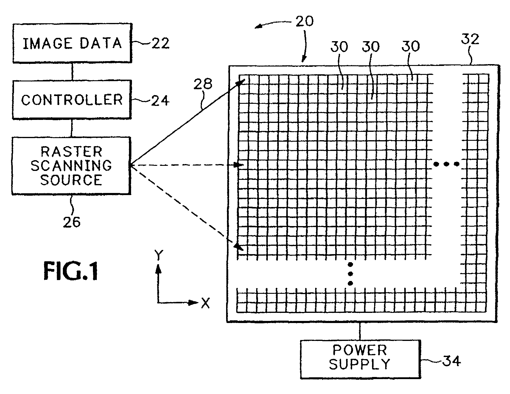
- FIG. 1 is a schematic diagram illustrating one embodiment of an optically addressable display system.
- FIG. 2 is a block diagram of one embodiment of an optically addressable display cell.
- FIG. 3 is a timing diagram illustrating an example of desired light output and actual light output in one embodiment of an optically addressable display system.
- FIG. 4 is a simplified block diagram of one embodiment of an optically addressable display cell.
- FIG. 5 illustrates a circuit for one embodiment of an optically addressable display cell.
- FIG. 6 illustrates a circuit for one embodiment of an optically addressable display cell.
- FIG. 7 is a timing diagram illustrating anexample of desired light output and actual light output in one embodiment of an optically addressable display system.
- FIG. 8 illustrates a circuit for one embodiment of an optically addressable display cell.
- FIG. 9 illustrates a circuit for one embodiment of an optically addressable display cell.
- FIG. 10 illustrates a possible flow chart of actions which may be performed by an optically addressable display system.
- FIG. 11 is a timing diagram illustrating an example of desired light output and actual light output in one embodiment of an optically addressable display system.
- FIG. 1 illustrates an optically addressable display system 20.
- Image data 22 is provided to a controller 24 by a linked host, such as a computer, projector, network connection, personal digital assistant, or other electronic device (not shown).
- the controller 24 processes the image data 22 into a format which is compatible with raster scanning source 26.
- Raster scanning source 26 emits at least one raster light beam 28, and can accurately direct this raster light beam 28 in the Y-axis direction, the X-axis direction, or any combination thereof, so that the raster light beam can fall onto any of the optically addressable display cells 30 which make up the display 32 of the optically addressable display system 20.
- the display 32 has at least one set of conductors which are configured to receive a voltage and a ground, and is connected to a power supply 34.
- the display 32 does not, however, need to be connected to control lines, since the control signals may be transmitted optically from the raster scanning source 26.
- the raster scanning source 26 can be implemented with one or more light emitting diodes or one or more laser sources, coupled with a controllable light deflecting surface or other positioning means to position the raster light beam 28 onto a desired optically addressable display cell 30.
- the raster scanning source 26 turns the raster light beam 28 on or off when aimed at a given optically addressable display cell 30, depending on whether there is image data 22 to display at that optically addressable display cell 30, and depending on the cell's 30 design and operation.
- FIG. 2 illustrates possible designs for an optically addressable display cell or pixel 30 with a block diagram.
- the optically addressable display cell 30 has a light sensor 36 which is sensitive to light from the raster light beam 28.
- the light sensor 36 can be constructed from a photodiode, phototransistor, or any other light sensitive component or device.
- the light sensor 36 is coupled to at least one display element 38.
- the display element 38 may be designed to emit, pass, or reflect light at any desired wavelength, for example, the display element 38 may emit, pass, or reflect light which is red, blue, green, cyan, magenta, yellow, white, infrared, or even ultra-violet.
- the display element 38 will be discussed as being constructed from a light emitting diode (LED) and therefore able to emit light, but any light generating element, controllable light reflecting element, or controllable aperture element would be acceptable provided it fit into a desired size criteria for the optically addressable display cell 30.
- the display element 38 or elements 38 in an optically addressable display cell 30 are designed to emit light which can be combined with light from other optically addressable display cells 30 to form an image on the display 32 which is representative of the image data 22.
- the optically addressable display cell 30 can be designed to emit light 40 from the display element 38 when the raster light beam 28 is positioned to activate the light sensor 36 and to not emit light 40 when there is no incident raster light beam28.
- the optically addressable display cell 30 may also be designed to work in the opposite fashion, in other words: emit light 40 from display element 38 when there is no incident light 28 on the light sensor 36, and not emit light 40 when there is incident light 28 on the light sensor 36.
- this specification will describe the former case, where an incident raster light beam 28 on the light sensor 36 causes the display element 38 to emit light 40. It should be understood, however, that an inverted operation is possible and intended to be covered by this specification.
- Optically addressable display cells 30 may have more than one display element 38.
- the raster scanning source 26 will cause a raster light beam 28 to fall on a given light sensor 36 in a manner which communicates more than one element of image data.
- the raster light beam may be turned on, off, and then on again during one pass of the optically addressable display cell 30.
- the optically addressable display cell 30 utilizes decoding circuitry 42 to separate the raster light beam 28 "on” and “off' states detected by the light sensor 36 and route the appropriate on/off signal to the display elements 38.
- decoding circuitry 42 may be implemented in an optically addressable display cell 30, a cell with one display element 38 tied to the light sensor 36, will be used for the sake of simplicity and discussion.
- FIG. 3 illustrates a timing diagram of how the optically addressable display cell 30 might operate in an optically addressable display system 20. Since the raster scanning source 26 must scan its raster light beam 28 across multiple optically addressable display cells 30, there will be a scanning duty cycle 46 for a given optically addressable display cell 30. During the active portions 48A-48E of the scanning duty cycle 46, the raster scanning source 26 has an opportunity to activate the raster light beam 28 so that it can be detected by the light sensor 36 in the optically addressable display cell 30. During the inactive portions 50 of the scanning duty cycle 46, the raster light beam 28 can not contact the optically addressable display cell 30. The controller 24 processes the image data 22 to determine the desired light output 52 for given optically addressable display cell 30 over time. The desired light output curve 52 in FIG. 3 shows that the desired light output can be either on or off.
- Raster light beam activation curve 54 illustrates how this works with respectto the scanning duty cycle 46 and the desired light output 52 over time.
- the raster light beam activation curve 54 shows that the raster light beam 28 is activated 56A during the active portion 48A. Since the display element 38 in the optically addressable display cell 30 of FIG.
- the actual light output 58 graphed in FIG. 3 tracks the raster light beam activation curve 54. This results in an off period 60A where the actual light output 58 is turned off, despite the fact that the desired light output 52 is on for the same corresponding off period 60A.
- the raster scanning source 26 has an opportunity to activate the actual light output again if desired.
- the desired light output 52 is on during the active portion 48B.
- the raster light beam 28 is activated 56B and actual light output 58 is turned on only during the active portion 48B.
- the raster scanning source will again have an opportunity to activate the raster light beam 28, and therefore the actual light output 58.
- the desired light output 52 is off, so, as curve 54 shows, the raster light beam 28 is not activated during active portion 48C.
- the actual light output 58 is off during the active portion 48C. Note that during the time frame 62, which began with active portion 48C, the actual light output 58 exactly tracks the desired light output 52.
- FIG. 4 illustrates, in block-diagram format, an embodiment of an optically addressable display cell 44 which is able to mitigate or eliminate the diminished perceived brightness in an optically addressable display system 20.
- the optically addressable display cell has a light sensor 36 coupled to a display element 38.
- a memory 45 is also coupled to the light sensor. The memory allows the display element 38 to remain turned on for a period after the light sensor 36 has stopped receiving the raster light beam 28.
- FIG. 5 illustrates an embodiment of an optically addressable display cell 66 which is able to mitigate or eliminate the diminished perceived brightness in an optically addressable display system 20.
- the optically addressable display cell 66 has a light sensor which is photo diode 68.
- the anode of the photo diode 68 (light sensor input) is coupled to a conductor which is configured to receive a voltage, and, as shown, is connected to a first positive voltage V A + 70.
- the cathode of photo diode 68 (light sensor output) is connected to the gate of a field effect transistor (FET) 72.
- FET field effect transistor
- the photo diode 68 is a light sensor, and other types of light sensing means could be used in place of photo diode 68, for example, but not limited to, photo transistor 69.
- Photo transistor 69 could be used in place of photo diode 68 by removing the photo diode 68 and connecting the collector of photo transistor 69 where the anode of photo diode 68 was, and the emitter of the photo transistor 69 where the cathode of the photo diode was.
- the drain of FET 72 is connected to a second positive voltage V B + 74.
- V A + 70 and V B + 74 may be different or the same, depending on the desired implementation.
- the source of FET 72 is coupled to a display element, here shown as a light emitting diode (LED) 76.
- LED light emitting diode
- the source of FET 72 is connected to the anode of the LED 76 (display element input).
- the cathode of LED 76 (display element output) is coupled to a conductor which is configured to receive a ground, and as shown is connected to a ground 78.
- An energy storage element, such as capacitor 80, is connected between the cathode of photo diode 68 and the cathode of LED 76.
- the capacitor 80 is an example of the memory 45 from FIG. 4.
- a resistor 82 may also be connected between the cathode of pho to diode 68 and the cathode of LED 76.
- this embodiment shows an FET 72, other types of transistors, such as P-type transistors, or even a relay could be used.
- the FET 72 is effectively a switch where the gate is like a selector, the drain is like an input, and the source is like an output. When the selector is activated, the input is connected to the output. When the selector is deactivated, the input is disconnected from the output.
- switching means for example, but not limited to various transistors and relays which can function like this type of switch.
- the LED 76 could be connected on the drain side of FET 72, with the cathode of LED 76 connected to the drain of FET 72, and the anode of LED 76 connected to V B + 74.
- the source of FET 72 would be connected to ground 78
- the capacitor 80 would be connected between the cathode of photo diode 68 and ground 78.
- the resistor 82 could also be connected between the cathode of photo diode 68 and ground 78.
- the capacitor 80 When the raster light beam 28 illuminates the photo diode 68, the capacitor 80 is charged by current flowing through the photo diode 68. The resulting voltage on the capacitor 80 is communicated to the gate of the FET 72. This causes current to flow through the FET 72 and through the LED 76, causing the LED 76 to emit light 40. When the raster light beam 28 stops illuminating the photo diode 68, current stops flowing through the photo diode 68. The capacitor 80, however, still initially has a charge stored in it, and the FET 72 will remain on until the charge on the capacitor 80 is substantially discharged, or dissipated below the turn-on threshold for the FET 72. Once the voltage on the capacitor 80 drops below the threshold for the FET 72, the FET 72 stops conducting current and the LED 76 stops emitting.
- the capacitor 80 may be discharged through the gate of FET 72 in an FET 72 selected with a controlled amount of gate leakage.
- the capacitor 80 may also be discharged through the optional resistor 82.
- the RC circuit formed by the capacitor 80 and the gate leakage of FET 72 or by the capacitor 80 and the resistor 82 is preferably designed so that the "on time" for FET 72 (and therefore the LED 76) approximately matches the length of time between scans of the raster light beam 28, or the period of time 60A shown in FIG. 3. This helps the actual light output 58 (FIG. 3) more closely resemble the desired light output 52 (FIG. 3), thereby reducing or eliminating the diminished perceived brightness.
- FIG. 6 illustrates an embodiment of an optically addressable display cell 84 which is also able to mitigate or eliminate the diminished perceived brightness in an optically addressable display system 20.
- the optically addressable display cell 84 has a photo diode 68.
- the anode of the photo diode 68 is connected to a first positive voltage V A + 70.
- the cathode of photo diode 68 is connected to the gate of a field effect transistor (FET) 86.
- the source of FET 86 is connected to a ground 78.
- the drain of FET 86 is connected to the cathode of a light emitting diode (LED) 76.
- the anode of LED 76 is connected to a second positive voltage V B + 74.
- V A + 70 and V B + 74 may be different or the same, depending on the desired implementation.
- FET 86 is chosen for a particular gate capacitance 88 between the gate and the source.
- the gate capacitance is an example of an energy storage element, or more generally, a memory 45.
- a resistor 82 may also be connected between the cathode of photo diode 68 and ground 78.
- the gate capacitance 88 which takes the place of capacitor 80 from FIG. 5, is charged by current flowing through the photo diode 68.
- the resulting voltage on the gate capacitance 88, in FIG. 6, is present on the gate of the FET 86. This causes current to flow through LED 76 and through FET 86, causing the LED 76 to emit light 40.
- the raster light beam 28 stops illuminating the photo diode 68, current stops flowing through the photo diode 68.
- the gate capacitance 88 still initially has a charge stored in it, and the FET 86 will remain on until the charge on the capacitance 88 is dissipated below the turn-on threshold for the FET 86. Once the voltage on the gate capacitance 88 drops below the threshold for the FET 86, the FET 86 stops conducting current and the LED 76 stops emitting. When the photo diode 68 is off, the gate capacitance 88 may be discharged through gate leakage of FET 86. The gate capacitance 88 may also be discharged through optional resistor 82.
- the RC circuit formed by the gate capacitance 88 and the resistance of FET 86 gate leakage or by the gate capacitance 88 and the resistor 82 is preferably designed so that the "on time" for FET 86 (and therefore the LED 76) approximately matches the length of time between scans of the raster light beam 28, or the period of time 60A shown in FIG. 3. This helps the actual light output 58 (FIG. 3) more closely resemble the desired light output 52 (FIG. 3), thereby reducing or eliminating the diminished perceived brightness.
- FIG. 7 illustrates a timing diagram of how the optically addressable display cells 66 and 84 (from FIGS. 5 and 6) might operate in an optically addressable display system. Since the raster scanning source 26 must scan its raster light beam 28 across multiple optically addressable display cells 66, 84, there will be a scanning duty cycle 90 for a given optically addressable display cell 66, 84. During the active portions 92A-92E of the scanning duty cycle 90, the raster scanning source 26 has an opportunity to activate the raster light beam 28 so that it can be detected by the photo diode 68 in the optically addressable display cell 66, 84.
- the raster light beam 28 can not contact the optically addressable display cell 66, 84.
- the controller 24 processes the image data 22 to determine the desired light output 96 for given optically addressable display cell 66, 84 over time.
- the desired light output 96 curve in FIG. 7 shows that the desired light output can be either on or off.
- Raster light beam activation curve 98 illustrates how this works with respect to the scanning duty cycle 90 and the desired light output 96 over time.
- the raster light beam activation curve 98 shows that the raster light beam 28 is activated 100 during the active portion 92A.
- the reduced off period 110 means that the actual light output curve 102 is more closely tracking the desired light emission curve 96.
- the off period 110 can be reduced further, or even eliminated by choosing capacitor 80, FET 72, and optionally resistor 82 such that LED 76 remains on for a longer duration.
- the off period 110 can be reduced further, or even eliminated by choosing FET 86 with gate capacitance 88 and optionally resistor 82 such that LED 76 remains on for a longer duration.
- the actual component values chosen will depend on the embodiment used and can be determined by those skilled in the art depending on the entire system parameters.
- the embodiments illustrated in FIGS. 5 and 6 enable a reduction of the off period 110 shown in FIG. 7. Reducing the off period 110 increases the perceived brightness of the optically addressable display system 20.
- FIG. 8 illustrates an embodiment of an optically addressable display cell 112 which, in conjunction with an appropriate process, is able to eliminate or nearly eliminate the diminished perceived brightness in an optically addressable display system 20.
- the optically addressable display cell 112 has a photo diode 68.
- the anode of the photo diode 68 is connected to a first positive voltage V A + 70.
- the cathode of the photo diode 68 is connected to an input 114 of a static latch, or toggle flip- flop 116.
- This static latch, or state machine is one example of the memory 45 of FIG. 4.
- a voltage ground 78 is connected to the toggle flip-flop 116 as well.
- a pull-up resistor 118 is connected between the voltage V A + 70 and a reset point 120 on the toggle flip-flop 116.
- V A + 70 When power is initially applied to the optically addressable display cell 112, the voltage V A + 70 will create a transitioning edge which will reset the toggle flip -flop 116 to a known state.
- the controller 24 in the optically addressable display system 20 must always know the previous state of each optically addressable display cell 112. Providing a reset signal to each cell 112 assures that the controller 24 will know the starting state for each cell 112.
- the reset point 120 on the toggle flip-flop 116 is illustrated as being controlled from a pull-up resistor 118 connected to the voltage V A + 70, there are other ways to provide this signal which will be apparent to those skilled in the art. This specification is intended to cover these functionally equivalent methods of providing a reset signal, including, but not limited to, pull-down connections and a separate reset line from the controller 24 to all of the optically addressable display cells 112.
- An output 122 of the toggle flip-flop 116 is connected to the anode of the LED 76, and the cathode of LED 76 is connected to ground 78.
- This embodiment requires that the output 122 of the toggle flip -flop 116 is sufficient to drive the LED 76 when the voltage at the output 122 is active.
- Other means for toggling an output with an input will be apparent to those skilled in the art, and may be implemented in lieu of the toggle flip-flop 116, including, but not limited to discrete logic component flip-flop equivalents. Such state machines, and means for toggling an output with an input are intended to be covered by this specification.
- operation occurs as follows: Since a toggle flip-flop 116 is involved, knowledge of the previous flip-flop state is required. For the sake of explanation, the previous state of the output 122 will be off. When the raster light beam 28 contacts the photo diode 68, the photo diode 68 will conduct current. This creates a positive voltage transition at the input 114 of the toggle flip-flop 116. The positive voltage transition causes the toggle flip-flop 116 to change the state of the output 122 from off to on. The voltage created at the output 122 in the on state causes current to flow in the LED 76, thereby causing it to emit light 40.
- the photo diode 68 When the raster light beam 28 ceases to contact the photo diode 68, the photo diode 68 will stop conducting current. This causes a negative voltage transition at the input 114 of the toggle flip-flop 116. The toggle flip- flop 116 does not react to a negative voltage transition, so the output 122 remains on, and the LED 76 remains on. The LED 76 will remain turned on until the raster light beam 28 is incident on the photo diode 68 again. When the raster light beam 28 falls on the photo diode 68 the next time, the photo diode 68 will begin to conduct current. This creates a positive voltage transition at the input 114 of the toggle flip-flop 116. The positive voltage transition causes the toggle flip-flop 116 to change the state of the output 122 from on to off. Since there is no voltage at the output 122, no current flows through the LED 76, and no light is emitted from the LED 76.
- FIG. 9 illustrates an embodiment of an optically addressable display cell 124 which, in conjunction with an appropriate process, is able to eliminate or nearly eliminate the diminished perceived brightness in an optically addressable display system 20.
- the optically addressable display cell 124 has a photo diode 68.
- the anode of the photo diode 68 is connected to a first positive voltage V A + 70.
- the cathode of the photo diode 68 is connected to an input 114 of a static latch, or toggle flip- flop 116.
- This static latch, or state machine is one example of the memory 45 of FIG. 4.
- a voltage ground 78 is connected to the toggle flip-flop 116.
- a pull-up resistor 118 is connected between the voltage V A + 70 and a reset point 120 on the toggle flip -flop 116.
- the voltage V A + 70 will create a transitioning edge which will reset the toggle flip- flop 116 to a known state.
- the controller 24 in the optically addressable display system 20 must always know the previous state of each optically addressable display cell 124. Providing a reset signal to each cell 124 assures that the controller 24 will know the starting state for each cell 124.
- the reset point 120 on the toggle flip-flop 116 is illustrated as being controlled from a pull-up resistor 118 connected to the voltage V A + 70, there are other ways to provide this signal which will be apparent to those skilled in the art. This specification is intended to cover these functionally equivalent methods of providing a reset signal, including, but not limited to, pull-down connections and a separate reset line from the controller 24 to all of the optically addressable display cells 124.
- the output 122 of the toggle flip-flop 116 is connected to the gate of FET 126.
- the drain of FET 126 is connected to a second voltage V B + 128.
- the source of the FET 126 is connected to the anode of the LED 76, and the cathode of LED 76 is connected to ground 78.
- This embodiment requires that the output 122 of the toggle flip-flop 116 is sufficient to turn on the FET 126 when the voltage at the output 122 is active. When the FET 126 is turned on, current will flow from V B + 128 through the LED 76, and light 40 will be emitted.
- the LED 76 which does not have an FET, allows the LED 76 to be driven by a different voltage than that which supplies the toggle flip-flop 116, thereby allowing V A + 70 and V B + 128 to be different or, if V A + 70 and V B + 128 are the same, to at least avoid loading the toggle flip-flop 116 with the current which will pass through LED 76.
- this embodiment shows an FET 126, other types of transistors, such as p-type transistors, or even a relay could be used.
- the FET 126 is effectively a switch where the gate is like a selector, the drain is like an input, and the source is like an output. When the selector is activated, the input is connected to the output.
- the light emitter 76 could be connected on the drain side of FET 126, with the cathode of LED 76 connected to the drain of FET 126, and the anode of LED 76 connected to V B + 128. In this case, the source of FET 126 would be connected to ground 78.
- the photo diode 68 When the raster light beam 28 ceases to contact the photo diode 68, the photo diode 68 will stop conducting current. This causes a negative voltage transition at the input 114 of the toggle flip-flop 116.
- the toggle flip -flop 116 does not react to a negative voltage transition, so the output 122 remains on, the FET 126 remains on, and the LED 76 remains on.
- the LED 76 will remain turned on until the raster beam light 28 is incident on the photo diode 68 again.
- the photo diode 68 When the raster beam light 28 falls on the photo diode 68 the next time, the photo diode 68 will begin to conduct current. This creates a positive voltage transition at the input 114 of the toggle flip-flop 116.
- the positive voltage transition causes the toggle flip-flop 116 to change the state of the output 122 from on to off. Since there is no voltage at the output 122, the FET 126 turns off. When FET 126 is turned off, no current flows through the LED 76, and no light is emitted from the LED 76.
- FIG. 10 illustrates one embodiment of a process which may be used by an optically addressable display system 20 having optically addressable display cells, such as optically addressable display cells 112 and 124.
- the process requires that the controller 24 know the previous state for all of the optically addressable display cells 112, 124. This is accomplished when the optically addressable display system 20 is powered on 130. At power-on 130, the described reset function of the optically addressable display cells 112, 124 ensures that all of the LED's 76, or display elements are turned off.
- the controller 24 stores a corresponding value of "off" for each optically addressable display cell 112, 124.
- All of the optically addressable display cells 112, 124 in the optically addressable display system 20 will be scanned in turn by the raster scanning source 26.
- the process begins by indexing 132 the raster scanning source to the first optically addressable display cell.
- the optically addressable display cell onto which the raster scanning source is indexed is the "current cell”.
- the controller examines 134 the previous state for the current cell. If the previous state for the current cell is "on" 136, the controller examines 138 the new state desired for the current cell. If the new state is desired to remain "on” 140, the raster light beam will not be activated 142 over the current cell, thus allowing the current cell to remain on as in its previous state.
- the current state is stored 144 as the previous state of the current cell.
- the processor decides 146 if the raster scanning source is at the last optically addressable display cell in the optically addressable display system 20. If the raster scanning source is not 148 at the last optically addressable display cell, the raster scanning source is indexed 150 to a next optically addressable display cell. If the raster scanning source had been 152 at the last optically addressable display cell, the raster scanning source would have been indexed 132 to the first optically addressable display cell.
- the raster light beam will be activated 154 over the current cell, thus allowing the current cell to change from on to off.
- the current state is stored 144 as the previous state of the current cell, and the process continues as already described.
- a third path is where the previous state for a cell was "off", and the desired new state for the cell is "off'. In this case, after indexing the raster scanning source 132, 150 the controller examines 134 the previous state for the current cell. If the previous state for the current cell is "off' 156, the controller examines 158 the new state desired for the current cell.
- the controller examines 134 the previous state for the current cell. If the previous state for the current cell is "off' 156, the controller examines 158 the new state desired for the current cell.
- the raster light beam will be activated 154 over the current cell, thus allowing the current cell to change from off to on.
- the current state is stored 144 as the previous state of the current cell, and the process continues as already described.
- the process illustrated in FIG. 10 evaluates the previous state 134 for the current cell before evaluating 138, 158 the desired new state for the current cell, a process could clearly be set up to evaluate the desired new state for the current cell before the previous state.
- the decision to activate the raster light beam can also be looked at as the logical exclusive-or (XOR) comparison of the desired new state and the previous state of the current cell.
- FIG. 11 illustrates a possible timing chart for an optically addressable display system 20 which has optically addressable display cells, like the cells 112 or 124 in FIGS. 8 and 9 with a toggle flip-flop 116, and utilizing a process like the one illustrated in FIG. 10. Since the raster scanning source 26 must scan its raster light beam 28 across multiple optically addressable display cells 112, 124, there will be a scanning duty cycle 164 for a given optically addressable display cell 112, 124. During the active portions 166A- 166E of the scanning duty cycle 164, the raster scanning source 26 has an opportunity to activate the raster light beam 28 so that it can be detected by the photo diode 68 in the optically addressable display cell 112, 124.
- the raster light beam 28 can not contact the optically addressable display cell 112, 124.
- the controller 24 processes the image data 22 to determine the desired light output 170 for given optically addressable display cell 112, 124 over time.
- the desired light output 170 curve in FIG. 11 shows that the desired light output can be either on or off.
- the controller 24 compares the state of the optically addressable display cell on the previous cycle 172 with the desired light output state 170.
- the controller 24 may perform an exclusive - or (XOR) comparison or the equivalent of an XOR comparison of the desired light output 170 and the state of the optically addressable display cell on the previous cycle 172 for each active portion 166A- 166E of the scanning duty cycle 164.
- the raster light beam activation 174 during the active portions 166A- 166E of the scanning duty cycle 164 is the XOR of the desired light output 170 and the state of the optically addressable display cell on the previous cycle 172.
- the state of the actual light output 176 toggles with each rising edge of the raster light beam activation 174.
- the actual light output 176 exactly or almost exactly matches the desired light output 170 intended by the controller 24.
- This embodiment also has the advantage that it can work with different rates of a scanning duty cycle 164, without having to change the design of the optically addressable display cells 112, 124.
- An optically addressable display system 20 allows a display 32 to be constructed with minimal or no physical control lines connecting the display 32 to the controller 24.
- An optically addressable display system 20 provides a brighter image with less wasted energy than conventional liquid crystal or thin-film transistor active matrix displays.
Landscapes
- Engineering & Computer Science (AREA)
- Physics & Mathematics (AREA)
- Computer Hardware Design (AREA)
- General Physics & Mathematics (AREA)
- Theoretical Computer Science (AREA)
- Control Of Indicators Other Than Cathode Ray Tubes (AREA)
- Devices For Indicating Variable Information By Combining Individual Elements (AREA)
- Liquid Crystal (AREA)
- Control Of El Displays (AREA)
- Transforming Electric Information Into Light Information (AREA)
Abstract
Description
- Image displays may be formed by an array of optically addressable display cells. Each cell may have a light sensor coupled to a display element such as a light emitting diode (LED) or a light valve or light controlling surface which determines whether to let a certain light pass through it or reflect from it to a viewer. A voltage and electrical ground are provided to each cell, but no circuitry or physical contacts are required to connect the display to a display controller processing image data. Instead, control information is conveyed optically by projection. The array of optically addressable display cells is scanned in a raster fashion by at least one beam of light which has a wavelength or wavelengths which may be sensed by the light sensors in the optically addressable display cells. An example of such a method and apparatus for image and video display is described in co-pending U.S. patent application number 10/020,112, the specification of which is herein incorporated by reference.
- An optically addressable display system has the advantage of not requiring the control signals for each addressable display cell to be wired into the display. The display elements in an optically addressable display system may also be constructed to use significantly less energy than a light source such as an arc lamp or an incandescent lamp which are typical of many active matrix display screens which are currently available.
- Despite the many advantages of an optically addressable display system, continually brighter displays are often desired.
- FIG. 1 is a schematic diagram illustrating one embodiment of an optically addressable display system.
- FIG. 2 is a block diagram of one embodiment of an optically addressable display cell.
- FIG. 3 is a timing diagram illustrating an example of desired light output and actual light output in one embodiment of an optically addressable display system.
- FIG. 4 is a simplified block diagram of one embodiment of an optically addressable display cell.
- FIG. 5 illustrates a circuit for one embodiment of an optically addressable display cell.
- FIG. 6 illustrates a circuit for one embodiment of an optically addressable display cell.
- FIG. 7 is a timing diagram illustrating anexample of desired light output and actual light output in one embodiment of an optically addressable display system.
- FIG. 8 illustrates a circuit for one embodiment of an optically addressable display cell.
- FIG. 9 illustrates a circuit for one embodiment of an optically addressable display cell.
- FIG. 10 illustrates a possible flow chart of actions which may be performed by an optically addressable display system.
- FIG. 11 is a timing diagram illustrating an example of desired light output and actual light output in one embodiment of an optically addressable display system.
- FIG. 1 illustrates an optically
addressable display system 20.Image data 22 is provided to acontroller 24 by a linked host, such as a computer, projector, network connection, personal digital assistant, or other electronic device (not shown). Thecontroller 24 processes theimage data 22 into a format which is compatible withraster scanning source 26.Raster scanning source 26 emits at least oneraster light beam 28, and can accurately direct thisraster light beam 28 in the Y-axis direction, the X-axis direction, or any combination thereof, so that the raster light beam can fall onto any of the opticallyaddressable display cells 30 which make up thedisplay 32 of the opticallyaddressable display system 20. Thedisplay 32 has at least one set of conductors which are configured to receive a voltage and a ground, and is connected to apower supply 34. Thedisplay 32 does not, however, need to be connected to control lines, since the control signals may be transmitted optically from theraster scanning source 26. Theraster scanning source 26 can be implemented with one or more light emitting diodes or one or more laser sources, coupled with a controllable light deflecting surface or other positioning means to position theraster light beam 28 onto a desired opticallyaddressable display cell 30. Theraster scanning source 26 turns theraster light beam 28 on or off when aimed at a given opticallyaddressable display cell 30, depending on whether there isimage data 22 to display at that opticallyaddressable display cell 30, and depending on the cell's 30 design and operation. - FIG. 2 illustrates possible designs for an optically addressable display cell or
pixel 30 with a block diagram. The opticallyaddressable display cell 30 has alight sensor 36 which is sensitive to light from theraster light beam 28. Thelight sensor 36 can be constructed from a photodiode, phototransistor, or any other light sensitive component or device. Thelight sensor 36 is coupled to at least onedisplay element 38. Thedisplay element 38 may be designed to emit, pass, or reflect light at any desired wavelength, for example, thedisplay element 38 may emit, pass, or reflect light which is red, blue, green, cyan, magenta, yellow, white, infrared, or even ultra-violet. For simplicity of explanation, thedisplay element 38 will be discussed as being constructed from a light emitting diode (LED) and therefore able to emit light, but any light generating element, controllable light reflecting element, or controllable aperture element would be acceptable provided it fit into a desired size criteria for the opticallyaddressable display cell 30. Thedisplay element 38 orelements 38 in an opticallyaddressable display cell 30 are designed to emit light which can be combined with light from other opticallyaddressable display cells 30 to form an image on thedisplay 32 which is representative of theimage data 22. The opticallyaddressable display cell 30 can be designed to emitlight 40 from thedisplay element 38 when theraster light beam 28 is positioned to activate thelight sensor 36 and to not emitlight 40 when there is no incident raster light beam28. The opticallyaddressable display cell 30 may also be designed to work in the opposite fashion, in other words: emitlight 40 fromdisplay element 38 when there is noincident light 28 on thelight sensor 36, and not emitlight 40 when there isincident light 28 on thelight sensor 36. For simplicity, this specification will describe the former case, where an incidentraster light beam 28 on thelight sensor 36 causes thedisplay element 38 to emitlight 40. It should be understood, however, that an inverted operation is possible and intended to be covered by this specification. - Optically
addressable display cells 30 may have more than onedisplay element 38. In this case, theraster scanning source 26 will cause araster light beam 28 to fall on a givenlight sensor 36 in a manner which communicates more than one element of image data. For example, if an opticallyaddressable display cell 30 has red, blue, andgreen display elements 38, and the red display element is desired on, the blue display element is desired off, and the green display element is desired on, the raster light beam may be turned on, off, and then on again during one pass of the opticallyaddressable display cell 30. In this situation, the opticallyaddressable display cell 30 utilizesdecoding circuitry 42 to separate theraster light beam 28 "on" and "off' states detected by thelight sensor 36 and route the appropriate on/off signal to thedisplay elements 38. Althoughmultiple display elements 38 anddecoding circuitry 42 may be implemented in an opticallyaddressable display cell 30, a cell with onedisplay element 38 tied to thelight sensor 36, will be used for the sake of simplicity and discussion. - FIG. 3 illustrates a timing diagram of how the optically
addressable display cell 30 might operate in an opticallyaddressable display system 20. Since theraster scanning source 26 must scan itsraster light beam 28 across multiple opticallyaddressable display cells 30, there will be ascanning duty cycle 46 for a given opticallyaddressable display cell 30. During theactive portions 48A-48E of thescanning duty cycle 46, theraster scanning source 26 has an opportunity to activate theraster light beam 28 so that it can be detected by thelight sensor 36 in the opticallyaddressable display cell 30. During theinactive portions 50 of thescanning duty cycle 46, theraster light beam 28 can not contact the opticallyaddressable display cell 30. Thecontroller 24 processes theimage data 22 to determine the desiredlight output 52 for given opticallyaddressable display cell 30 over time. The desiredlight output curve 52 in FIG. 3 shows that the desired light output can be either on or off. - During a given
active portion 48A-48E of thescanning duty cycle 46, if the corresponding desiredlight output 52 should be on, then theraster light beam 28 will be activated for the duration of that corresponding scanning duty cycleactive portion 48A-48E. Raster lightbeam activation curve 54 illustrates how this works with respectto thescanning duty cycle 46 and the desiredlight output 52 over time. In the example shown in FIG. 3, for theactive portion 48A of the scanning duty cycle, the desiredlight output 52 state is on. Therefore, the raster lightbeam activation curve 54 shows that theraster light beam 28 is activated 56A during theactive portion 48A. Since thedisplay element 38 in the opticallyaddressable display cell 30 of FIG. 2 is only emitting when there is incident light on thelight sensor 36, theactual light output 58 graphed in FIG. 3 tracks the raster lightbeam activation curve 54. This results in an offperiod 60A where theactual light output 58 is turned off, despite the fact that the desiredlight output 52 is on for the same corresponding offperiod 60A. At the nextactive portion 48B of thescanning duty cycle 46, theraster scanning source 26 has an opportunity to activate the actual light output again if desired. As the example of FIG. 3 shows, the desiredlight output 52 is on during theactive portion 48B. Thus, duringactive portion 48B, theraster light beam 28 is activated 56B andactual light output 58 is turned on only during theactive portion 48B. Again, there is an offperiod 60B where the desired light output is on, but where the actual light output is off. At the next active portion, 48C of the scanning duty cycle, the raster scanning source will again have an opportunity to activate theraster light beam 28, and therefore theactual light output 58. For theactive portion 48C, however, the desiredlight output 52 is off, so, ascurve 54 shows, theraster light beam 28 is not activated duringactive portion 48C. Correspondingly, theactual light output 58 is off during theactive portion 48C. Note that during thetime frame 62, which began withactive portion 48C, the actuallight output 58 exactly tracks the desiredlight output 52. Thus, there will be no off period during the time the desiredlight output 52 is off, but for times when the desiredlight output 52 is on, there will be offperiods 60A-60C when the actuallight output 58 is turned off. This limited actual on-time 56A-56C, when compared to anentire duty cycle 64A-64C results in a diminished perceived brightness of thedisplay 32. - FIG. 4 illustrates, in block-diagram format, an embodiment of an optically
addressable display cell 44 which is able to mitigate or eliminate the diminished perceived brightness in an opticallyaddressable display system 20. The optically addressable display cell has alight sensor 36 coupled to adisplay element 38. Amemory 45 is also coupled to the light sensor. The memory allows thedisplay element 38 to remain turned on for a period after thelight sensor 36 has stopped receiving theraster light beam 28. - FIG. 5 illustrates an embodiment of an optically
addressable display cell 66 which is able to mitigate or eliminate the diminished perceived brightness in an opticallyaddressable display system 20. The opticallyaddressable display cell 66 has a light sensor which isphoto diode 68. The anode of the photo diode 68 (light sensor input) is coupled to a conductor which is configured to receive a voltage, and, as shown, is connected to a firstpositive voltage V A + 70. The cathode of photo diode 68 (light sensor output) is connected to the gate of a field effect transistor (FET) 72. - The
photo diode 68 is a light sensor, and other types of light sensing means could be used in place ofphoto diode 68, for example, but not limited to,photo transistor 69.Photo transistor 69 could be used in place ofphoto diode 68 by removing thephoto diode 68 and connecting the collector ofphoto transistor 69 where the anode ofphoto diode 68 was, and the emitter of thephoto transistor 69 where the cathode of the photo diode was. - The drain of
FET 72 is connected to a secondpositive voltage V B + 74.V A + 70 andV B + 74 may be different or the same, depending on the desired implementation. The source ofFET 72 is coupled to a display element, here shown as a light emitting diode (LED) 76. Specifically, the source ofFET 72 is connected to the anode of the LED 76 (display element input). The cathode of LED 76 (display element output) is coupled to a conductor which is configured to receive a ground, and as shown is connected to aground 78. An energy storage element, such ascapacitor 80, is connected between the cathode ofphoto diode 68 and the cathode ofLED 76. Thecapacitor 80 is an example of thememory 45 from FIG. 4. Optionally, aresistor 82 may also be connected between the cathode of pho todiode 68 and the cathode ofLED 76. Although this embodiment shows anFET 72, other types of transistors, such as P-type transistors, or even a relay could be used. TheFET 72 is effectively a switch where the gate is like a selector, the drain is like an input, and the source is like an output. When the selector is activated, the input is connected to the output. When the selector is deactivated, the input is disconnected from the output. Those skilled in the art can appreciate that there are many switching means, for example, but not limited to various transistors and relays which can function like this type of switch. This disclosure is intended to include such functional equivalents and substitutions. Alternatively, theLED 76 could be connected on the drain side ofFET 72, with the cathode ofLED 76 connected to the drain ofFET 72, and the anode ofLED 76 connected toV B + 74. In this case, the source ofFET 72 would be connected to ground 78, and thecapacitor 80 would be connected between the cathode ofphoto diode 68 andground 78. In this alternate embodiment, theresistor 82 could also be connected between the cathode ofphoto diode 68 andground 78. - When the
raster light beam 28 illuminates thephoto diode 68, thecapacitor 80 is charged by current flowing through thephoto diode 68. The resulting voltage on thecapacitor 80 is communicated to the gate of theFET 72. This causes current to flow through theFET 72 and through theLED 76, causing theLED 76 to emit light 40. When theraster light beam 28 stops illuminating thephoto diode 68, current stops flowing through thephoto diode 68. Thecapacitor 80, however, still initially has a charge stored in it, and theFET 72 will remain on until the charge on thecapacitor 80 is substantially discharged, or dissipated below the turn-on threshold for theFET 72. Once the voltage on thecapacitor 80 drops below the threshold for theFET 72, theFET 72 stops conducting current and theLED 76 stops emitting. - When the
photo diode 68 is off, thecapacitor 80 may be discharged through the gate ofFET 72 in anFET 72 selected with a controlled amount of gate leakage. Thecapacitor 80 may also be discharged through theoptional resistor 82. The RC circuit formed by thecapacitor 80 and the gate leakage ofFET 72 or by thecapacitor 80 and theresistor 82 is preferably designed so that the "on time" for FET 72 (and therefore the LED 76) approximately matches the length of time between scans of theraster light beam 28, or the period oftime 60A shown in FIG. 3. This helps the actual light output 58 (FIG. 3) more closely resemble the desired light output 52 (FIG. 3), thereby reducing or eliminating the diminished perceived brightness. - FIG. 6 illustrates an embodiment of an optically
addressable display cell 84 which is also able to mitigate or eliminate the diminished perceived brightness in an opticallyaddressable display system 20. The opticallyaddressable display cell 84 has aphoto diode 68. The anode of thephoto diode 68 is connected to a firstpositive voltage V A + 70. The cathode ofphoto diode 68 is connected to the gate of a field effect transistor (FET) 86. The source ofFET 86 is connected to aground 78. The drain ofFET 86 is connected to the cathode of a light emitting diode (LED) 76. The anode ofLED 76 is connected to a secondpositive voltage V B + 74.V A + 70 andV B + 74 may be different or the same, depending on the desired implementation.FET 86 is chosen for aparticular gate capacitance 88 between the gate and the source. The gate capacitance is an example of an energy storage element, or more generally, amemory 45. Optionally, aresistor 82 may also be connected between the cathode ofphoto diode 68 andground 78. - In the embodiment illustrated in FIG. 6, when the
raster light beam 28 illuminates thephoto diode 68, thegate capacitance 88, which takes the place ofcapacitor 80 from FIG. 5, is charged by current flowing through thephoto diode 68. The resulting voltage on thegate capacitance 88, in FIG. 6, is present on the gate of theFET 86. This causes current to flow throughLED 76 and throughFET 86, causing theLED 76 to emit light 40. When theraster light beam 28 stops illuminating thephoto diode 68, current stops flowing through thephoto diode 68. Thegate capacitance 88, however, still initially has a charge stored in it, and theFET 86 will remain on until the charge on thecapacitance 88 is dissipated below the turn-on threshold for theFET 86. Once the voltage on thegate capacitance 88 drops below the threshold for theFET 86, theFET 86 stops conducting current and theLED 76 stops emitting. When thephoto diode 68 is off, thegate capacitance 88 may be discharged through gate leakage ofFET 86. Thegate capacitance 88 may also be discharged throughoptional resistor 82. The RC circuit formed by thegate capacitance 88 and the resistance ofFET 86 gate leakage or by thegate capacitance 88 and theresistor 82 is preferably designed so that the "on time" for FET 86 (and therefore the LED 76) approximately matches the length of time between scans of theraster light beam 28, or the period oftime 60A shown in FIG. 3. This helps the actual light output 58 (FIG. 3) more closely resemble the desired light output 52 (FIG. 3), thereby reducing or eliminating the diminished perceived brightness. - FIG. 7 illustrates a timing diagram of how the optically
addressable display cells 66 and 84 (from FIGS. 5 and 6) might operate in an optically addressable display system. Since theraster scanning source 26 must scan itsraster light beam 28 across multiple opticallyaddressable display cells scanning duty cycle 90 for a given opticallyaddressable display cell active portions 92A-92E of thescanning duty cycle 90, theraster scanning source 26 has an opportunity to activate theraster light beam 28 so that it can be detected by thephoto diode 68 in the opticallyaddressable display cell inactive portions 94 of thescanning duty cycle 90, theraster light beam 28 can not contact the opticallyaddressable display cell controller 24 processes theimage data 22 to determine the desiredlight output 96 for given opticallyaddressable display cell light output 96 curve in FIG. 7 shows that the desired light output can be either on or off. - During a given
active portion 92A-92E of thescanning duty cycle 90, if the corresponding desiredlight output 96 should be on, then theraster light beam 28 will be activated for the duration of that corresponding scanning duty cycleactive portion 92A-92E. Raster lightbeam activation curve 98 illustrates how this works with respect to thescanning duty cycle 90 and the desiredlight output 96 over time. In the example shownin FIG. 7, for theactive portion 92A of the scanning duty cycle, the desiredlight output 96 state is on. Therefore, the raster lightbeam activation curve 98 shows that theraster light beam 28 is activated 100 during theactive portion 92A. TheLED 76 in the opticallyaddressable display cells photo diode 68, so the actuallight output 102 graphed in FIG. 7 turns on 104 when the raster lightbeam activation curve 98 is turned on 100. The raster lightbeam activation curve 98 will necessarily turn off 106 at the completion of theactive portion 92A of thescanning duty cycle 90. The design of the opticallyaddressable display cells light output 102 to remain turned on during period 108, even after the raster light beam has been turned off 106. This results in a reduced offperiod 110, as compared to the larger offperiod 60A in FIG. 4. The reduced offperiod 110 means that the actuallight output curve 102 is more closely tracking the desiredlight emission curve 96. In the case of the opticallyaddressable display cell 66 embodied in FIG. 5, theoff period 110 can be reduced further, or even eliminated by choosingcapacitor 80,FET 72, and optionally resistor 82 such thatLED 76 remains on for a longer duration. In the case of the opticallyaddressable display cell 84 embodied in FIG. 6, theoff period 110 can be reduced further, or even eliminated by choosingFET 86 withgate capacitance 88 and optionally resistor 82 such thatLED 76 remains on for a longer duration. The actual component values chosen will depend on the embodiment used and can be determined by those skilled in the art depending on the entire system parameters. The embodiments illustrated in FIGS. 5 and 6 enable a reduction of theoff period 110 shown in FIG. 7. Reducing theoff period 110 increases the perceived brightness of the opticallyaddressable display system 20. - FIG. 8 illustrates an embodiment of an optically
addressable display cell 112 which, in conjunction with an appropriate process, is able to eliminate or nearly eliminate the diminished perceived brightness in an opticallyaddressable display system 20. The opticallyaddressable display cell 112 has aphoto diode 68. The anode of thephoto diode 68 is connected to a firstpositive voltage V A + 70. The cathode of thephoto diode 68 is connected to aninput 114 of a static latch, or toggle flip-flop 116. This static latch, or state machine, is one example of thememory 45 of FIG. 4. Avoltage ground 78 is connected to the toggle flip-flop 116 as well. A pull-upresistor 118 is connected between thevoltage V A + 70 and areset point 120 on the toggle flip-flop 116. When power is initially applied to the opticallyaddressable display cell 112, thevoltage V A +70 will create a transitioning edge which will reset the toggle flip -flop 116 to a known state. For this embodiment to work properly, thecontroller 24 in the opticallyaddressable display system 20 must always know the previous state of each opticallyaddressable display cell 112. Providing a reset signal to eachcell 112 assures that thecontroller 24 will know the starting state for eachcell 112. Although thereset point 120 on the toggle flip-flop 116 is illustrated as being controlled from a pull-upresistor 118 connected to thevoltage V A + 70, there are other ways to provide this signal which will be apparent to those skilled in the art. This specification is intended to cover these functionally equivalent methods of providing a reset signal, including, but not limited to, pull-down connections and a separate reset line from thecontroller 24 to all of the opticallyaddressable display cells 112. - An
output 122 of the toggle flip-flop 116 is connected to the anode of theLED 76, and the cathode ofLED 76 is connected to ground 78. This embodiment requires that theoutput 122 of the toggle flip -flop 116 is sufficient to drive theLED 76 when the voltage at theoutput 122 is active. Other means for toggling an output with an input will be apparent to those skilled in the art, and may be implemented in lieu of the toggle flip-flop 116, including, but not limited to discrete logic component flip-flop equivalents. Such state machines, and means for toggling an output with an input are intended to be covered by this specification. - At the level of the optically
addressable display cell 112, operation occurs as follows: Since a toggle flip-flop 116 is involved, knowledge of the previous flip-flop state is required. For the sake of explanation, the previous state of theoutput 122 will be off. When theraster light beam 28 contacts thephoto diode 68, thephoto diode 68 will conduct current. This creates a positive voltage transition at theinput 114 of the toggle flip-flop 116. The positive voltage transition causes the toggle flip-flop 116 to change the state of theoutput 122 from off to on. The voltage created at theoutput 122 in the on state causes current to flow in theLED 76, thereby causing it to emit light 40. When theraster light beam 28 ceases to contact thephoto diode 68, thephoto diode 68 will stop conducting current. This causes a negative voltage transition at theinput 114 of the toggle flip-flop 116. The toggle flip-flop 116 does not react to a negative voltage transition, so theoutput 122 remains on, and theLED 76 remains on. TheLED 76 will remain turned on until theraster light beam 28 is incident on thephoto diode 68 again. When theraster light beam 28 falls on thephoto diode 68 the next time, thephoto diode 68 will begin to conduct current. This creates a positive voltage transition at theinput 114 of the toggle flip-flop 116. The positive voltage transition causes the toggle flip-flop 116 to change the state of theoutput 122 from on to off. Since there is no voltage at theoutput 122, no current flows through theLED 76, and no light is emitted from theLED 76. - It should be apparent that a flip -flop could be chosen to react to a negative voltage transition instead of a positive voltage transition, as such modifications are within the abilities of those skilled in the art. Such equivalents are intended to be within the scope of this specification. Based on the preceding explanation of the operation of the optically
addressable display cell 112, with toggle flip-flop 116, it is possible to describe a process thecontroller 24 could use in conjunction with this type of opticallyaddressable display cell 112. First, however, an additional embodiment of an optically addressable display cell is described, since both cells can be used with such a process. - FIG. 9 illustrates an embodiment of an optically
addressable display cell 124 which, in conjunction with an appropriate process, is able to eliminate or nearly eliminate the diminished perceived brightness in an opticallyaddressable display system 20. The opticallyaddressable display cell 124 has aphoto diode 68. The anode of thephoto diode 68 is connected to a firstpositive voltage V A + 70. The cathode of thephoto diode 68 is connected to aninput 114 of a static latch, or toggle flip-flop 116. This static latch, or state machine, is one example of thememory 45 of FIG. 4. Avoltage ground 78 is connected to the toggle flip-flop 116. A pull-upresistor 118 is connected between thevoltage V A + 70 and areset point 120 on the toggle flip -flop 116. When power is initially applied to the opticallyaddressable display cell 124, thevoltage V A + 70 will create a transitioning edge which will reset the toggle flip-flop 116 to a known state. For this embodiment to work properly, thecontroller 24 in the opticallyaddressable display system 20 must always know the previous state of each opticallyaddressable display cell 124. Providing a reset signal to eachcell 124 assures that thecontroller 24 will know the starting state for eachcell 124. Although thereset point 120 on the toggle flip-flop 116 is illustrated as being controlled from a pull-upresistor 118 connected to thevoltage V A + 70, there are other ways to provide this signal which will be apparent to those skilled in the art. This specification is intended to cover these functionally equivalent methods of providing a reset signal, including, but not limited to, pull-down connections and a separate reset line from thecontroller 24 to all of the opticallyaddressable display cells 124. - The
output 122 of the toggle flip-flop 116 is connected to the gate ofFET 126. The drain ofFET 126 is connected to asecond voltage V B + 128. The source of theFET 126 is connected to the anode of theLED 76, and the cathode ofLED 76 is connected to ground 78. This embodiment requires that theoutput 122 of the toggle flip-flop 116 is sufficient to turn on theFET 126 when the voltage at theoutput 122 is active. When theFET 126 is turned on, current will flow fromV B + 128 through theLED 76, and light 40 will be emitted. The use of anFET 126 in this embodiment, as opposed to the embodiment shown in FIG. 8 which does not have an FET, allows theLED 76 to be driven by a different voltage than that which supplies the toggle flip-flop 116, thereby allowingV A + 70 andV B + 128 to be different or, ifV A + 70 andV B + 128 are the same, to at least avoid loading the toggle flip-flop 116 with the current which will pass throughLED 76. Although this embodiment shows anFET 126, other types of transistors, such as p-type transistors, or even a relay could be used. TheFET 126 is effectively a switch where the gate is like a selector, the drain is like an input, and the source is like an output. When the selector is activated, the input is connected to the output. Those skilled in the art can appreciate that there are many switching means, for example, but not limited to various transistors and relays which can function like this type of switch. This disclosure is intended to include such functional equivalents and substitutions. Alternatively, thelight emitter 76 could be connected on the drain side ofFET 126, with the cathode ofLED 76 connected to the drain ofFET 126, and the anode ofLED 76 connected toV B + 128. In this case, the source ofFET 126 would be connected to ground 78. - At the level of the optically
addressable display cell 124, operation occurs as follows: Since a toggle flip-flop is involved, knowledge of the previous flip- flop state is required. For the sake of explanation, the previous state of theoutput 122 will be off. When theraster light beam 28 contacts thephoto diode 68, thephoto diode 68 will conduct current. This creates a positive voltage transition at theinput 114 of the toggle flip-flop 116. The positive voltage transition causes the toggle flip-flop 116 to change the state of theoutput 122 from off to on. The voltage created at theoutput 122 in the on state causes theFET 126 to turn on. WhenFET 126 turns on, current flows inLED 76, thereby causing it to emit light 40. When theraster light beam 28 ceases to contact thephoto diode 68, thephoto diode 68 will stop conducting current. This causes a negative voltage transition at theinput 114 of the toggle flip-flop 116. The toggle flip -flop 116 does not react to a negative voltage transition, so theoutput 122 remains on, theFET 126 remains on, and theLED 76 remains on. TheLED 76 will remain turned on until theraster beam light 28 is incident on thephoto diode 68 again. When the raster beam light 28 falls on thephoto diode 68 the next time, thephoto diode 68 will begin to conduct current. This creates a positive voltage transition at theinput 114 of the toggle flip-flop 116. The positive voltage transition causes the toggle flip-flop 116 to change the state of theoutput 122 from on to off. Since there is no voltage at theoutput 122, theFET 126 turns off. WhenFET 126 is turned off, no current flows through theLED 76, and no light is emitted from theLED 76. - It should be apparent that a flip-flop could be chosen to react to a negative voltage transition as well as a positive voltage transition, as such modifications are within the abilities of those skilled in the art. Such functional equivalents are intended to be within the scope of this specification.
- Based on the preceding explanations of the operation of both optically
addressable display cells flop 116, it is now possible to describe a process thecontroller 24 could use in conjunction with either of these opticallyaddressable display cells - FIG. 10 illustrates one embodiment of a process which may be used by an optically
addressable display system 20 having optically addressable display cells, such as opticallyaddressable display cells controller 24 know the previous state for all of the opticallyaddressable display cells addressable display system 20 is powered on 130. At power-on 130, the described reset function of the opticallyaddressable display cells controller 24 stores a corresponding value of "off" for each opticallyaddressable display cell addressable display cells addressable display system 20 will be scanned in turn by theraster scanning source 26. After power-on 130, the process begins by indexing 132 the raster scanning source to the first optically addressable display cell. The optically addressable display cell onto which the raster scanning source is indexed is the "current cell". The controller examines 134 the previous state for the current cell. If the previous state for the current cell is "on" 136, the controller examines 138 the new state desired for the current cell. If the new state is desired to remain "on" 140, the raster light beam will not be activated 142 over the current cell, thus allowing the current cell to remain on as in its previous state. The current state is stored 144 as the previous state of the current cell. The processor then decides 146 if the raster scanning source is at the last optically addressable display cell in the opticallyaddressable display system 20. If the raster scanning source is not 148 at the last optically addressable display cell, the raster scanning source is indexed 150 to a next optically addressable display cell. If the raster scanning source had been 152 at the last optically addressable display cell, the raster scanning source would have been indexed 132 to the first optically addressable display cell. After either indexing the raster scanning source to thefirst cell 132 or indexing the raster scanning source to thenext cell 150, there are four possible paths through the process until the point where the controller stores the current state as the previous state for thecell 144. One path has already been described, where the previous state for a cell was "on" 136 and the desired new state is also "on" 140. A second path is where the previous state for a cell was "on", but the desired new state for the cell is "off'. In this case, after indexing theraster scanning source raster scanning source raster scanning source - Although the process illustrated in FIG. 10 evaluates the
previous state 134 for the current cell before evaluating 138, 158 the desired new state for the current cell, a process could clearly be set up to evaluate the desired new state for the current cell before the previous state. The decision to activate the raster light beam can also be looked at as the logical exclusive-or (XOR) comparison of the desired new state and the previous state of the current cell. - FIG. 11 illustrates a possible timing chart for an optically
addressable display system 20 which has optically addressable display cells, like thecells flop 116, and utilizing a process like the one illustrated in FIG. 10. Since theraster scanning source 26 must scan itsraster light beam 28 across multiple opticallyaddressable display cells scanning duty cycle 164 for a given opticallyaddressable display cell active portions 166A- 166E of thescanning duty cycle 164, theraster scanning source 26 has an opportunity to activate theraster light beam 28 so that it can be detected by thephoto diode 68 in the opticallyaddressable display cell inactive portions 168 of thescanning duty cycle 164, theraster light beam 28 can not contact the opticallyaddressable display cell controller 24 processes theimage data 22 to determine the desiredlight output 170 for given opticallyaddressable display cell light output 170 curve in FIG. 11 shows that the desired light output can be either on or off. - For a given
active portion 166A- 166E of thescanning duty cycle 164, thecontroller 24 compares the state of the optically addressable display cell on theprevious cycle 172 with the desiredlight output state 170. In order to implement the process illustrated in FIG. 10, thecontroller 24 may perform an exclusive - or (XOR) comparison or the equivalent of an XOR comparison of the desiredlight output 170 and the state of the optically addressable display cell on theprevious cycle 172 for eachactive portion 166A- 166E of thescanning duty cycle 164. Thus, the rasterlight beam activation 174, during theactive portions 166A- 166E of thescanning duty cycle 164 is the XOR of the desiredlight output 170 and the state of the optically addressable display cell on theprevious cycle 172. The state of the actuallight output 176 toggles with each rising edge of the rasterlight beam activation 174. As a result, the actuallight output 176 exactly or almost exactly matches the desiredlight output 170 intended by thecontroller 24. This allows the opticallyaddressable display system 20 to operate at a high level of perceived brightness. This embodiment also has the advantage that it can work with different rates of ascanning duty cycle 164, without having to change the design of the opticallyaddressable display cells - An optically
addressable display system 20 allows adisplay 32 to be constructed with minimal or no physical control lines connecting thedisplay 32 to thecontroller 24. An opticallyaddressable display system 20 provides a brighter image with less wasted energy than conventional liquid crystal or thin-film transistor active matrix displays. In discussing various embodiments of optically addressable display systems, various other benefits have been noted above. - It is apparent that a variety of other structurally and functionally equivalent modifications and substitutions may be made to an optically
addressable display system 20, display cell, or display method according to the concepts and embodiments covered herein, depending upon the particular implementation, while still falling within the scope of the claims below.
Claims (10)
- A display cell (44, 66, 84, 112, 124), comprising:a light sensor (36, 68, 69);a display element (38, 76) coupled to the light sensor (36, 68, 69); anda memory (45, 80, 88, 116) coupled to the light sensor (36, 68, 69).
- A display (32), comprising a plurality of display cells (44, 66, 84, 112, 124), at least one of the display cells (44, 66, 84, 112, 124) comprising:a light sensor (36, 68, 69);a display element (38, 76) coupled to the light sensor (36, 68, 69); anda memory (45, 80, 88, 116) coupled to the light sensor (36, 68, 69).
- The display cell (44, 112) of claims 1 or 2, wherein:the memory (45) comprises a state machine (116) having an input (114), an output (122), and a reset (120);the light sensor (36, 68) is coupled to the state machine input (114); andthe display element (38, 76) is coupled to the state machine output (122).
- The display cell (44, 122) of claims 1 or 2, further comprising:a switch (126) having a selector, an input, and an output, wherein:the memory (45) is a state machine (116) having an input (114), an output (122), and a reset (120);the selector is coupled to the state machine output (122);the light sensor (36, 68) is coupled to the state machine input (114); andthe display element (38, 76) is coupled to the switch (126) input or the switch (126) output.
- The display cell (44, 66, 84) of claims 1 or 2, further comprising:a switch (72, 86) having a selector, an input, and an output, wherein:the light sensor (36, 68, 69) is coupled to the switch (72, 86) selector;the display element (38, 76) is coupled to the switch (72, 86) input or output; andthe memory (45) comprises an energy storage element (80, 88) coupled to the switch (72, 86) selector.
- The display cell (44, 66, 84) of claim 5, further comprising a resistor (82) coupled to the switch (72, 86) selector.
- An optically addressable display system (20), comprising:a controller (24) configured to receive image data (22);a raster scanning source (26) coupled to the controller (24), wherein the raster scanning source (26) can generate at least one raster light beam (28);a display (32), comprising: a plurality of display cells (44, 66, 84, 112, 124), each comprising:light sensing means (36, 68, 69) for responding to at least one raster light beam (28); andmeans for light display (38, 76) coupled to the light sensing means (36, 68, 69); andmeans for memory (45, 80, 88, 116) coupled to the light sensing means (36, 68, 69).
- A display cell (44, 66, 84, 112, 124), comprising:means for light sensing (36, 68, 69);means for light emitting (38, 76) coupled to the means for light sensing (36, 68, 69); andmeans for memory (45, 80, 88, 116) coupled to the means for light sensing (36, 68, 69).
- A method for displaying images, comprising:positioning (132, 150) a raster light beam (28) to activate (154) a light sensor (36, 68, 69);charging (FIG. 7, FIG. 11) an energy storage element (45, 80, 88, 116) with the activated light sensor (36, 68, 69);activating (FIG. 7, FIG. 11) a display element (38, 76) using the charged energy storage element (45, 80, 88, 116);positioning (FIG. 7, FIG. 11) the raster light beam (28) to deactivate the light sensor (36, 68, 69);discharging (FIG. 7, FIG. 11) the energy storage element (45, 80, 88, 116); andkeeping (FIG. 7, FIG. 11) the display element (38, 76) active until the energy storage element (45, 80, 88, 116) is substantially discharged (FIG. 7, FIG. 11).
- The method for displaying images according to claim 9, wherein discharging (FIG. 7) the energy storage element (45, 80, 88) is accomplished, in part, by leaking current through the display element (38, 76).
Applications Claiming Priority (2)
| Application Number | Priority Date | Filing Date | Title |
|---|---|---|---|
| US136664 | 1987-12-22 | ||
| US10/136,664 US7061480B2 (en) | 2002-04-30 | 2002-04-30 | Image display |
Publications (2)
| Publication Number | Publication Date |
|---|---|
| EP1376527A2 true EP1376527A2 (en) | 2004-01-02 |
| EP1376527A3 EP1376527A3 (en) | 2005-03-23 |
Family
ID=29249636
Family Applications (1)
| Application Number | Title | Priority Date | Filing Date |
|---|---|---|---|
| EP03252591A Withdrawn EP1376527A3 (en) | 2002-04-30 | 2003-04-24 | Image display |
Country Status (3)
| Country | Link |
|---|---|
| US (1) | US7061480B2 (en) |
| EP (1) | EP1376527A3 (en) |
| JP (1) | JP3907606B2 (en) |
Families Citing this family (20)
| Publication number | Priority date | Publication date | Assignee | Title |
|---|---|---|---|---|
| US20030193485A1 (en) * | 2002-04-10 | 2003-10-16 | Da Cunha John M. | Active display system |
| US7057583B2 (en) * | 2002-10-30 | 2006-06-06 | Hewlett-Packard Development Company, L.P. | Display system with display element storage |
| US7224347B2 (en) * | 2002-05-09 | 2007-05-29 | Hewlett-Packard Development Company, L.P. | Writeboard method and apparatus |
| TWI363206B (en) * | 2003-02-28 | 2012-05-01 | Samsung Electronics Co Ltd | Liquid crystal display device |
| WO2004102974A2 (en) * | 2003-05-15 | 2004-11-25 | Koninklijke Philips Electronics N.V. | Display screen comprising a plurality of cells |
| US7479938B2 (en) * | 2003-09-19 | 2009-01-20 | Hewlett-Packard Development Company, L.P. | Optically addressable display and method driven by polarized emissions |
| US20070171157A1 (en) * | 2003-10-15 | 2007-07-26 | Samsung Electronics Co., Ltd | Display apparatus having photo sensor |
| KR100957585B1 (en) * | 2003-10-15 | 2010-05-13 | 삼성전자주식회사 | Electronic display device having a light sensing unit |
| US20050104821A1 (en) * | 2003-11-14 | 2005-05-19 | Nokia Corporation | Display arrangement |
| CN100378767C (en) * | 2004-02-04 | 2008-04-02 | 大同股份有限公司 | Method for adjusting brightness of display device |
| US20060262055A1 (en) * | 2005-01-26 | 2006-11-23 | Toshiba Matsushita Display Technology | Plane display device |
| KR20090086227A (en) * | 2006-11-28 | 2009-08-11 | 코닌클리케 필립스 일렉트로닉스 엔.브이. | Active matrix light emitting display device and driving method thereof |
| JP5176056B2 (en) * | 2007-06-28 | 2013-04-03 | 国立大学法人神戸大学 | Simultaneous control system for device units, lighting control system, and home appliance control system |
| TWI358570B (en) * | 2007-11-27 | 2012-02-21 | Univ Nat Chiao Tung | Lcd with ambient light sense function and method t |
| US8451233B2 (en) * | 2008-02-13 | 2013-05-28 | Himax Technologies Limited | Sensor pixel and touch panel thereof |
| JP2011141418A (en) * | 2010-01-07 | 2011-07-21 | Sony Corp | Display apparatus, light detection method and electronic apparatus |
| US8926101B2 (en) * | 2010-05-12 | 2015-01-06 | Palo Alto Research Center Incorporated | Projection system and components |
| EP2860720A1 (en) * | 2013-10-10 | 2015-04-15 | Nederlandse Organisatie voor toegepast- natuurwetenschappelijk onderzoek TNO | Electro-optical unit for a picture element that can be programmed by electromagnetic radiation |
| US9769438B2 (en) * | 2015-09-01 | 2017-09-19 | Honeywell International Inc. | Hybrid projection/OLED display |
| US20190285966A1 (en) * | 2018-03-13 | 2019-09-19 | Kay C. Robinson, JR. | Fiber-optic connected logic (FOCL) |
Citations (1)
| Publication number | Priority date | Publication date | Assignee | Title |
|---|---|---|---|---|
| JPS62280896A (en) * | 1986-05-30 | 1987-12-05 | タキロン株式会社 | Light emitting display plate |
Family Cites Families (10)
| Publication number | Priority date | Publication date | Assignee | Title |
|---|---|---|---|---|
| US3560750A (en) * | 1966-10-31 | 1971-02-02 | Hitachi Ltd | Optoelectronic amplifier |
| US3631411A (en) * | 1969-10-15 | 1971-12-28 | Rca Corp | Electrically and optically accessible memory |
| US4467325A (en) * | 1981-11-02 | 1984-08-21 | Sperry Corporation | Electro-optically addressed flat panel display |
| FR2581228B1 (en) | 1985-04-26 | 1987-06-26 | Marie Jacques | OPTO-ELECTRONIC DEVICE AND COLOR REMOTE DISPLAY |
| GB9108226D0 (en) * | 1991-04-17 | 1991-06-05 | Philips Electronic Associated | Optical touch input device |
| JPH08241057A (en) * | 1995-03-03 | 1996-09-17 | Tdk Corp | Image display device |
| US6275205B1 (en) * | 1998-03-31 | 2001-08-14 | Intel Corporation | Method and apparatus for displaying information with an integrated circuit device |
| WO2001020591A1 (en) * | 1999-09-11 | 2001-03-22 | Koninklijke Philips Electronics N.V. | Active matrix electroluminescent display device |
| TW480727B (en) * | 2000-01-11 | 2002-03-21 | Semiconductor Energy Laboratro | Semiconductor display device |
| GB0014962D0 (en) | 2000-06-20 | 2000-08-09 | Koninkl Philips Electronics Nv | Matrix array display devices with light sensing elements and associated storage capacitors |
-
2002
- 2002-04-30 US US10/136,664 patent/US7061480B2/en not_active Expired - Fee Related
-
2003
- 2003-04-24 EP EP03252591A patent/EP1376527A3/en not_active Withdrawn
- 2003-04-25 JP JP2003121512A patent/JP3907606B2/en not_active Expired - Fee Related
Patent Citations (1)
| Publication number | Priority date | Publication date | Assignee | Title |
|---|---|---|---|---|
| JPS62280896A (en) * | 1986-05-30 | 1987-12-05 | タキロン株式会社 | Light emitting display plate |
Also Published As
| Publication number | Publication date |
|---|---|
| US7061480B2 (en) | 2006-06-13 |
| JP2004004802A (en) | 2004-01-08 |
| EP1376527A3 (en) | 2005-03-23 |
| JP3907606B2 (en) | 2007-04-18 |
| US20030201956A1 (en) | 2003-10-30 |
Similar Documents
| Publication | Publication Date | Title |
|---|---|---|
| US7061480B2 (en) | Image display | |
| CN100399398C (en) | Charge and discharge control circuit, light emitting device and driving method thereof | |
| KR102240313B1 (en) | AMOLED display panel with image scanning function | |
| CN110223629B (en) | Light emitting module, driving chip and driving method | |
| US6661398B2 (en) | Display device, image forming apparatus, recording medium and display method | |
| US10803788B2 (en) | Driving circuit for a light-emitting element | |
| CN107230456A (en) | A kind of display device and brightness adjusting method | |
| CN115437203B (en) | Projection device and method for driving light source thereof | |
| US7953132B2 (en) | Laser driver circuit and laser display | |
| CN110580879A (en) | A terminal device and display control method | |
| TWI774332B (en) | Display device and driver thereof | |
| US7285923B2 (en) | Display apparatus and driving pulse control method thereof | |
| KR102936024B1 (en) | Pixel driving device for display panel | |
| JP4298906B2 (en) | Driving device and method for light emitting panel | |
| US20210233471A1 (en) | Apparatus and method for control and display apparatus | |
| US12356521B2 (en) | Brightness control device and brightness control method | |
| JP4659292B2 (en) | Capacitive light emitting device display panel drive device | |
| US20070001942A1 (en) | Display screen comprising a plurality of cells | |
| US20050140611A1 (en) | Pixel driving circuit | |
| US9642228B2 (en) | Light-emitting element driving circuit system | |
| US12597382B2 (en) | Display device having light sensing function and pixel circuit driving method | |
| CN115588390B (en) | Electronic device including driving circuit and driving method thereof | |
| TWI740464B (en) | Display status detection system | |
| CN121545452A (en) | Pixel circuit and control method | |
| KR100549920B1 (en) | Backlight control unit |
Legal Events
| Date | Code | Title | Description |
|---|---|---|---|
| PUAI | Public reference made under article 153(3) epc to a published international application that has entered the european phase |
Free format text: ORIGINAL CODE: 0009012 |
|
| AK | Designated contracting states |
Kind code of ref document: A2 Designated state(s): AT BE BG CH CY CZ DE DK EE ES FI FR GB GR HU IE IT LI LU MC NL PT RO SE SI SK TR |
|
| AX | Request for extension of the european patent |
Extension state: AL LT LV MK |
|
| PUAL | Search report despatched |
Free format text: ORIGINAL CODE: 0009013 |
|
| AK | Designated contracting states |
Kind code of ref document: A3 Designated state(s): AT BE BG CH CY CZ DE DK EE ES FI FR GB GR HU IE IT LI LU MC NL PT RO SE SI SK TR |
|
| AX | Request for extension of the european patent |
Extension state: AL LT LV MK |
|
| RIC1 | Information provided on ipc code assigned before grant |
Ipc: 7G 09G 3/32 B Ipc: 7G 09G 3/02 A |
|
| 17P | Request for examination filed |
Effective date: 20050506 |
|
| AKX | Designation fees paid |
Designated state(s): DE FR GB |
|
| 17Q | First examination report despatched |
Effective date: 20060317 |
|
| RAP1 | Party data changed (applicant data changed or rights of an application transferred) |
Owner name: HEWLETT-PACKARD DEVELOPMENT COMPANY, L.P. |
|
| STAA | Information on the status of an ep patent application or granted ep patent |
Free format text: STATUS: THE APPLICATION IS DEEMED TO BE WITHDRAWN |
|
| 18D | Application deemed to be withdrawn |
Effective date: 20121102 |