EP1376357A2 - Integrated circuit having internal signature - Google Patents
Integrated circuit having internal signature Download PDFInfo
- Publication number
- EP1376357A2 EP1376357A2 EP03253398A EP03253398A EP1376357A2 EP 1376357 A2 EP1376357 A2 EP 1376357A2 EP 03253398 A EP03253398 A EP 03253398A EP 03253398 A EP03253398 A EP 03253398A EP 1376357 A2 EP1376357 A2 EP 1376357A2
- Authority
- EP
- European Patent Office
- Prior art keywords
- integrated circuit
- companion
- chip
- signature
- performance parameter
- Prior art date
- Legal status (The legal status is an assumption and is not a legal conclusion. Google has not performed a legal analysis and makes no representation as to the accuracy of the status listed.)
- Withdrawn
Links
Images
Classifications
-
- H—ELECTRICITY
- H02—GENERATION; CONVERSION OR DISTRIBUTION OF ELECTRIC POWER
- H02P—CONTROL OR REGULATION OF ELECTRIC MOTORS, ELECTRIC GENERATORS OR DYNAMO-ELECTRIC CONVERTERS; CONTROLLING TRANSFORMERS, REACTORS OR CHOKE COILS
- H02P6/00—Arrangements for controlling synchronous motors or other dynamo-electric motors using electronic commutation dependent on the rotor position; Electronic commutators therefor
- H02P6/34—Modelling or simulation for control purposes
-
- Y—GENERAL TAGGING OF NEW TECHNOLOGICAL DEVELOPMENTS; GENERAL TAGGING OF CROSS-SECTIONAL TECHNOLOGIES SPANNING OVER SEVERAL SECTIONS OF THE IPC; TECHNICAL SUBJECTS COVERED BY FORMER USPC CROSS-REFERENCE ART COLLECTIONS [XRACs] AND DIGESTS
- Y10—TECHNICAL SUBJECTS COVERED BY FORMER USPC
- Y10T—TECHNICAL SUBJECTS COVERED BY FORMER US CLASSIFICATION
- Y10T29/00—Metal working
- Y10T29/49—Method of mechanical manufacture
- Y10T29/49002—Electrical device making
- Y10T29/49004—Electrical device making including measuring or testing of device or component part
Definitions
- the present invention relates, in general, to integrated circuit (IC) systems, and, more particularly, to a self-configuring multiple IC system having a device performance signature stored in at least one chip.
- IC integrated circuit
- CMOS complementary MOS
- control logic is typically implemented as an application specific integrated circuit (IC) having programmable logic, memory, and data or signal processing capability integrated on chip.
- IC application specific integrated circuit
- each chip can be manufactured using processes that improve their respective performance without compromising performance of the other chips in the system.
- a single control chip design can service a wide range of applications with programming changes, and upgrades to either chip can be made independent of the other chip.
- Analog or linear devices are typically specified to operate within relatively wide ranges of performance parameters.
- a power transistor is characterized by several critical parameters such as on resistance, input capacitance, temperature sensitivity, rise/fall time and the like.
- Sensors may specify output linearity and temperature sensitivity.
- Transmitter and receiver circuits may provide a particular output and/or input impedance that affect their performance.
- Each device is tested to fall within a specified range of parameters for each characteristic. As a general rule, the wider the range of parameters that can be accepted, the lower the cost of the devices. Conversely, devices with very narrow parameter ranges tend to be exceptionally expensive.
- the timing of the drive signal applied to the power switch is dependent upon the input capacitance, switching speed, and on resistance of the power switch.
- a large input capacitance requires more drive current supplied by a control chip as compared to a switching device with a lower input capacitance.
- the control circuit may be configured to supply a single large current that will ensure the worst-case power switch is driven to switch in an acceptable time.
- the system designer could specify much better performance, with no changes in components, if only the designer new precisely what input capacitance was to be driven.
- Fine-tuning multi-chip systems is often expensive or impossible. Temperature compensation in sensors, for example, may require complex laser trim operations performed before device packaging. Alternatively, a companion IC can be programmed to provide compensation of the output signal, but this requires that the companion IC be trained and programmed once the system is assembled. In many cases, critical parameters cannot be measured after packaging, in which cases performance tuning is impossible or incomplete.
- a multi-chip system in which at least one of the chips includes a performance parameter encoded thereon.
- the performance parameter can be obtained by a companion chip and used to automatically or semi-automatically fine tune the companion chip to the specific parameters of the at least one chip.
- the invention further contemplates an integrated circuit having a register for storing a value indicating at least one performance parameter.
- the value is called a device signature.
- the integrated circuit further includes a mechanism for communicating the device signature with at least one external companion chip after the integrated circuit is incorporated in a system.
- the invention further contemplates an integrated circuit having a register for storing a value indicating at least one performance parameter.
- the value is called a device signature.
- the integrated circuit further includes a mechanism for communicating the device signature with at least one external companion chip after the integrated circuit is incorporated in a system.
- the invention contemplates a companion integrated circuit having an input/output mechanism for reading a device signature from an external device such as an analog circuit.
- the device signature is a value indicating at least one performance parameter of the external device.
- the companion integrated circuit further includes a mechanism for modifying its own behavior or performance based on the device signature it obtains after it is incorporated in a system.
- a first integrated circuit is fabricated and tested to obtain at least one parameter indicating a performance characteristic.
- a value corresponding to the parameter is stored on the first integrated circuit.
- the first integrated circuit is incorporated into a system comprising a second integrated circuit.
- the value is communicated from the first integrated circuit to the second integrated circuit.
- the second integrated circuit tunes its behavior in response to the exchanged value.
- the present invention is described herein in terms of multi-chip systems comprising an analog integrated circuit (IC) and a digital IC. It should be understood that more than two ICs may be use the features of the present invention. Similarly, practical systems often involve a variety of external devices and components coupled to the integrated circuits to perform application-specific functions. However, to ease understanding many of these implementation specific features are omitted from the drawings and description. Further, the present invention is readily applied to a variety of multi-chip systems where system performance or cost benefit from storing a parametric information describing a device to performance tune a system using the device.
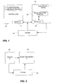
- the system of Fig. 1 includes an analog or power device 101 that is coupled to a control logic device 103.
- Device 101 is formed as an independent integrated circuit from device 103.
- Devices 101 and 103 may be provided as separate packaged ICs mounted on a printed circuit board or similar system integration.
- devices 101 and 103 may be integrated in chip form in the form of a multi-chip module.
- devices 101 and 103 may be provided on separate physical circuit boards or subsystems and coupled together by a communication link such as a wire, bus, or network as might occur in a line driver/receiver subsystem.
- Fig. 1 illustrates testing unit 105 which is not considered part of the system. Testing of electronic devices and systems occurs at multiple stages of manufacture including testing of partially processed wafers, wafer-level testing of chips, post-packaging test once chips are encapsulated, and system level test after the packaged devices are integrated into a system with other ICs.
- the present invention can be implemented using parametric information gathered at any one of these test operations, or using a combination of some or all of these test operations.
- Functional testing determines whether the device performs one or more specified functions (e.g., does a switch turn on and off), and is predominant in logic devices.
- Parametric testing determines whether the device exhibits characteristics that fall within specified range of allowable characteristics (e.g., do turn on time, input capacitance, on-resistance and the like meet specifications).
- Stress testing determines whether the device satisfies various performance criteria such as providing suitable safe operating area, latch-up current, and the like.
- testing involves applying a voltage or current stimulus to some set of device electrodes and monitoring response signals on other device electrodes.
- many device electrodes cannot be accessed after packaging, hence, testing that requires access to those electrodes cannot be performed at the system level.
- analog/power device 101 includes implementation-specific circuitry to such as amplifiers, power switches, and the like to drive current into a load such as a motor, flyback coil, antenna, fluorescent ballast circuit, magnetic read/write coil, or the like.
- An input/output (I/O) port such as serial I/O port 107 is provided for communicating with an external device (e.g., control logic device 103).
- Port 107 may be a serial or parallel communication port or both, and may comprise a multiple separate ports for coupling to various busses at the system level.
- the present invention contemplate leveraging an existing port that would already be provided on device 101 for some other purpose even if the digital signature feature of the present invention were not used.
- conventional motor driver circuits already include a two or three wire serial I/O interface for communicating with a control IC in operation. In this case, there would be no incremental cost in terms of chip size or complexity.
- a predetermined time such as power on
- Such an implementation might be appropriate, for example, if device 101 comprised a power transistor having only three leads and no explicit I/O port.
- the gate lead could be used to communicate the device signature, then revert to normal gate signal functionality after the predetermined time.
- the device signature could be communicated over existing device leads using frequency domain, time domain, or other multiplexing techniques.
- Device signature register 101 may comprise as few as two bits, or may comprise a tens or a few hundred bits. In an exemplary implementation it is expected that ten to fifty bits will allow ample storage space for device signature information.
- Device signature register 109 is coupled to I/O interface 107. This enables device signature register 109 to be programmed and potentially reprogrammed using information gathered by test unit 105.
- the value(s) stored in signature register 109 which preferably indicate device-specific parametric values, reside within the device itself either permanently or until overwritten.
- signature information that can be overwritten (i.e., dynamic signature information)
- the signature register 109 can be activated for write operations at power up by some other convenient trigger such as entering a self test mode.
- One or more critical parameters may be measured by integrated self test mechanisms. In this manner, a device signature can be modified dynamically well after the testing phase, and can provide information that allows performance to be optimized in the event of parametric changes or drift over time, or changes induced by changes in operating environment.
- the value stored in device signature register 109 is referred to as a device signature.
- the device signature value has a predefined format that is known to any device that later will access the device signature value, such as control logic device 103.
- the device signature value may be encoded or compressed.
- the device signature may indicate static or dynamic parameters as well as single valued parameters and dynamic parameters. For example, a single static value for on resistance may be included.
- parameters can be used to specify an equation or derating factor that in turn describes a dynamic parameter. For example, on resistance often changes as a function of current and a linear or quadratic equation could be developed to approximate this dynamic parameter.
- the encoded value could simply indicate a sort bin-type value. For example, the entire range of on resistances for a device could be subdivided into eight ranges, and the device signature could indicate (using only three bits), into which of the eight ranges that specific device fell.
- Metadata such as devices signature version number or the like.
- a manufacture may wish to change the device signature format over time while providing for backwards compatibility with existing devices.
- a few bits of information indicating the version is readily employed by devices that use the device signature to interpret, decode, decrypt, or otherwise use the parametric information contained therein.
- Control logic device 103 comprises, for example, an application specific integrated circuit (ASIC) having general-purpose, special-purpose, or programmable logic that performs control functions.
- control logic 103 may include hardware, firmware, or software processes that compute when to turn a disk drive actuator motor on and off to position a read write head in response to read/write commands from an external computer.
- Control logic device 103 implements an I/O interface 111 that is compatible with the I/O interface of analog/power device 101.
- control logic device 103 implements mechanisms and/or processes in hardware, firmware or software that obtain the device signature via I/O interfaces 111 and 107 from analog power device 109. Control logic device 103 also implements mechanisms and/or processes that respond to the device signature value to modify the behavior of the control logic. In this manner, control logic device 103 is able to automatically or semi-automatically fine-tune the system performance by modifying its behavior to more optimally interact with analog/power device 101.
- the control IC 103 when the system is first powered up the control IC 103 receives the device signature value.
- the device signature value may be transmitted only at initial power on, or may be retransmitted periodically or in response to a specific command from control logic 103.
- control device 103 modifies its behavior to, for example, shorten the time that device 101 is activated so that the intended motor behavior is achieved.
- the increase in precision enabled by the use of a device signature may simplify or eliminate the need for some feedback systems used to compensate for variances in current system design.
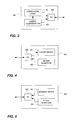
- Fig. 2 illustrates an alternative embodiment involving a sensor or monitor IC 201 and a signal processing IC 203.
- Sensor IC 201 includes a device signature register and I/O mechanism coupled so that the device signature register can be programmed to store a device signature value from a test apparatus 205.
- signal processing IC 203 obtains the device signature value, and modifies some hardware, firmware, or software defined behavior based on the device signature value.
- the device signature may indicate the full-scale output voltage span of the particular sensor device 201.
- Gain mechanisms or algorithms in signal processing IC 203 can be adapted automatically to provide a normalized full-scale span that is device-independent.
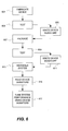
- Fig. 3 shows an exemplary control logic IC chip 300 in accordance with the present invention.
- operational logic 301 configured to perform designed data manipulation tasks, including memory, gate arrays, and data processing devices such as controller cores, arithmetic units and the like.
- Digital compensation logic 303 describes generally the devices and/or firmware and software processes that customize the behavior of the operational logic based upon the device signature. It is often practical to store a copy of the device signature in the digital compensation logic, although it is not mandatory to do so.
- I/O interface 305 provides a communication mechanism for obtaining the device signature and preferably for exchanging operational control data with an external driver IC 400 (shown in Fig. 4), monitor IC 500 (shown in Fig. 5) or the like.
- the exemplary driver IC 400 shown in Fig. 4 is akin to device 103 shown in Fig. 1 in that it includes a power driver device 401, device signature register 403, and an I/O interface 405.
- Driver device 401 typically occupies most of the chip area and may include, for example, one or more power switch(es), amplification circuitry, internal compensation circuitry and the like. Although most logic and control circuitry is implemented by external devices such as logic chip 300, it is contemplated that some logic may also be incorporated in driver device 401.
- Device signature register 403 may be implemented using any available memory cell technology but preferably uses non-volatile random access memory (RAM) or read only memory (ROM) technology that is compatible with the technology used to manufacture device driver 401 and I/O interface 405.
- I/O interface 405 implements, for example, a two-wile or three-wire serial interface, and typically includes one or more registers for holding values used by driver device 401 in operation. One or more of these registers may be allocated for implementing device signature
- Fig. 5 illustrates the principles of the present invention implemented in a system having an analog or linear input device having a device signature file.
- the exemplary sensor or monitor IC 500 shown in Fig. 5 includes a sensing device 501, device signature register 503, and an I/O interface 505.
- Sensing device 501 typically occupies most of the area of chip 501 and may include, for example, pressure sensor, chemical sensor, electromagnetic field sensor, optical sensor, or a combination of more than one type of sensor.
- Device 501 may include analog amplification circuitry and the like. It is contemplated that some logic may also be incorporated in sensor device 501, however, the present invention is particularly useful in applications where it is impractical to implement all necessary system logic on chip 501.
- Device signature register 503 may be implemented using any available memory cell technology but preferably uses non-volatile random access memory (RAM) or read only memory (ROM) technology that is compatible with the technology used to manufacture sensor device 501 and I/O interface 505.
- I/O interface 505 is largely analogous to interface 405 in construction, function and operation.
- Fig. 6 illustrates a flow diagram of various processes involved in a method of making and using a system in accordance with the present invention.
- Various operations and activities shown in the exemplary implementation of Fig. 6 may be omitted in particular applications.
- other processes, not shown will be integrated with the processes shown in Fig. 6 to satisfy needs of particular applications.
- the operations shown may be provided in alternative order while accomplishing the objectives set out herein.
- a device is fabricated using available processing techniques to include a signature file memory in accordance with the present invention. Because of the wide variety of technologies that can be used to implement memory cells, a device design can be augmented with an adequate amount of memory in most cases without materially impacting the design or operation of the chip.
- the device fabricated in 601 is tested to determine one or more performance parameters, and in 605 the parameters are stored directly or in encoded form in the signature file memory. It should be understood that operations 603/605 performed at wafer-level or die-level are optional, and that in many cases it is not practical or possible to perform parametric testing or writing to a signature file memory before packaging. However, in cases where steps 603/605 are practical, the signature file information can be used in later processing testing, and device sorting, and so may offer some downstream cost advantages.
- operation 607 the device is appropriately packaged using substantially conventional packaging techniques.
- operation 607 involves sawing wafers to separate devices, mounting the devices to a substrate or leadframe, and bonding wire or otherwise making electrical connections between the device and conductive leads that will extend from the packaged product.
- Operation 607 usually involves encapsulating the device in an appropriate manner with a polymer, metal can, or the like such that leads extend from the packaging.
- the packaged devices are tested in operation 609, at which point parametric testing can be performed in most cases.
- Testing 609 may also include various sorting algorithms.
- the parametric testing information is used to write to the device signature file as described above. To minimize pin count, it is preferred that some means of accessing the signature file through an existing lead is provided. This can be implemented using a variety of multiplexing mechanisms.
- the device includes a serial port that is configured by a control signal on an existing lead to access the signature file memory. In this manner, a signature file can be written by the same machine that is performing the testing as such machines are generally programmable to assert desired signals on desired pins.
- a multi-chip system is assembled using the product using appropriate assembly techniques such as printed circuit boards, multi-chip modules and the like.
- a device having a signature file is coupled to a logic device that is capable of reading the signature file in 615 and adapting some feature of the system behavior to the value stored in the signature file.
- the multiplexing mechanism used to write data to the device signature tile is used to read data from the device signature file, although other equivalent access mechanisms are contemplated and may be appropriate in certain circumstances.
- the system self tunes using the value stored in the device signature file.
- the tuning in operation 617 may account for multiple signature files in systems with multiple chips.
- tuning involves either using an algorithm to compute a compensation factor that accounts for the particular device performance indicated by the device signature or using the device signature to access a look-up table of stored compensation factors. For example, gain of an amplifier may be adjusted to affect input/output impedance matching or to match a driver more accurately to a driven load. In the past, such fine-tuning was performed manually, if at all. Even if manual tuning is used in conjunction with the present invention, the signature file will lessen or eliminate need for complex in-circuit parametric testing during the tuning process.
Landscapes
- Engineering & Computer Science (AREA)
- Power Engineering (AREA)
- Semiconductor Integrated Circuits (AREA)
- Tests Of Electronic Circuits (AREA)
- Logic Circuits (AREA)
Abstract
Description
Claims (18)
- A multi chip system comprising:a first integrated circuit (IC) device; anda companion IC coupled to the first IC to lonn a system, wherein the first IC includes a performance parameter encoded thereon.
- The system of claim 1 wherein the performance parameter can be obtained the companion IC and used to fine tune the companion chip to the specific parameters of the at first IC.
- The system of claim 1 or 2 wherein the companion chip automatically or semi-automatically fine tunes using the performance parameter.
- The system of any of claims 1 to 3 wherein the first IC comprises linear circuitry and/or a motor driver and the companion chip comprises digital logic and/or control logic.
- The system of any preceding claim further comprising a plurality of companion ICs coupled to the first IC, wherein each of the plurality of companion ICs are configured to obtain the at least one performance parameter.
- The system of any preceding claim further comprising mechanisms in the first IC and the companion IC for exchanging the at least one performance parameter upon power up.
- An integrated circuit comprising:operational devices configured to perform a specific function; anda register for storing a value, called a device signature, indicating at least one performance parameter associated with the operational devices.
- The integrated circuit of claim 7 further comprising a mechanism for communicating the device signature with at least one external companion chip after the integrated circuit is incorporated in a system.
- The integrated circuit of claim 8 wherein the mechanism for communicating comprises a two-wire serial interface.
- The integrated circuit of any of claims 7 to 9 wherein the register comprises non-volatile memory.
- The integrated circuit of any of claims 7 to 10 wherein the operational devices comprise a motor driver circuit and/or a sensor.
- The integrated circuit of any of claims 7 to 11 wherein the register comprises less than 50 bits of storage.
- A companion integrated circuit (IC) for a multi-chip system, the companion IC comprising:an input/output mechanism for reading a device signature from an external device.
- The IC of claim 13 wherein the device signature comprises a value indicating at least one performance parameter of the external device.
- The IC of claim 13 or 14 further comprising a mechanism for modifying its own behavior based on the device signature obtained after the IC is incorporated in a system.
- A method of making a multi-chip electronic system comprising the acts of:fabricating a first integrated circuit (IC);testing the first integrated circuit to determine at least one parameter indicating a performance characteristic of the first integrated circuit; andstoring a value corresponding to the parameter on the first integrated circuit.
- The method of claim 16 further comprising incorporating the integrated circuit into a system comprising a second integrated circuit; and
exchanging the stored value between the first integrated circuit to the second integrated circuit. - The method of claim 17 further comprising tuning behavior of the second integrated circuit in response to exchanging the stored value.
Applications Claiming Priority (2)
| Application Number | Priority Date | Filing Date | Title |
|---|---|---|---|
| US164079 | 2002-06-05 | ||
| US10/164,079 US7844747B2 (en) | 2002-06-05 | 2002-06-05 | Performance tuning using encoded performance parameter information |
Publications (2)
| Publication Number | Publication Date |
|---|---|
| EP1376357A2 true EP1376357A2 (en) | 2004-01-02 |
| EP1376357A3 EP1376357A3 (en) | 2004-01-07 |
Family
ID=29710127
Family Applications (1)
| Application Number | Title | Priority Date | Filing Date |
|---|---|---|---|
| EP03253398A Withdrawn EP1376357A3 (en) | 2002-06-05 | 2003-05-30 | Integrated circuit having internal signature |
Country Status (3)
| Country | Link |
|---|---|
| US (2) | US7844747B2 (en) |
| EP (1) | EP1376357A3 (en) |
| JP (1) | JP2004012463A (en) |
Families Citing this family (7)
| Publication number | Priority date | Publication date | Assignee | Title |
|---|---|---|---|---|
| US6996786B2 (en) * | 2003-09-30 | 2006-02-07 | International Business Machines Corporation | Latch-up analysis and parameter modification |
| DE102005007333B4 (en) * | 2004-05-07 | 2008-07-03 | Avago Technologies General Ip (Singapore) Pte. Ltd. | Multi-chip packages with high-speed serial communications between semiconductor dies |
| US7342310B2 (en) * | 2004-05-07 | 2008-03-11 | Avago Technologies General Ip Pte Ltd | Multi-chip package with high-speed serial communications between semiconductor die |
| US8212655B2 (en) * | 2006-03-30 | 2012-07-03 | Rosemount Inc. | System and method for identification of process components |
| US8159241B1 (en) * | 2007-04-24 | 2012-04-17 | Marvell International Ltd. | Method and apparatus for on-chip adjustment of chip characteristics |
| US8990744B2 (en) | 2013-04-16 | 2015-03-24 | Infineon Technologies Ag | Electrical measurement based circuit wiring layout modification method and system |
| US10504353B2 (en) | 2015-07-27 | 2019-12-10 | Hill-Rom Services, Inc. | Customized bed exit warnings to modify patient behavior |
Family Cites Families (31)
| Publication number | Priority date | Publication date | Assignee | Title |
|---|---|---|---|---|
| US4150331A (en) * | 1977-07-29 | 1979-04-17 | Burroughs Corporation | Signature encoding for integrated circuits |
| US4769883A (en) * | 1983-03-07 | 1988-09-13 | Westinghouse Electric Corp. | Method for tuning a microwave integrated circuit |
| JPS6072067A (en) * | 1983-09-28 | 1985-04-24 | Kyodo Printing Co Ltd | Collating method of id card owner |
| US4906956A (en) * | 1987-10-05 | 1990-03-06 | Menlo Industries, Inc. | On-chip tuning for integrated circuit using heat responsive element |
| US5122970A (en) * | 1988-06-17 | 1992-06-16 | Hewlett-Packard Company | Improved sensor |
| EP0693212B1 (en) * | 1993-04-07 | 1999-12-08 | Noise Cancellation Technologies, Inc. | Hybrid analog/digital vibration control system |
| US5729158A (en) * | 1995-07-07 | 1998-03-17 | Sun Microsystems, Inc. | Parametric tuning of an integrated circuit after fabrication |
| US5619453A (en) * | 1995-07-28 | 1997-04-08 | Micron Quantum Devices, Inc. | Memory system having programmable flow control register |
| JP3175603B2 (en) | 1996-09-20 | 2001-06-11 | 日本電気株式会社 | Semiconductor integrated circuit device |
| US5873063A (en) * | 1997-05-16 | 1999-02-16 | United Microelectronics Corporation | LSP speech synthesis device |
| US5764655A (en) * | 1997-07-02 | 1998-06-09 | International Business Machines Corporation | Built in self test with memory |
| US6087190A (en) * | 1997-10-08 | 2000-07-11 | Macronix International Co., Ltd. | Automatic test process with non-volatile result table store |
| US6229378B1 (en) * | 1997-12-31 | 2001-05-08 | Intel Corporation | Using programmable jumpers to set an IC device's bit-encoded output during manufacturing and testing |
| US6111509A (en) * | 1998-02-26 | 2000-08-29 | Bed-Check Corporation | Microprocessor based bed patient monitor |
| AU3841999A (en) * | 1998-06-05 | 1999-12-30 | Landis & Gyr Communications Sarl | Preloaded ic-card and method for authenticating the same |
| US6185712B1 (en) * | 1998-07-02 | 2001-02-06 | International Business Machines Corporation | Chip performance optimization with self programmed built in self test |
| US6574679B1 (en) * | 1999-07-26 | 2003-06-03 | International Business Machines Corporation | Method and apparatus for identifying hardware |
| US6671765B1 (en) * | 1999-11-22 | 2003-12-30 | Texas Instruments Incorporated | Architecture enabling code overlay using a dedicated endpoint |
| US7363422B2 (en) * | 2000-01-05 | 2008-04-22 | Rambus Inc. | Configurable width buffered module |
| US6625785B2 (en) * | 2000-04-19 | 2003-09-23 | Georgia Tech Research Corporation | Method for diagnosing process parameter variations from measurements in analog circuits |
| US6873044B2 (en) * | 2000-09-11 | 2005-03-29 | Xytrans, Inc. | Microwave monolithic integrated circuit package |
| US6630860B1 (en) * | 2000-09-20 | 2003-10-07 | Applied Micro Circuits Corporation | Programmable phase locked-loop filter architecture for a range selectable bandwidth |
| US6856849B2 (en) * | 2000-12-06 | 2005-02-15 | Advanced Micro Devices, Inc. | Method for adjusting rapid thermal processing (RTP) recipe setpoints based on wafer electrical test (WET) parameters |
| US6885853B2 (en) * | 2001-04-11 | 2005-04-26 | National Scientific Corporation | Communications receiver with integrated IF filter and method therefor |
| US6590441B2 (en) * | 2001-06-01 | 2003-07-08 | Qualcomm Incorporated | System and method for tuning a VLSI circuit |
| US6556345B1 (en) * | 2001-06-21 | 2003-04-29 | Onetta, Inc. | Optical network equipment with control and data paths |
| JP3588599B2 (en) * | 2001-07-05 | 2004-11-10 | 株式会社東芝 | Semiconductor buffer capacity adjustment method, semiconductor buffer capacity adjustment system, and semiconductor device |
| US6614689B2 (en) * | 2001-08-13 | 2003-09-02 | Micron Technology, Inc. | Non-volatile memory having a control mini-array |
| US6583642B2 (en) * | 2001-08-17 | 2003-06-24 | Silicon Integrated Systems Corp. | Apparatus and method for automatic determination of operating frequency with built-in self-test |
| US6721924B2 (en) * | 2001-09-28 | 2004-04-13 | Intel Corporation | Noise and power optimization in high performance circuits |
| US6851018B2 (en) * | 2002-03-27 | 2005-02-01 | Hewlett-Packard Development Company, L.P. | Exchanging operation parameters between a data storage device and a controller |
-
2002
- 2002-06-05 US US10/164,079 patent/US7844747B2/en not_active Expired - Fee Related
-
2003
- 2003-05-30 EP EP03253398A patent/EP1376357A3/en not_active Withdrawn
- 2003-06-05 JP JP2003161170A patent/JP2004012463A/en active Pending
-
2010
- 2010-10-20 US US12/908,661 patent/US20110032036A1/en not_active Abandoned
Also Published As
| Publication number | Publication date |
|---|---|
| US7844747B2 (en) | 2010-11-30 |
| EP1376357A3 (en) | 2004-01-07 |
| US20110032036A1 (en) | 2011-02-10 |
| JP2004012463A (en) | 2004-01-15 |
| US20030229730A1 (en) | 2003-12-11 |
Similar Documents
| Publication | Publication Date | Title |
|---|---|---|
| US20110032036A1 (en) | Performance tuning using encoded performance parameter information | |
| US7269043B2 (en) | Memory module and impedance calibration method of semiconductor memory device | |
| KR100319286B1 (en) | Semiconductor circuit for electronic unit | |
| EP1324554A2 (en) | Bi-directional buffer with impedance matching | |
| US7808269B2 (en) | Semiconductor integrated circuit | |
| US11749325B2 (en) | Memory device having an enhanced ESD protection and a secure access from a testing machine | |
| US20030016574A1 (en) | Method of adjusting semiconductor buffer capability of semiconductor device, electronic system, and semiconductor device | |
| US20030057986A1 (en) | Integrated on-chip process, temperature, and voltage sensor module | |
| CN103746683B (en) | Systems and methods for using integrated circuit pins as current-limited inputs and open-drain outputs | |
| US20090076747A1 (en) | Test board and test system | |
| US11430535B2 (en) | Semiconductor device and test method thereof | |
| CN102045054B (en) | Method and related device for correcting output/input circuit | |
| US7315185B2 (en) | Low voltage differential signal receiver and methods of calibrating a termination resistance of a low voltage differential signal receiver | |
| US20020149984A1 (en) | Semiconductor physical quantity sensing device | |
| US9236867B2 (en) | Apparatus for mixed signal interface circuitry and associated methods | |
| US20040027872A1 (en) | Semiconductor physical quantity sensing device | |
| CN120949142A (en) | Multi-range calibration for single-pin parameter measurement units | |
| US20070192050A1 (en) | Interface control apparatus and setting method for an interface | |
| US8039274B2 (en) | Multi-chip package semiconductor device and method of detecting a failure thereof | |
| KR20050087301A (en) | Socket managing system and test system having the socket managing system | |
| KR20070088845A (en) | Impedance calibration method of memory module and semiconductor devices included in memory module | |
| CN114325532B (en) | Pin driver and test equipment calibration | |
| CN114678058B (en) | Calibration circuit of MRAM read-write voltage, calibration method thereof and MRAM | |
| US20130111223A1 (en) | Electronic device and method for driving an internal function block of a processor of the electronic device to operate in a linear region | |
| CN114492286B (en) | Method and device for controlling chip |
Legal Events
| Date | Code | Title | Description |
|---|---|---|---|
| PUAI | Public reference made under article 153(3) epc to a published international application that has entered the european phase |
Free format text: ORIGINAL CODE: 0009012 |
|
| PUAL | Search report despatched |
Free format text: ORIGINAL CODE: 0009013 |
|
| AK | Designated contracting states |
Kind code of ref document: A2 Designated state(s): AT BE BG CH CY CZ DE DK EE ES FI FR GB GR HU IE IT LI LU MC NL PT RO SE SI SK TR |
|
| AX | Request for extension of the european patent |
Extension state: AL LT LV MK |
|
| AK | Designated contracting states |
Kind code of ref document: A3 Designated state(s): AT BE BG CH CY CZ DE DK EE ES FI FR GB GR HU IE IT LI LU MC NL PT RO SE SI SK TR |
|
| AX | Request for extension of the european patent |
Extension state: AL LT LV MK |
|
| 17P | Request for examination filed |
Effective date: 20040702 |
|
| AKX | Designation fees paid |
Designated state(s): DE FR GB IT |
|
| 17Q | First examination report despatched |
Effective date: 20070402 |
|
| STAA | Information on the status of an ep patent application or granted ep patent |
Free format text: STATUS: THE APPLICATION IS DEEMED TO BE WITHDRAWN |
|
| 18D | Application deemed to be withdrawn |
Effective date: 20091201 |