EP1376238A2 - A system for correcting aberration and distortion in EUV litography - Google Patents
A system for correcting aberration and distortion in EUV litography Download PDFInfo
- Publication number
- EP1376238A2 EP1376238A2 EP03013978A EP03013978A EP1376238A2 EP 1376238 A2 EP1376238 A2 EP 1376238A2 EP 03013978 A EP03013978 A EP 03013978A EP 03013978 A EP03013978 A EP 03013978A EP 1376238 A2 EP1376238 A2 EP 1376238A2
- Authority
- EP
- European Patent Office
- Prior art keywords
- reticle
- wafer
- deformable
- chuck
- distortion
- Prior art date
- Legal status (The legal status is an assumption and is not a legal conclusion. Google has not performed a legal analysis and makes no representation as to the accuracy of the status listed.)
- Withdrawn
Links
Images




Classifications
-
- G—PHYSICS
- G03—PHOTOGRAPHY; CINEMATOGRAPHY; ANALOGOUS TECHNIQUES USING WAVES OTHER THAN OPTICAL WAVES; ELECTROGRAPHY; HOLOGRAPHY
- G03F—PHOTOMECHANICAL PRODUCTION OF TEXTURED OR PATTERNED SURFACES, e.g. FOR PRINTING, FOR PROCESSING OF SEMICONDUCTOR DEVICES; MATERIALS THEREFOR; ORIGINALS THEREFOR; APPARATUS SPECIALLY ADAPTED THEREFOR
- G03F7/00—Photomechanical, e.g. photolithographic, production of textured or patterned surfaces, e.g. printing surfaces; Materials therefor, e.g. comprising photoresists; Apparatus specially adapted therefor
- G03F7/70—Microphotolithographic exposure; Apparatus therefor
- G03F7/70216—Mask projection systems
- G03F7/70233—Optical aspects of catoptric systems, i.e. comprising only reflective elements, e.g. extreme ultraviolet [EUV] projection systems
-
- G—PHYSICS
- G03—PHOTOGRAPHY; CINEMATOGRAPHY; ANALOGOUS TECHNIQUES USING WAVES OTHER THAN OPTICAL WAVES; ELECTROGRAPHY; HOLOGRAPHY
- G03F—PHOTOMECHANICAL PRODUCTION OF TEXTURED OR PATTERNED SURFACES, e.g. FOR PRINTING, FOR PROCESSING OF SEMICONDUCTOR DEVICES; MATERIALS THEREFOR; ORIGINALS THEREFOR; APPARATUS SPECIALLY ADAPTED THEREFOR
- G03F7/00—Photomechanical, e.g. photolithographic, production of textured or patterned surfaces, e.g. printing surfaces; Materials therefor, e.g. comprising photoresists; Apparatus specially adapted therefor
- G03F7/70—Microphotolithographic exposure; Apparatus therefor
- G03F7/70216—Mask projection systems
- G03F7/70258—Projection system adjustments, e.g. adjustments during exposure or alignment during assembly of projection system
-
- G—PHYSICS
- G03—PHOTOGRAPHY; CINEMATOGRAPHY; ANALOGOUS TECHNIQUES USING WAVES OTHER THAN OPTICAL WAVES; ELECTROGRAPHY; HOLOGRAPHY
- G03F—PHOTOMECHANICAL PRODUCTION OF TEXTURED OR PATTERNED SURFACES, e.g. FOR PRINTING, FOR PROCESSING OF SEMICONDUCTOR DEVICES; MATERIALS THEREFOR; ORIGINALS THEREFOR; APPARATUS SPECIALLY ADAPTED THEREFOR
- G03F7/00—Photomechanical, e.g. photolithographic, production of textured or patterned surfaces, e.g. printing surfaces; Materials therefor, e.g. comprising photoresists; Apparatus specially adapted therefor
- G03F7/70—Microphotolithographic exposure; Apparatus therefor
- G03F7/70216—Mask projection systems
- G03F7/70258—Projection system adjustments, e.g. adjustments during exposure or alignment during assembly of projection system
- G03F7/70266—Adaptive optics, e.g. deformable optical elements for wavefront control, e.g. for aberration adjustment or correction
-
- G—PHYSICS
- G03—PHOTOGRAPHY; CINEMATOGRAPHY; ANALOGOUS TECHNIQUES USING WAVES OTHER THAN OPTICAL WAVES; ELECTROGRAPHY; HOLOGRAPHY
- G03F—PHOTOMECHANICAL PRODUCTION OF TEXTURED OR PATTERNED SURFACES, e.g. FOR PRINTING, FOR PROCESSING OF SEMICONDUCTOR DEVICES; MATERIALS THEREFOR; ORIGINALS THEREFOR; APPARATUS SPECIALLY ADAPTED THEREFOR
- G03F7/00—Photomechanical, e.g. photolithographic, production of textured or patterned surfaces, e.g. printing surfaces; Materials therefor, e.g. comprising photoresists; Apparatus specially adapted therefor
- G03F7/70—Microphotolithographic exposure; Apparatus therefor
- G03F7/70216—Mask projection systems
- G03F7/703—Non-planar pattern areas or non-planar masks, e.g. curved masks or substrates
-
- G—PHYSICS
- G03—PHOTOGRAPHY; CINEMATOGRAPHY; ANALOGOUS TECHNIQUES USING WAVES OTHER THAN OPTICAL WAVES; ELECTROGRAPHY; HOLOGRAPHY
- G03F—PHOTOMECHANICAL PRODUCTION OF TEXTURED OR PATTERNED SURFACES, e.g. FOR PRINTING, FOR PROCESSING OF SEMICONDUCTOR DEVICES; MATERIALS THEREFOR; ORIGINALS THEREFOR; APPARATUS SPECIALLY ADAPTED THEREFOR
- G03F7/00—Photomechanical, e.g. photolithographic, production of textured or patterned surfaces, e.g. printing surfaces; Materials therefor, e.g. comprising photoresists; Apparatus specially adapted therefor
- G03F7/70—Microphotolithographic exposure; Apparatus therefor
- G03F7/70691—Handling of masks or workpieces
- G03F7/707—Chucks, e.g. chucking or un-chucking operations or structural details
-
- G—PHYSICS
- G03—PHOTOGRAPHY; CINEMATOGRAPHY; ANALOGOUS TECHNIQUES USING WAVES OTHER THAN OPTICAL WAVES; ELECTROGRAPHY; HOLOGRAPHY
- G03F—PHOTOMECHANICAL PRODUCTION OF TEXTURED OR PATTERNED SURFACES, e.g. FOR PRINTING, FOR PROCESSING OF SEMICONDUCTOR DEVICES; MATERIALS THEREFOR; ORIGINALS THEREFOR; APPARATUS SPECIALLY ADAPTED THEREFOR
- G03F7/00—Photomechanical, e.g. photolithographic, production of textured or patterned surfaces, e.g. printing surfaces; Materials therefor, e.g. comprising photoresists; Apparatus specially adapted therefor
- G03F7/70—Microphotolithographic exposure; Apparatus therefor
- G03F7/70691—Handling of masks or workpieces
- G03F7/707—Chucks, e.g. chucking or un-chucking operations or structural details
- G03F7/70708—Chucks, e.g. chucking or un-chucking operations or structural details being electrostatic; Electrostatically deformable vacuum chucks
-
- G—PHYSICS
- G03—PHOTOGRAPHY; CINEMATOGRAPHY; ANALOGOUS TECHNIQUES USING WAVES OTHER THAN OPTICAL WAVES; ELECTROGRAPHY; HOLOGRAPHY
- G03F—PHOTOMECHANICAL PRODUCTION OF TEXTURED OR PATTERNED SURFACES, e.g. FOR PRINTING, FOR PROCESSING OF SEMICONDUCTOR DEVICES; MATERIALS THEREFOR; ORIGINALS THEREFOR; APPARATUS SPECIALLY ADAPTED THEREFOR
- G03F7/00—Photomechanical, e.g. photolithographic, production of textured or patterned surfaces, e.g. printing surfaces; Materials therefor, e.g. comprising photoresists; Apparatus specially adapted therefor
- G03F7/70—Microphotolithographic exposure; Apparatus therefor
- G03F7/70691—Handling of masks or workpieces
- G03F7/70783—Handling stress or warp of chucks, masks or workpieces, e.g. to compensate for imaging errors or considerations related to warpage of masks or workpieces due to their own weight
-
- G—PHYSICS
- G03—PHOTOGRAPHY; CINEMATOGRAPHY; ANALOGOUS TECHNIQUES USING WAVES OTHER THAN OPTICAL WAVES; ELECTROGRAPHY; HOLOGRAPHY
- G03F—PHOTOMECHANICAL PRODUCTION OF TEXTURED OR PATTERNED SURFACES, e.g. FOR PRINTING, FOR PROCESSING OF SEMICONDUCTOR DEVICES; MATERIALS THEREFOR; ORIGINALS THEREFOR; APPARATUS SPECIALLY ADAPTED THEREFOR
- G03F7/00—Photomechanical, e.g. photolithographic, production of textured or patterned surfaces, e.g. printing surfaces; Materials therefor, e.g. comprising photoresists; Apparatus specially adapted therefor
- G03F7/70—Microphotolithographic exposure; Apparatus therefor
- G03F7/708—Construction of apparatus, e.g. environment aspects, hygiene aspects or materials
- G03F7/70858—Environment aspects, e.g. pressure of beam-path gas, temperature
- G03F7/70866—Environment aspects, e.g. pressure of beam-path gas, temperature of mask or workpiece
- G03F7/70875—Temperature, e.g. temperature control of masks or workpieces via control of stage temperature
-
- G—PHYSICS
- G03—PHOTOGRAPHY; CINEMATOGRAPHY; ANALOGOUS TECHNIQUES USING WAVES OTHER THAN OPTICAL WAVES; ELECTROGRAPHY; HOLOGRAPHY
- G03F—PHOTOMECHANICAL PRODUCTION OF TEXTURED OR PATTERNED SURFACES, e.g. FOR PRINTING, FOR PROCESSING OF SEMICONDUCTOR DEVICES; MATERIALS THEREFOR; ORIGINALS THEREFOR; APPARATUS SPECIALLY ADAPTED THEREFOR
- G03F7/00—Photomechanical, e.g. photolithographic, production of textured or patterned surfaces, e.g. printing surfaces; Materials therefor, e.g. comprising photoresists; Apparatus specially adapted therefor
- G03F7/70—Microphotolithographic exposure; Apparatus therefor
- G03F7/708—Construction of apparatus, e.g. environment aspects, hygiene aspects or materials
- G03F7/70858—Environment aspects, e.g. pressure of beam-path gas, temperature
- G03F7/70883—Environment aspects, e.g. pressure of beam-path gas, temperature of optical system
- G03F7/70891—Temperature
-
- Y—GENERAL TAGGING OF NEW TECHNOLOGICAL DEVELOPMENTS; GENERAL TAGGING OF CROSS-SECTIONAL TECHNOLOGIES SPANNING OVER SEVERAL SECTIONS OF THE IPC; TECHNICAL SUBJECTS COVERED BY FORMER USPC CROSS-REFERENCE ART COLLECTIONS [XRACs] AND DIGESTS
- Y10—TECHNICAL SUBJECTS COVERED BY FORMER USPC
- Y10T—TECHNICAL SUBJECTS COVERED BY FORMER US CLASSIFICATION
- Y10T428/00—Stock material or miscellaneous articles
- Y10T428/24—Structurally defined web or sheet [e.g., overall dimension, etc.]
- Y10T428/24802—Discontinuous or differential coating, impregnation or bond [e.g., artwork, printing, retouched photograph, etc.]
Definitions
- This invention is in the technical field of extreme ultraviolet (EUV) lithography.
- the reticle In EUV lithography, the reticle is reflective and is chucked in the lithography tool by its unpatterned surface, not around its periphery as required for a reticle of a transmissive type. Because the reticle is reflective, it is illuminated away from normal incidence. Consequently, any variation in height of the reticle-patterned surface will lead to displacement of features, or distortion, at the wafer. If either the back side of the reticle or the mating chuck surface is not flat, or if particles are trapped therebetween during chucking, furthermore, the front surface of the reticle will become distorted, leading to further feature displacement at the wafer.
- the reticle-patterned surface is composed of a multi-layer film coating, and the reflectivity of the coating is unlikely to be much greater than 0.65.
- the reticle will absorb a significant amount of EUV, power, and therefore must be actively cooled.
- the coating has a tensile stress, the reticle may be slightly bowed and must be flattened by the chuck.
- high throughput EUV lithography tools are calling for reticle stage accelerations of up to 8g (g being the gravitational acceleration). The reticle must therefore be held very firmly to avoid slippage and possible deformation caused by the acceleration.
- a system For correcting aberration and distortion in EUV lithography, a system according to this invention places a reticle on a deformable reticle chuck, and a reticle height sensor is used to measure the surface height of the reticle placed on the deformable reticle chuck.
- An illumination system projects EUV radiation onto the reticle placed on said reticle chuck and collects and projects reflected EUV radiation from the reticle through the optical system's projection optics onto a wafer placed on a wafer chuck.
- a deformable mirror is preferably disposed proximal to the exit pupil of the projection optics as the last of a plurality of reflectors of the optical system. The deformable reticle chuck and the deformable mirror are controlled such that aberration and distortion of an image of the reticle formed on the wafer by the optical system are corrected based on the height measured by the reticle height sensor.
- the deformable reticle chuck according to this invention to be used in such a system may be characterized as comprising a supporting structure, a deformable membrane disposed above the supporting structure and being comprised of a dielectric layer of a dielectric material and a conductive layer of an electrically conductive material, a voltage source such as a battery connected to a conductive coating on the back side of the reticle and to the conductive layer to generate an electrostatic attractive force between them, a plurality of actuator rods each connected through a weak spring to a corresponding one of actuators.
- the actuator rods penetrate the supporting structure and protrude above the top surface of the supporting structure and support and attach to the membrane.
- a chamber formed between the membrane and the top surface of the supporting structure contains a heat-conducting gas such as helium.
- the supporting structure has throughholes through which a coolant fluid is passed, and the deformable reticle chuck may further comprise a clamping plate for clamping the actuator rods in place after they are adjusted.
- the system may further comprise a wafer height sensor that detects the height of the wafer such that aberration and distortion of the image are corrected based also on the height measured by the wafer height sensor.
- the wafer chuck may be made deformable such that distortion of the image is corrected also by deforming the wafer chuck.
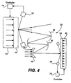
- Fig. 4 shows schematically an EUV lithographic projection apparatus incorporating an aberration and distortion correcting system of this invention.
- EUV radiation from a source (not shown) is made incident on a reticle 15 set on a deformable reticle chuck 10, and reflected radiation from the reticle 15 is focused on a wafer 25 set on a deformable wafer chuck 20 by means of an optical system 30 including a plurality of intermediate reflectors 35 and a deformable mirror 40 serving as the last-stage reflector located proximally to the exit pupil (not shown) of the optical system 30.
- Numerals 16 and 26 respectively indicate a reticle height sensor and a wafer height sensor.
- Controller 18 processes the information from reticle height sensor 16 and adjusts the deformable reticle chuck 10.
- Controller 28 plays a similar role for the wafer height sensor 26 and deformable wafer chuck 20.
- the aberrated wave front has a characteristic shape over the exit pupil.
- the wave fronts of the various aberrations can be characterized by Zernike polynomials which depend only on the radius r from the center of the pupil and the azimuthal angle ⁇ .
- Wavefront shapes which cause distortion have a linear dependence on r, but many other aberrations also include a linear dependence on r, and hence any errors in measuring or adjusting the mirror surface to cancel other aberrations may inadvertently create distortion.
- the change in optical path is given by 2z/cos ⁇ (since EUV lithography is done in vacuum, the index of refraction is 1.0). This corresponds to the local shift in the aberrated wave front, so for angles of incidence not too big, the aberrated wave front changes by twice the local displacement of the mirror surface. Since the aberrated wave front is not expected to differ from that of a spherical wave by more than approximately 1nm, it follows that control of the mirror must be very precise, since the mirror surface must be controlled to better than 0.5 nm.
- the EUV lithography tool is a stepper
- the appropriate reticle shape can be determined and set, and no further changes are needed.
- the wafer and reticle are mechanically scanned synchronously such that an arc shaped stripe of illumination moves across the reticle and wafer.
- This stripe represents the entire field of the projection optics.
- the wafer it is typically a few mm wide in the direction of the scan and the width of the chip in length, say, of 25 - 33 mm.
- the stripe dimensions might be about 5 - 10 mm by over 100 mm.
- the reticle would have to be deformed within a region of less than 10 mm in length. Given the thickness of the reticle 6.35 mm and the density of actuators needed to deform the reticle within a space of about 10 mm, this may be quite difficult to achieve. Also, the deformation must be applied dynamically to the reticle as it scans through the projection optics field; i.e. any deformation in the reticle must "follow" the illumination stripe across the reticle surface. Thus, correction of distortion originating in the projection optics along the scan direction may be very limited in practice.
- Figs. 5 and 6 are referenced next to explain the structure of the deformable reticle chuck 10 according to an embodiment of this invention.
- the chuck and reticle are described in the conventional orientation, with the reticle sitting on top of the chuck.
- the chuck may be upside down with the reticle attached beneath it.
- the deformable reticle chuck 10 is an electrostatic chuck.
- the surface of the unpattemed side of the reticle 15 is coated with an electrically conductive material such as a metallic film.
- the main body portion of the reticle 15 made of a glass or ceramic material is indicated by numeral 151 and its coating of the conductive material is indicated by numeral 152.
- a double-layered thin membrane comprised of a dielectric layer 51 and an electrically conductive layer 52 below the dielectric layer 51.
- a power supply or battery 53 serving as a voltage source connected to both the conductive coating 152 on the reticle 15 and to the conductive layer 52 at the top of the chuck 10 supplies an attractive electrostatic force therebetween across the dielectric layer 51, the latter serving to prevent the two conductive layers 52 and 152 from shorting.
- the thin membrane of the dielectric and conductive layers 51 and 52 is attached to actuator rods 60 attached to actuators (not shown) distributed through the surface area of the chuck 10 and each adapted to move up and down, penetrating the supporting structure 50 by the actuating force of a corresponding one of the actuators.
- the actuator rods 60 are restricted to the region 70 of the reticle 15 which is imaged to the wafer.
- a cooling gas such as helium at sub-atmospheric pressure is contained in a thin chamber 56 beneath the membrane and transports heat by conduction from the reticle 15 through the membrane to the supporting structure 50 which is provided with througbholes 55 for a coolant to flow through.
- the membrane is secured to the supporting structure 50 along a rim 76 at its periphery 75, providing a hermetic seal.
- Displacement actuators control the shape of the reticle by adjusting their length between the reticle and a fixed base plate.
- any distortion of the base plate will change the reticle figure unless the displacement of the actuator caused by the distortion of the base plate is corrected.
- a force actuator applies a specified force to the reticle to achieve the desired deformation.
- displacement actuators may be difficult to adjust to obtain very small length changes and are not generally well-suited to the types of adjustment required for lithographic applications, particularly in terms of stability.
- a relatively weak spring between the fixed end of an actuator e.g.
- reticle deformation may be accomplished with force actuators or displacement actuators with much improved stability and control characteristics by the addition of a weak spring in the mechanical linkage such that they function in the manner of a stable and easily controllable force actuator.
- weak springs 65 are inserted between the actuators and the actuator rods 60.
- the quantity ⁇ z m is typically of the order of a nanometer or less, and it is not easy to control displacements that small. But by adjusting the spring constant k s so that ⁇ z s is much larger than a nanometer, control of the reticle displacement is simplified, and many different actuator types may be used. This condition is ensured by making k s sufficiently small relative to K m . This is the meaning of a weak spring.
- the thermal conductivity k of a gas is essentially independent of pressure as long as the mean free path of the gas molecules is small compared to the system dimensions. This is discussed in more detail below. This fact allows using a gas at a relatively low pressure in the chuck with little effect on the heat transfer. The relatively low pressure avoids distorting the membrane of the chuck. A large deformation would reduce the area of contact between the distorted membrane and the flat reticle, and it might weaken the membrane. It might also distort the reticle.
- the membrane with the dielectric layer 51 and the conductive layer 52 contacts the reticle 15 at all points on its backside such that the attractive electrostatic force is maximal and slippage during acceleration will be minimized. Since this membrane is deformable, it can accommodate reticles with non-flat backsides or trapped particles without inducing unwanted deformation of the front surface.
- the actuators (not shown) associated with the actuator rods 60 are controlled by the controller 18 using signals from the reticle height sensor 16, which monitors the reticle surface, so as to deform the backside of the reticle 15 appropriately such that the front surface of the reticle 15 will have a proper height and shape. Thus, image distortion at the wafer 25 due to non-telecentricity can be reduced.
- the actuators apply a specified force to the back of the reticle 15 through the actuator rods 60. Since the reticle is typically changed infrequently, the actuator rods 60 may be clamped in place (say, by means of a clamping plate shown at 62 in Fig. 6) after adjustment, and the actuator power can be turned off for stability and minimum heat generation.
- the clamp plate 62 is located below the springs 65, so the reticle remains positioned by means of force actuation, not displacement actuation.
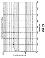
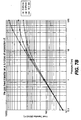
- FIG. 7A is based on expressions from the paper "Low temperature etch chuck: modeling and experimental results of heat transfer and wafer temperature," by D. Wright et al., published in Journal of Vacuum Science and Technology, A10, 1065 (1992).
- the heat transfer coefficient decreases by only about 15% as the pressure decreases from an atmospheric pressure of 760 Torr to about 50 Torr, which is about 6% of atmospheric pressure.
- the mean free path in He at a temperature of 25 °C. is about 2.9 ⁇ m, which is a small fraction of the separation d.
- FIG. 7B shows the heat transfer of He for several values of d.
- a small value of d enhances the heat transfer.
- the heat transfer is about 1305 W/m 2 -°K, which is about 8% less than its value at atmospheric pressure.
- the deformable reticle chuck 10 thus structured is vacuum-compatible.
- the EUV reticle is in a vacuum environment.
- the stroke required for the actuators is relatively small but a few of the actuators may be adapted for longer strokes for use when the reticle 15 is popped up off the chuck 10 to be removed. This may be useful because electrostatic chucks sometimes stick and some time may be required for the charge to bleed off.
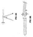
- Fig. 8B a plane m, called the midplane, exists whose length is unaffected by the deforming, and a straight line normal to the surface of the midplane remains normal to it and unchanged in length after deformation. Above and below the midplane, the plate is stretched or compressed by the applied deforming force. A series of uniformly spaced lines normal to the midplane is shown.
- the spacing of the lines at the top surface is changed, the displacement, or distortion, equal to ⁇ t, where ⁇ is the angle between the local normal to the midplane and the normal to the original undeformed midplane, and t is the distance from the midplane to the surface of the plate.
- ⁇ is the angle between the local normal to the midplane and the normal to the original undeformed midplane
- t is the distance from the midplane to the surface of the plate.
- the pattern is checked for errors and distortion in inspection and metrology tools. If distortion is too much, the reticle must be repaired or replaced. Distortion arising from mechanical deformation of the reticle should be distinguished from the intrinsic displacement errors created by the maskwriter tool however. If the reticle is chucked identically in both maskwriter and metrology tools, no distortion from mechanical deformation will occur, and if the reticle is chucked identically in the EUVL exposure tool, again no distortion from mechanical deformation will occur. In practice, some differences in chucking may occur, and these must be corrected for. This can be done by monitoring the flatness of the reticle when it is chucked.
- Differences in flatness can be related to distortion through the geometrical arguments above.
- the metrology tool measurements can then be compensated for the distortions added by the chucking differences, so that the distortions intrinsic to the maskwriter tool can be determined.
- any reticle flatness differences between the maskwriter tool and the EUVL tool will lead to additional distortions unless compensated for.
- This can be done with a EUVL reticle chuck whose flatness is adjustable, so that the reticle flatness can be corrected to that during the patterning in the maskwriter. This also requires a reticle flatness monitor in the EUVL tool.
- the component of the distortion lying in the plane of incidence of the illumination can be reduced and in some cases eliminated entirely. This is done essentially by using distortions arising from reticle deformation to cancel the distortions arising from height variations.
- the reticle surface is deformed, in general both the reticle height h' changes and the slope changes, as illustrated in Fig. 8B.
- the angle ⁇ for small deformations is just equal to the local slope of the reticle surface. Strictly speaking ⁇ is the component of the slope in the plane of incidence of the illumination.
- the distortion at the wafer caused by the deformation and the illumination non-telecentricity has a contribution from the height change h' which is given by h'tan ⁇ /M, as well as the actual distortion at the reticle which contributes an amount ⁇ t/M at the wafer.
- the total distortion at the wafer is then given by htan ⁇ /M + h'tan ⁇ /M + ⁇ t/M
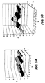
- Fig. 8C illustrates the correction of a height related distortion Zret by deforming the reticle surface by a function Zchuck using Eqs. 2 and 3.
- an error function can be constructed which is related to the X component of the residual distortion at the wafer: where the summations are over all points (x i , y j ) where Zret was measured.
- the function Zplane defines a flat plane whose position and orientation is optimized to help minimize Dx. It is explicitly separated from Zchuck, because in practice Zplane is likely to be set by adjusting the reticle stage orientation and height, rather than adjusting the reticle chuck shape, although the latter operation is also possible. By adjusting both Zplane and Zchuck to minimize Dx the X component of the residual distortion at the wafer can be minimized in the least squares sense.
- the total distortion at the wafer will in general include components in the X-direction (in the illumination plane of incidence) and the Y-direction. Since Zchuck(x) does not depend on y, no distortion of the reticle in the Y-direction will occur, so the Y-component of distortion at the wafer is not affected by this optimization.
- the X components of the distortion at the wafer will probably be greater than the Y components initially.
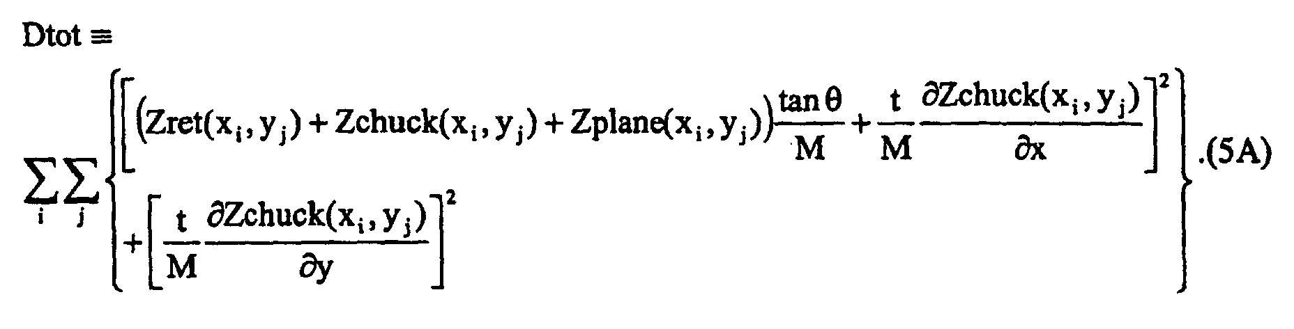
- the Y component of distortion at the wafer will inevitably increase in this case, but if the X component is reduced by a greater amount, the magnitude of the distortion will still be reduced. This requires defining a new error function which includes both X and Y components of distortion: Again, by adjusting both Zplane and Zchuck to minimize Dtot the magnitude of the residual distortion at the wafer can be minimized in the least squares sense.
- D POx (X i ,Y j ) is the X component of the distortion at the wafer introduced by the EUV projection optics
- X i and Y j are measured relative to the center of the image field
- (x i , y j ) is the point on the reticle corresponding to the position (X i , Y j ) in the image field
- the summation in i and j is only over the points lying within the image field, or equivalently the illumination field at the reticle.
- D POx (X i , Y j ) will be constant, but Zret(x i , y j ), Zchuck(x i , y j ), and Zplane(x i , y j ) will be changing, as different parts of the reticle are scanned through the illumination field.
- the optimization of Zchuck and Zplane must be constantly updated during the scanning.
- the distance t to the midplane may not be that of the reticle, because the chuck will impose some constraint on lateral motion of the mating reticle surface as the reticle is being deformed. If the reticle is held in intimate contact with the chuck, so that no relative lateral motion is possible, and if the chuck and reticle have the same material properties (as would be desirable from themal expansion considerations), t will be equal to half their combined thickness. If the reticle and chuck have different material properties, or if some lateral relative motion between them is possible, t will have to be determined in a more complicated manner, either empirically or by more sophisticated modeling.
- a deformable chuck may be applicable to the wafer 25 as well.
- the wafer is illuminated telecentrically and hence height variations do not lead to distortion, height variations will lead to defocus errors and may affect the balancing of aberrations.
- projection optics are not completely corrected for field curvature, even a flat wafer at the proper height will suffer some defocus error over the image field. Since field curvature increases away from the center of the field, it is likely to be more relevant in the direction normal to the scan, since the field dimension is greater in that direction.
- a static deformation can be applied to the wafer 25 using a deformable wafer chuck 20 which will place the entire illuminated part of the wafer 25 in the (curved) surface of best focus.
- the related distortion is t w ⁇ Zwafer(y w )/ ⁇ y, where t w is the distance from the wafer surface to the effective midplane of the wafer plus wafer chuck, and the location is measured in the coordinate system of the wafer chip (x w , y w ).
- an appropriate error function can be defined:
- the distortion for both components of the distortion at the wafer can be minimized in the least squares sense while still correcting for field curvature.
- Fig. 1A shows an EUV (or soft-X-ray SXR) system 110, including the aberration and distortion correcting system of this invention as described above.
- the depicted system is configured to perform microlithographic exposures in a step-and-scan manner.
- the EUV beam is produced by a laser-plasma source 117 excited by a laser 113 situated at the most upstream end of the depicted system 110.
- the laser 113 generates laser light at a wavelength within the range of near-infrared to visible.
- the laser 113 can be a YAG laser or an excimer laser.
- Laser light emitted from the laser 113 is condensed by a condensing optical system 115 and directed to the downstream laser-plasma source 117.
- the laser-plasma source 117 Upon receiving the laser light, the laser-plasma source 117 generates SXR (EUV) radiation having a wavelength ( ⁇ ) of approximately 13 nm with good efficiency.
- EUV SXR
- a nozzle (not shown), disposed near the laser-plasma source 117, discharges xenon gas in a manner such that the discharged xenon gas is irradiated with the laser light in the laser-plasma source 117.
- the laser light heats the discharged xenon gas to a temperature sufficiently high to produce a plasma that emits photons of EUV light as the irradiated xenon atoms transition to a lower-potential state.
- EUV light has low transmittance in air
- the optical path for EUV light propagating from the laser-plasma source 117 is contained in a vacuum chamber 119 normally evacuated to high vacuum. Since debris normally is produced in the vicinity of the nozzle discharging xenon gas, the vacuum chamber 119 desirably is separate from other chambers of the system.
- a parabolic mirror 121 coated with a Mo/Si multilayer film, is disposed relative to the laser-plasma source 117 so as to receive EUV light radiating from the laser-plasma source 117 and to reflect the EUV light in a downstream direction as a collimated beam.
- the collimated beam passes through a visible-light-blocking filter 123 situated downstream of the parabolic mirror 121.
- the filter 123 is made of Be, with a thickness of 0.15 ⁇ m.
- the filter 123 is contained in a vacuum chamber 125 evacuated to high vacuum.
- An exposure chamber 143 is disposed downstream of the filter 123.
- the exposure chamber 143 contains an illumination-optical system 127 that comprises a condenser mirror and a fly-eye mirror (not shown, but well understood in the art).
- the illumination-optical system 127 also is configured to trim the EUV beam (propagating from the filter 123) to have an arc-shaped transverse profile. The shaped "illumination beam" is irradiated toward the left in the figure.
- a circular, concave mirror 129 is situated so as to receive the illumination beam from the illumination-optical system 127.
- the concave mirror 129 has a parabolic reflective surface 129a and is mounted perpendicularly in the vacuum chamber 143.
- the concave mirror 129 comprises, for example, a quartz mirror substrate of which the reflection surface is machined extremely accurately to the desired parabolic configuration.
- the multilayer film can be of a first substance such as Ru (ruthenium) or Rh (rhodium) and a second substance such as Si, Be (Beryllium) or B 4 C (carbon tetraboride).
- a first substance such as Ru (ruthenium) or Rh (rhodium)
- a second substance such as Si, Be (Beryllium) or B 4 C (carbon tetraboride).
- a mirror 131 is situated at an angle relative to the concave mirror 129 so as to received the EUV beam from the concave mirror 129 and direct the beam at a low angle of incidence to a reflective reticle 133.
- the reticle 133 is disposed horizontally so that its reflective surface faces downward in the figure.
- the reticle 133 includes a multilayer film so as to be highly reflective to incident EUV light.
- a reticle pattern corresponding to the pattern to be transferred to a substrate 139, is defined in an EUV-absorbing layer formed on the multiplayer film of the reticle 133, as discussed later below.
- the reticle 133 is mounted via a reticle chuck on a reticle stage 135 that moves the reticle 133 at least in the Y direction.
- the reticle 133 normally is too large to be illuminated entirely during a single exposure "shot" of the EUV beam.
- successive regions of the reticle 133 can be irradiated sequentially so as to illuminate the pattern in a progressive manner with EUV light from the mirror 131.
- a projection-optical system 137 and substrate (such as a semiconductor wafer) 139 are disposed in that order downstream of the reticle 133.
- the projection-optical system 137 comprises multiple multilayer-film reflective mirrors that collectively demagnify an aerial image of the illuminated portion of the pattern on the reticle 133.
- the demagnification normally is according to a predetermined demagnification factor such as 1/4.
- the projection-optical system 137 focuses an aerial image of the illuminated pattern portion onto the surface of the substrate 139.
- the substrate 139 is mounted via a wafer (substrate) chuck on a substrate stage 141 that is movable in the X, Y, and Z directions.
- a preliminary-evacuation chamber 147 Connected to the exposure chamber 143 via a gate valve 145 is a preliminary-evacuation ("load-lock") chamber 147.
- the load-lock chamber 147 allows exchanges of the reticle 133 and/or substrate 139 as required.
- the load-lock chamber 147 is connected to a vacuum pump 149 that evacuates the load-lock chamber 147 to a vacuum level substantially equal to the vacuum level inside the exposure chamber 143.
- EUV light from the illumination-optical system 127 irradiates the reflective surface of the reticle 133.
- the reticle 133 and substrate 139 are moved by their respective stages 135 and 141 in a synchronous manner relative to the projection-optical system 137.
- the stages 135 and 141 move the reticle 133 and the substrate 139, respectively, at a velocity ratio determined by the demagnification factor of the projection-optical system 137.
- the entire circuit pattern defined don the reticle 133 is transferred, in a step-and-scan manner, to one or more "die” or "chip” locations on the substrate 139.
- each "die” or “chip” on the substrate 139 is a square having 25-mm sides.
- the pattern is thus” transferred” from the reticle 133 to the substrate at very high resolution (such as sufficient to resolve a 0.07- ⁇ m line-and-space (L/S) pattern). So as to be imprintable with the projected pattern, the upstream-facing surface of the substrate 139 is coated with a suitable "resist.”
- At least one multilayer-film optical element as described above is included in at least one of the illumination-optical system 127, the reticle 133, and the projection-optical system 137.
- Fig. 1C shows another embodiment of an X-ray (specifically EUV) microlithography system utilizing one or more multilayer-film reflective optical elements as described herein and comprising a EUV source S, an illumination-optical system (comprising elements GI and IR1-IR4), a reticle stage MST for holding a reticle M, a projection-optical system (comprising elements PR1-PR4) and a substrate stage WST for holding a substrate W (such as a semiconductor wafer).
- EUV source S an illumination-optical system
- a reticle stage MST for holding a reticle M
- a projection-optical system comprising elements PR1-PR4
- substrate stage WST for holding a substrate W (such as a semiconductor wafer).
- the EUV source S generates an illumination beam IB of EUV light.
- a laser LA generates and directs a high-intensity laser beam LB (near-IR to visible) through a lens L to the discharge region of a nozzle T that discharges a target substance such as xenon.
- the irradiated target substance forms a plasma that emit photons of EUV light that constitute the illumination beam IB.
- the illumination beam IB is reflected by a parabolic multilayer-film mirror PM to a window W1.
- the EUV source S is contained in a chamber C1 that is evacuated to a suitably high vacuum by means of a vacuum pump (not shown).
- the illumination beam IB passes through the window W1 to the interior of an optical-system chamber C2.
- the illumination beam IB then propagates to the illumination-optical system comprising mirrors GI, IR1, IR2, IR3 and IR4.
- the mirror GI is a grazing-incidence mirror that reflects the grazing-incident illumination beam IB from the EUV source S.
- the mirror GI can be a multilayer-film mirror.
- the mirrors IR1, IR2, IR3 and IR4 are multilayer-film mirrors each including a surface multilayer film exhibiting high reflectivity to incident EUV radiation, as described elsewhere herein.
- the illumination-optical system also comprises a filter (not shown) that is transmissive only to EUV radiation of a prescribed wavelength.
- the illumination-optical system directs the illumination beam IB, having the desired wavelength, to a selected region on the reticle M.
- the reticle M is a reflective reticle including a multilayer film.
- the beam reflected from the reticle M carries an aerial image of the illuminated region of the reticle M; hence the reflected beam is termed a patterned beam.
- the protection-optical system comprises multiple multilayer-film mirrors PR1, PR2, PR3 and PR4 that collectively project an image of the illuminated portion of the reticle M onto a corresponding location on the substrate W.
- the pattern defined by the reticle M is transfer-exposed onto the substrate W.
- several of the mirrors PR1-PR4 (specially the mirrors PR1 and PR4) have a cutout allowing the patterned beam unobstructed passage in the projection-optical system.
- the substrate W is coated with an exposure-sensitive resist. Since EUV radiation is absorbed and attenuated in the atmosphere, the environment in the optical-system chamber C2 is maintained at a suitably high vacuum (such as 10 -5 Torr or less).
- the substrate W can be performed in a "step-and-repeat,” “step-and-scan,” or pure s canning-exposure manner, or other suitable manner, all of which involving controlled movements of the reticle stage MST and substrate stage WST relative to each other as transfer-exposure of the pattern progresses.
- the substrate W is situated in a separate chamber C3, termed a "substrate chamber” or “wafer chamber,” that contains the substrate stage WST.
- the patterned beam PB enters the substrate chamber C3 from the optical-system chamber C2, the beam passes through a window W2.
- Wavefront aberration must be controlled so as to satisfy a given specification but a wavefront aberration correction system of this invention can be used to a correct such wavefront aberration errors.
- Wavefront aberration can be measured either in situ or outside the system.
- a device for measuring wavefront aberration of a EUV projection-optical system is described, for example, in the U.S patent 6,266,389 issued July 24, 2001, which is herein incorporated by reference.
- the surface shape of a mirror is varied such that the measured wavefront aberration comes to satisfy the given specification but it is not necessary to vary the surface configurations of all of the mirrors. It is sufficient if the surface configuration of at least one of the mirrors is made adjustable.
- a method of obtaining the final surface configuration of the mirror from the measured wavefront aberration is also described in aforementioned U.S patent 6,266,389.
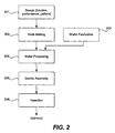
- step 301 the device's function and performance characteristics are designed.
- step 302 a mask (reticle) having a pattern is designed according to the previous designing step, and in a parallel step 303, a wafer is made from a silicon material.
- the mask pattern designed in step 302 is exposed onto the wafer from step 303 in step 304 by a photolithography system such as the systems described above.
- step 305 the semiconductor device is assembled (including the dicing process, bonding process and packaging process), then finally the device is inspected in step 306.
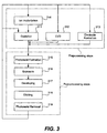
- Fig. 3 illustrates a detailed flowchart example of the above-mentioned step 304 in the case of fabricating semiconductor devices.
- step 311 oxidation step
- step 312 CVD step
- step 313 electrode formation step
- step 314 ion implantation step
- steps 311-314 form the preprocessing steps for wafers during wafer processing, and selection is made at each step according to processing requirements.
- step 315 photoresist formation step
- step 316 exposure step
- step 317 developer step
- step 318 etching step
- steps 319 photoresist removal step
Landscapes
- Physics & Mathematics (AREA)
- General Physics & Mathematics (AREA)
- Health & Medical Sciences (AREA)
- Toxicology (AREA)
- Life Sciences & Earth Sciences (AREA)
- Atmospheric Sciences (AREA)
- Engineering & Computer Science (AREA)
- Environmental & Geological Engineering (AREA)
- Epidemiology (AREA)
- Public Health (AREA)
- Optics & Photonics (AREA)
- Exposure And Positioning Against Photoresist Photosensitive Materials (AREA)
- Exposure Of Semiconductors, Excluding Electron Or Ion Beam Exposure (AREA)
- Preparing Plates And Mask In Photomechanical Process (AREA)
Abstract
Description





Claims (20)
- A system for correcting aberration and distortion in EUV lithography, said system comprising:wherein said deformable reticle chuck and said deformable mirror are controlled such that aberration and distortion of an image of said reticle formed on said wafer by said optical system are corrected based on the height measured by said reticle height sensor.a deformable reticle chuck that has a reticle placed thereon;a reticle height sensor that measures a height of the reticle placed on said deformable reticle chuck;an optical system that has an exit pupil, projects EUV radiation onto the reticle placed on said reticle chuck and leads reflected EUV radiation from said reticle through said exit pupil onto a wafer placed on a wafer chuck; said optical system including a deformable mirror proximal to said exit pupil;
- The system of claim 1 further comprising a wafer height sensor that detects a height of said wafer, wherein aberration and distortion of the image are corrected based also on the height measured by said wafer height sensor.
- The system of claim 1 wherein said wafer chuck is deformable and deformation and distortion of the image are corrected also by deforming said wafer chuck.
- The system of claim 1 wherein said reticle has an electrically conductive coating thereon and said deformable reticle chuck comprises:a supporting structure having a top surface;a deformable membrane disposed above said supporting structure, said deformable membrane comprising a dielectric layer of a dielectric material and a conductive layer of an electrically conductive material;a voltage source connected to said conductive coating of said reticle and said conductive layer to generate an electrostatic attractive force therebetween;a plurality of actuator rods each connected to a corresponding one of actuators, said actuator rods penetrating said supporting structure and protruding above said top surface, said actuator rods supporting and contacting said membrane, leaving a chamber between said membrane and said top surface of said supporting structure; anda coolant gas inside said chamber.
- The system of claim 4 wherein said supporting structure has throughholes through which a coolant fluid is passed.
- The system of claim 4 further comprising a clamping plate for clamping said actuator rods in place after said actuator rods are adjusted.
- A method of correcting aberration and distortion in EUV lithography, said method comprising the steps of:placing a reticle on a deformable reticle chuck;measuring heights of said reticle by a reticle height sensor;projecting EUV radiation onto said reticle and leading reflected EUV radiation from said reticle through an exit pupil of an optical system onto a wafer placed on a wafer chuck, said optical system including a deformable mirror proximal to said exit pupil;controlling said deformable reticle chuck and thereby correcting aberration and distortion of an image of said reticle formed on said wafer by said optical system based on the height measured by said reticle height sensor.
- The method of claim 7 wherein said deformable reticle chuck comprises:a supporting structure having a top surface;a deformable membrane disposed above said supporting structure, said deformable membrane comprising a dielectric layer of a dielectric material and a conductive layer of an electrically conductive material;a voltage source connected to said conductive coating of said reticle and said conductive layer to generate an electrostatic attractive force therebetween;a plurality of actuator rods each connected to a corresponding one of actuators, said actuator rods penetrating said supporting structure and protruding above said top surface, said actuator rods supporting and contacting said membrane, leaving a chamber between said membrane and said top surface of said supporting structure; anda coolant gas inside said chamber.
- The method of claim 8 further comprising the step of passing a coolant fluid through a throughhole formed through said supporting structure.
- The method of claim 8 further comprising the step of clamping said actuator rods in place after adjusting said actuator rods.
- The method of claim 7 further comprising the step of adjusting said deformable mirror proximal to said exit pupil and thereby correcting aberration and distortion of said image of said reticle formed on said wafer by said optical system.
- The method of claim 7 further comprising the step of measuring a height of said wafer by means of a wafer height sensor and thereby correcting aberration and distortion of said image of said reticle formed on said wafer by said optical system.
- A deformable reticle chuck for placing thereon a reticle having an electrically conductive coating, said chuck comprising:a supporting structure having a top surface;a deformable membrane disposed above said supporting structure, said deformable membrane comprising a dielectric layer of a dielectric material and a conductive layer of an electrically conductive material;a voltage source connected to said conductive coating of said reticle and said conductive layer to generate an electrostatic attractive force therebetween;a plurality of actuator rods each connected to a corresponding one of actuators, said actuator rods penetrating said supporting structure and protruding above said top surface, said actuator rods supporting and contacting said membrane, leaving a chamber between said membrane and said top surface of said supporting structure; anda coolant gas inside said chamber.
- The deformable reticle chuck of claim 13 wherein said supporting structure has throughholes through which a coolant fluid is passed.
- The deformable reticle chuck of claim 13 further comprising a clamping plate for clamping said actuator rods in place after said actuator rods are adjusted.
- A lithography system comprising:wherein said deformable reticle chuck and said deformable mirror are controlled such that aberration and distortion of an image of said reticle formed on said wafer by said optical system are corrected based on the height measured by said reticle height sensor.an illumination source;a deformable reticle chuck that has a reticle placed thereon;a reticle height sensor that measures a height of the reticle placed on said deformable reticle chuck;a wafer chuck having a wafer placed thereon;an optical system that has an exit pupil, projects EUV radiation from said illumination source onto the reticle placed on said reticle chuck and leads reflected EUV radiation from said reticle through said exit pupil onto said wafer placed on said wafer chuck, said optical system including a deformable mirror proximal to said exit pupil; andan enclosure that surrounds at least a portion of said wafer chuck, the enclosure having a sealing surface;
- An object manufactured with the lithography system of claim 16.
- A wafer on which an image has been formed by the lithography system of claim 16.
- A method for making an object using a lithography process, wherein the lithography process utilizes a lithography system as recited in claim 16.
- A method for patterning a wafer using a lithography process, wherein the lithography process utilizes a lithography system as recited in claim 16.
Applications Claiming Priority (4)
| Application Number | Priority Date | Filing Date | Title |
|---|---|---|---|
| US39105902P | 2002-06-21 | 2002-06-21 | |
| US39088002P | 2002-06-21 | 2002-06-21 | |
| US390880P | 2002-06-21 | ||
| US391059P | 2002-06-21 |
Publications (2)
| Publication Number | Publication Date |
|---|---|
| EP1376238A2 true EP1376238A2 (en) | 2004-01-02 |
| EP1376238A3 EP1376238A3 (en) | 2009-07-08 |
Family
ID=29718540
Family Applications (1)
| Application Number | Title | Priority Date | Filing Date |
|---|---|---|---|
| EP03013978A Withdrawn EP1376238A3 (en) | 2002-06-21 | 2003-06-20 | A system for correcting aberration and distortion in EUV litography |
Country Status (3)
| Country | Link |
|---|---|
| US (1) | US6897940B2 (en) |
| EP (1) | EP1376238A3 (en) |
| JP (1) | JP2004031954A (en) |
Cited By (6)
| Publication number | Priority date | Publication date | Assignee | Title |
|---|---|---|---|---|
| EP1801654A1 (en) * | 2005-12-23 | 2007-06-27 | ASML Netherlands B.V. | Lithographic apparatus and device manufacturing method |
| WO2010094684A1 (en) * | 2009-02-17 | 2010-08-26 | Carl Zeiss Smt Ag | Projection exposure apparatus comprising an actuator system |
| WO2011000689A1 (en) * | 2009-06-30 | 2011-01-06 | Asml Holding N.V. | Image-compensating addressable electrostatic chuck system |
| TWI643029B (en) * | 2015-12-25 | 2018-12-01 | 佳能股份有限公司 | Evaluation method, exposure method, and article manufacturing method |
| WO2020161235A1 (en) * | 2019-02-06 | 2020-08-13 | Carl Zeiss Smt Gmbh | Device and method for determining placements of pattern elements of a reflective photolithographic mask in the operating environment thereof |
| WO2024083404A1 (en) * | 2022-10-19 | 2024-04-25 | Asml Netherlands B.V. | Lithographic apparatus and method |
Families Citing this family (44)
| Publication number | Priority date | Publication date | Assignee | Title |
|---|---|---|---|---|
| DE10216786C5 (en) * | 2002-04-15 | 2009-10-15 | Ers Electronic Gmbh | Method and apparatus for conditioning semiconductor wafers and / or hybrids |
| DE10258715B4 (en) * | 2002-12-10 | 2006-12-21 | Carl Zeiss Smt Ag | Method for producing an optical imaging system |
| US7022443B2 (en) * | 2003-02-12 | 2006-04-04 | Intel Corporation | Compensation of reflective mask effects in lithography systems |
| US7125128B2 (en) * | 2004-01-26 | 2006-10-24 | Nikon Corporation | Adaptive-optics actuator arrays and methods for using such arrays |
| DE102004010002B4 (en) * | 2004-03-01 | 2007-10-31 | Infineon Technologies Ag | Mask holder for holding a lithographic reflection mask and method |
| JP4157486B2 (en) | 2004-03-24 | 2008-10-01 | 株式会社東芝 | Method for generating drawing pattern data and mask drawing method |
| US20050223973A1 (en) * | 2004-03-30 | 2005-10-13 | Infineon Technologies Ag | EUV lithography system and chuck for releasing reticle in a vacuum isolated environment |
| US7463336B2 (en) * | 2004-04-14 | 2008-12-09 | Asml Netherlands B.V. | Device manufacturing method and apparatus with applied electric field |
| FR2877104B1 (en) * | 2004-10-27 | 2006-12-29 | Sagem | IMAGING OR INSULATION DEVICE, IN PARTICULAR FOR CARRYING OUT AN ELECTRON MICRO CIRCUIT |
| US7184124B2 (en) * | 2004-10-28 | 2007-02-27 | Asml Holding N.V. | Lithographic apparatus having an adjustable projection system and device manufacturing method |
| US7834975B2 (en) * | 2004-12-27 | 2010-11-16 | Asml Netherlands B.V. | Method and exposure apparatus for performing a tilted focus and a device manufactured accordingly |
| US7518706B2 (en) | 2004-12-27 | 2009-04-14 | Asml Netherlands B.V. | Exposure apparatus, a tilting device method for performing a tilted focus test, and a device manufactured accordingly |
| US20060138349A1 (en) * | 2004-12-27 | 2006-06-29 | Asml Netherlands B.V. | Lithographic apparatus and device manufacturing method |
| US7436484B2 (en) * | 2004-12-28 | 2008-10-14 | Asml Netherlands B.V. | Lithographic apparatus and device manufacturing method |
| TWI355570B (en) * | 2005-06-07 | 2012-01-01 | Ricoh Co Ltd | Toner container and image forming apparatus |
| US7518703B2 (en) * | 2005-06-28 | 2009-04-14 | Asml Netherlands B.V. | Lithographic apparatus and method |
| US7446855B2 (en) * | 2005-07-25 | 2008-11-04 | Micron Technology, Inc | Methods and apparatuses for configuring radiation in microlithographic processing of workpieces using an adjustment structure |
| US7643130B2 (en) * | 2005-11-04 | 2010-01-05 | Nuflare Technology, Inc. | Position measuring apparatus and positional deviation measuring method |
| KR100809329B1 (en) * | 2006-09-08 | 2008-03-07 | 삼성전자주식회사 | Photolithography apparatus including a mirror for correcting the aberration of the optical system and the mirror including the aberration correction unit |
| US7817252B2 (en) * | 2006-09-29 | 2010-10-19 | Intel Corporation | Holder for carrying a photolithography mask in a flattened condition |
| US7853067B2 (en) | 2006-10-27 | 2010-12-14 | Asml Holding N.V. | Systems and methods for lithographic reticle inspection |
| JP4814782B2 (en) * | 2006-12-28 | 2011-11-16 | 株式会社ジェイテック | X-ray focusing method and apparatus using phase recovery method |
| US7759024B2 (en) * | 2007-02-28 | 2010-07-20 | Intel Corporation | Controlling shape of a reticle with low friction film coating at backside |
| US7894038B2 (en) * | 2007-03-14 | 2011-02-22 | Asml Netherlands B.V. | Device manufacturing method, lithographic apparatus, and a computer program |
| US8975599B2 (en) * | 2007-05-03 | 2015-03-10 | Asml Netherlands B.V. | Image sensor, lithographic apparatus comprising an image sensor and use of an image sensor in a lithographic apparatus |
| DE102008002377A1 (en) * | 2007-07-17 | 2009-01-22 | Carl Zeiss Smt Ag | Illumination system and projection exposure apparatus for microlithography with such a lighting system |
| JPWO2009125867A1 (en) * | 2008-04-11 | 2011-08-04 | 株式会社ニコン | Stage apparatus, exposure apparatus, and device manufacturing method |
| NL2003673A (en) * | 2008-11-21 | 2010-05-25 | Asml Netherlands Bv | Lithographic apparatus and methods for compensating substrate unflatness, determining the effect of patterning device unflatness, and determing the effect of thermal loads on a patterning device. |
| KR101640766B1 (en) * | 2009-12-01 | 2016-07-20 | 삼성전자주식회사 | Reflective Reticle Chuck and Reflective Illumination System including the Same, Method of Improving Flatness of Reflective Reticle and Manufacturing Semiconductor Device Using the Same |
| NL2006190A (en) * | 2010-03-11 | 2011-09-13 | Asml Netherlands Bv | Lithographic apparatus and device manufacturing method. |
| US20120026480A1 (en) * | 2010-07-26 | 2012-02-02 | Asml Netherlands B.V. | Image-Compensating Addressable Electrostatic Chuck System |
| EP2434345B1 (en) * | 2010-09-27 | 2013-07-03 | Imec | Method and system for evaluating euv mask flatness |
| DE102010041556A1 (en) | 2010-09-28 | 2012-03-29 | Carl Zeiss Smt Gmbh | Projection exposure apparatus for microlithography and method for microlithographic imaging |
| DE102010043498A1 (en) * | 2010-11-05 | 2012-05-10 | Carl Zeiss Smt Gmbh | Projection objective of a microlithographic projection exposure apparatus designed for EUV, and method for optical adjustment of a projection objective |
| JP2012142619A (en) * | 2012-04-11 | 2012-07-26 | Renesas Electronics Corp | Reflective exposure method |
| US20140253887A1 (en) * | 2013-03-07 | 2014-09-11 | Applied Materials, Inc. | Contamination prevention for photomask in extreme ultraviolet lithography application |
| JP6236095B2 (en) | 2013-03-13 | 2017-11-22 | カール・ツァイス・エスエムティー・ゲーエムベーハー | Microlithography equipment |
| US9476764B2 (en) | 2013-09-10 | 2016-10-25 | Taiwan Semiconductor Manufacturing Co., Ltd. | Wavefront adjustment in extreme ultra-violet (EUV) lithography |
| US9405204B2 (en) | 2013-09-18 | 2016-08-02 | Taiwan Semiconductor Manufacturing Co., Ltd. | Method of overlay in extreme ultra-violet (EUV) lithography |
| US9034665B2 (en) * | 2013-10-11 | 2015-05-19 | Taiwan Semiconductor Manufacturing Co., Ltd. | Tool configuration and method for extreme ultra-violet (EUV) patterning with a deformable reflective surface |
| JP6647198B2 (en) * | 2013-12-22 | 2020-02-14 | アプライド マテリアルズ インコーポレイテッドApplied Materials,Incorporated | Extreme ultraviolet lithography system with chuck assembly and method of manufacturing the same |
| DE102014218474A1 (en) * | 2014-09-15 | 2016-03-17 | Carl Zeiss Smt Gmbh | Projection objective, projection exposure apparatus and projection exposure method for EUV microlithography |
| US20170363952A1 (en) | 2014-12-19 | 2017-12-21 | Hoya Corporation | Mask blank substrate, mask blank, and methods for manufacturing them, method for manufacturing transfer mask, and method for manufacturing semiconductor device |
| DE102015225262A1 (en) * | 2015-12-15 | 2017-06-22 | Carl Zeiss Smt Gmbh | Optical system, in particular for a microlithographic projection exposure apparatus |
Family Cites Families (24)
| Publication number | Priority date | Publication date | Assignee | Title |
|---|---|---|---|---|
| US4003640A (en) * | 1975-06-23 | 1977-01-18 | Hughes Aircraft Company | Electro-hydraulic driver for deformable face plate |
| DE3238108A1 (en) | 1982-10-14 | 1984-04-19 | Messerschmitt-Bölkow-Blohm GmbH, 8000 München | ADAPTIVE OPTICAL SYSTEM |
| DE3502025A1 (en) * | 1985-01-23 | 1986-07-24 | Diehl GmbH & Co, 8500 Nürnberg | DEFORMABLE MIRROR |
| US4737621A (en) * | 1985-12-06 | 1988-04-12 | Adaptive Optics Assoc., Inc. | Integrated adaptive optical wavefront sensing and compensating system |
| US4875765A (en) * | 1988-07-29 | 1989-10-24 | Eastman Kodak Company | Method for correction of distortions of a mirror |
| JP2690960B2 (en) * | 1988-09-07 | 1997-12-17 | 株式会社日立製作所 | Magnification projection exposure method and apparatus |
| US5026977A (en) * | 1989-04-05 | 1991-06-25 | The Charles Stark Draper Laboratory, Inc. | Wavefront sensing and correction with deformable mirror |
| US5005961A (en) * | 1989-12-19 | 1991-04-09 | Eastman Kodak Company | Device for converting a displacement in a direction into a force in the same direction |
| US5142132A (en) * | 1990-11-05 | 1992-08-25 | Litel Instruments | Adaptive optic wafer stepper illumination system |
| US5229889A (en) * | 1991-12-10 | 1993-07-20 | Hughes Aircraft Company | Simple adaptive optical system |
| US5793473A (en) * | 1994-06-09 | 1998-08-11 | Nikon Corporation | Projection optical apparatus for projecting a mask pattern onto the surface of a target projection object and projection exposure apparatus using the same |
| US5745309A (en) * | 1994-06-13 | 1998-04-28 | The United States Of America As Represented By The United States Department Of Energy | Method for removing tilt control in adaptive optics systems |
| WO1997033247A1 (en) * | 1996-03-07 | 1997-09-12 | Accu-Sort Systems, Inc. | Dynamic focusing apparatus for optical imaging systems |
| US6235438B1 (en) * | 1997-10-07 | 2001-05-22 | Nikon Corporation | Projection exposure method and apparatus |
| JPH11345761A (en) * | 1998-05-29 | 1999-12-14 | Nikon Corp | Scanning exposure equipment |
| DE19824030A1 (en) | 1998-05-29 | 1999-12-02 | Zeiss Carl Fa | Catadioptric projection lens with adaptive mirror and projection exposure method |
| US5986795A (en) * | 1998-06-15 | 1999-11-16 | Chapman; Henry N. | Deformable mirror for short wavelength applications |
| US6166865A (en) * | 1999-05-19 | 2000-12-26 | Nikon Corporation | Projection optical system and exposure apparatus |
| US6229871B1 (en) * | 1999-07-20 | 2001-05-08 | Euv Llc | Projection lithography with distortion compensation using reticle chuck contouring |
| TW508653B (en) * | 2000-03-24 | 2002-11-01 | Asml Netherlands Bv | Lithographic projection apparatus and integrated circuit manufacturing method |
| TW575771B (en) * | 2000-07-13 | 2004-02-11 | Asml Netherlands Bv | Lithographic apparatus, device manufacturing method, and device manufactured thereby |
| DE10051466C2 (en) * | 2000-10-17 | 2002-09-19 | Infineon Technologies Ag | Arrangement as a mask for lithography |
| DE60206908T2 (en) | 2001-01-09 | 2006-07-20 | Carl Zeiss Smt Ag | PROJECTION SYSTEM FOR EXTREME ULTRAVIOLETT LITHOGRAPHY |
| EP1231513A1 (en) | 2001-02-08 | 2002-08-14 | Asm Lithography B.V. | Lithographic projection apparatus with adjustable focal surface |
-
2003
- 2003-06-04 US US10/455,254 patent/US6897940B2/en not_active Expired - Fee Related
- 2003-06-19 JP JP2003174518A patent/JP2004031954A/en active Pending
- 2003-06-20 EP EP03013978A patent/EP1376238A3/en not_active Withdrawn
Cited By (11)
| Publication number | Priority date | Publication date | Assignee | Title |
|---|---|---|---|---|
| EP1801654A1 (en) * | 2005-12-23 | 2007-06-27 | ASML Netherlands B.V. | Lithographic apparatus and device manufacturing method |
| US7961291B2 (en) | 2005-12-23 | 2011-06-14 | Asml Netherlands B.V. | Lithographic apparatus and device manufacturing method |
| WO2010094684A1 (en) * | 2009-02-17 | 2010-08-26 | Carl Zeiss Smt Ag | Projection exposure apparatus comprising an actuator system |
| US9030644B2 (en) | 2009-02-17 | 2015-05-12 | Carl Zeiss Smt Gmbh | Projection exposure apparatus for semiconductor lithography including an actuator system |
| WO2011000689A1 (en) * | 2009-06-30 | 2011-01-06 | Asml Holding N.V. | Image-compensating addressable electrostatic chuck system |
| US8477472B2 (en) | 2009-06-30 | 2013-07-02 | Asml Holding N.V. | Image-compensating addressable electrostatic chuck system |
| KR101407477B1 (en) * | 2009-06-30 | 2014-06-16 | 에이에스엠엘 홀딩 엔.브이. | Image-compensating addressable electrostatic chuck system |
| TWI643029B (en) * | 2015-12-25 | 2018-12-01 | 佳能股份有限公司 | Evaluation method, exposure method, and article manufacturing method |
| WO2020161235A1 (en) * | 2019-02-06 | 2020-08-13 | Carl Zeiss Smt Gmbh | Device and method for determining placements of pattern elements of a reflective photolithographic mask in the operating environment thereof |
| US12321091B2 (en) | 2019-02-06 | 2025-06-03 | Carl Zeiss Smt Gmbh | Device and method for determining placements of pattern elements of a reflective photolithographic mask in the operating environment thereof |
| WO2024083404A1 (en) * | 2022-10-19 | 2024-04-25 | Asml Netherlands B.V. | Lithographic apparatus and method |
Also Published As
| Publication number | Publication date |
|---|---|
| US20040013956A1 (en) | 2004-01-22 |
| EP1376238A3 (en) | 2009-07-08 |
| JP2004031954A (en) | 2004-01-29 |
| US6897940B2 (en) | 2005-05-24 |
Similar Documents
| Publication | Publication Date | Title |
|---|---|---|
| US6897940B2 (en) | System for correcting aberrations and distortions in EUV lithography | |
| US6803994B2 (en) | Wavefront aberration correction system | |
| CN100375238C (en) | Exposure equipment and device manufacturing method using the exposure equipment | |
| JP2004064076A (en) | Deformable mirror structure, control method of deformable mirror, and exposure apparatus | |
| WO1999045581A1 (en) | Method and apparatus for exposure, method of manufacture of exposure tool, device, and method of manufacture of device | |
| JP2002246309A (en) | Lithographic apparatus, device manufacturing method, and device manufactured by the method | |
| US7348582B2 (en) | Light source apparatus and exposure apparatus having the same | |
| WO2002052620A1 (en) | Wavefront aberration measuring instrument, wavefront aberration measuring method, exposure apparatus, and method for manufacturing microdevice | |
| US6843572B2 (en) | Form-error-cancelling mirror-support devices and related methods, and microlithography systems comprising same | |
| US20050140947A1 (en) | Exposure apparatus and device manufacturing method | |
| TW200527154A (en) | Lithographic apparatus and device manufacturing method | |
| US9030645B2 (en) | Illumination optical system, exposure apparatus, and exposure method | |
| KR20120108960A (en) | Image-Compensation Addressable Electrostatic Chuck System | |
| JP2005117048A (en) | Lithography equipment and device manufacturing method | |
| US20110044425A1 (en) | Spectral purity filters for use in a lithographic apparatus | |
| US20070285632A1 (en) | EUVL reticle stage and reticle protection system and method | |
| JP2002318334A (en) | Method of holding reflector, reflector and exposure apparatus | |
| JP4705843B2 (en) | Lithographic apparatus and device manufacturing method | |
| US20050219549A1 (en) | Measuring apparatus and method | |
| US5335259A (en) | X-ray exposure apparatus | |
| US20050221238A1 (en) | Use of a reticle absorber material in reducing aberrations | |
| JP3958261B2 (en) | Optical system adjustment method | |
| US12158706B2 (en) | Lithographic apparatus and method with improved contaminant particle capture | |
| JP2006114914A (en) | Lithographic system, method for adjusting transmission characteristics of an optical path in a lithographic system, semiconductor device, method for manufacturing a reflective element for use in a lithographic system, and reflective element manufactured thereby | |
| US20050279951A1 (en) | Grazing incidence mirror, lithographic apparatus including a grazing incidence mirror, method for providing a grazing incidence mirror, method for enhancing EUV reflection of a grazing incidence mirror, device manufacturing method and device manufactured thereby |
Legal Events
| Date | Code | Title | Description |
|---|---|---|---|
| PUAI | Public reference made under article 153(3) epc to a published international application that has entered the european phase |
Free format text: ORIGINAL CODE: 0009012 |
|
| AK | Designated contracting states |
Kind code of ref document: A2 Designated state(s): AT BE BG CH CY CZ DE DK EE ES FI FR GB GR HU IE IT LI LU MC NL PT RO SE SI SK TR |
|
| AX | Request for extension of the european patent |
Extension state: AL LT LV MK |
|
| PUAL | Search report despatched |
Free format text: ORIGINAL CODE: 0009013 |
|
| AK | Designated contracting states |
Kind code of ref document: A3 Designated state(s): AT BE BG CH CY CZ DE DK EE ES FI FR GB GR HU IE IT LI LU MC NL PT RO SE SI SK TR |
|
| AX | Request for extension of the european patent |
Extension state: AL LT LV MK |
|
| AKX | Designation fees paid | ||
| STAA | Information on the status of an ep patent application or granted ep patent |
Free format text: STATUS: THE APPLICATION IS DEEMED TO BE WITHDRAWN |
|
| 18D | Application deemed to be withdrawn |
Effective date: 20100105 |
|
| REG | Reference to a national code |
Ref country code: DE Ref legal event code: 8566 |