EP1376190A1 - Optical switch - Google Patents
Optical switch Download PDFInfo
- Publication number
- EP1376190A1 EP1376190A1 EP02714494A EP02714494A EP1376190A1 EP 1376190 A1 EP1376190 A1 EP 1376190A1 EP 02714494 A EP02714494 A EP 02714494A EP 02714494 A EP02714494 A EP 02714494A EP 1376190 A1 EP1376190 A1 EP 1376190A1
- Authority
- EP
- European Patent Office
- Prior art keywords
- optical switch
- cells
- cell
- punch
- piezoelectric
- Prior art date
- Legal status (The legal status is an assumption and is not a legal conclusion. Google has not performed a legal analysis and makes no representation as to the accuracy of the status listed.)
- Granted
Links
Images






Classifications
-
- B—PERFORMING OPERATIONS; TRANSPORTING
- B41—PRINTING; LINING MACHINES; TYPEWRITERS; STAMPS
- B41J—TYPEWRITERS; SELECTIVE PRINTING MECHANISMS, i.e. MECHANISMS PRINTING OTHERWISE THAN FROM A FORME; CORRECTION OF TYPOGRAPHICAL ERRORS
- B41J2/00—Typewriters or selective printing mechanisms characterised by the printing or marking process for which they are designed
- B41J2/005—Typewriters or selective printing mechanisms characterised by the printing or marking process for which they are designed characterised by bringing liquid or particles selectively into contact with a printing material
- B41J2/01—Ink jet
- B41J2/135—Nozzles
- B41J2/16—Production of nozzles
- B41J2/1607—Production of print heads with piezoelectric elements
- B41J2/1609—Production of print heads with piezoelectric elements of finger type, chamber walls consisting integrally of piezoelectric material
-
- B—PERFORMING OPERATIONS; TRANSPORTING
- B41—PRINTING; LINING MACHINES; TYPEWRITERS; STAMPS
- B41J—TYPEWRITERS; SELECTIVE PRINTING MECHANISMS, i.e. MECHANISMS PRINTING OTHERWISE THAN FROM A FORME; CORRECTION OF TYPOGRAPHICAL ERRORS
- B41J2/00—Typewriters or selective printing mechanisms characterised by the printing or marking process for which they are designed
- B41J2/005—Typewriters or selective printing mechanisms characterised by the printing or marking process for which they are designed characterised by bringing liquid or particles selectively into contact with a printing material
- B41J2/01—Ink jet
- B41J2/135—Nozzles
- B41J2/16—Production of nozzles
- B41J2/1621—Manufacturing processes
- B41J2/1623—Manufacturing processes bonding and adhesion
-
- B—PERFORMING OPERATIONS; TRANSPORTING
- B41—PRINTING; LINING MACHINES; TYPEWRITERS; STAMPS
- B41J—TYPEWRITERS; SELECTIVE PRINTING MECHANISMS, i.e. MECHANISMS PRINTING OTHERWISE THAN FROM A FORME; CORRECTION OF TYPOGRAPHICAL ERRORS
- B41J2/00—Typewriters or selective printing mechanisms characterised by the printing or marking process for which they are designed
- B41J2/005—Typewriters or selective printing mechanisms characterised by the printing or marking process for which they are designed characterised by bringing liquid or particles selectively into contact with a printing material
- B41J2/01—Ink jet
- B41J2/135—Nozzles
- B41J2/16—Production of nozzles
- B41J2/1621—Manufacturing processes
- B41J2/1632—Manufacturing processes machining
-
- F—MECHANICAL ENGINEERING; LIGHTING; HEATING; WEAPONS; BLASTING
- F04—POSITIVE - DISPLACEMENT MACHINES FOR LIQUIDS; PUMPS FOR LIQUIDS OR ELASTIC FLUIDS
- F04B—POSITIVE-DISPLACEMENT MACHINES FOR LIQUIDS; PUMPS
- F04B43/00—Machines, pumps, or pumping installations having flexible working members
- F04B43/02—Machines, pumps, or pumping installations having flexible working members having plate-like flexible members, e.g. diaphragms
- F04B43/04—Pumps having electric drive
- F04B43/043—Micropumps
- F04B43/046—Micropumps with piezoelectric drive
-
- G—PHYSICS
- G02—OPTICS
- G02B—OPTICAL ELEMENTS, SYSTEMS OR APPARATUS
- G02B6/00—Light guides; Structural details of arrangements comprising light guides and other optical elements, e.g. couplings
- G02B6/24—Coupling light guides
- G02B6/26—Optical coupling means
- G02B6/35—Optical coupling means having switching means
- G02B6/3538—Optical coupling means having switching means based on displacement or deformation of a liquid
-
- B—PERFORMING OPERATIONS; TRANSPORTING
- B41—PRINTING; LINING MACHINES; TYPEWRITERS; STAMPS
- B41J—TYPEWRITERS; SELECTIVE PRINTING MECHANISMS, i.e. MECHANISMS PRINTING OTHERWISE THAN FROM A FORME; CORRECTION OF TYPOGRAPHICAL ERRORS
- B41J2202/00—Embodiments of or processes related to ink-jet or thermal heads
- B41J2202/01—Embodiments of or processes related to ink-jet heads
- B41J2202/11—Embodiments of or processes related to ink-jet heads characterised by specific geometrical characteristics
-
- G—PHYSICS
- G02—OPTICS
- G02B—OPTICAL ELEMENTS, SYSTEMS OR APPARATUS
- G02B6/00—Light guides; Structural details of arrangements comprising light guides and other optical elements, e.g. couplings
- G02B6/24—Coupling light guides
- G02B6/26—Optical coupling means
- G02B6/35—Optical coupling means having switching means
- G02B6/351—Optical coupling means having switching means involving stationary waveguides with moving interposed optical elements
- G02B6/3522—Optical coupling means having switching means involving stationary waveguides with moving interposed optical elements the optical element enabling or impairing total internal reflection
-
- G—PHYSICS
- G02—OPTICS
- G02B—OPTICAL ELEMENTS, SYSTEMS OR APPARATUS
- G02B6/00—Light guides; Structural details of arrangements comprising light guides and other optical elements, e.g. couplings
- G02B6/24—Coupling light guides
- G02B6/26—Optical coupling means
- G02B6/35—Optical coupling means having switching means
- G02B6/354—Switching arrangements, i.e. number of input/output ports and interconnection types
- G02B6/3544—2D constellations, i.e. with switching elements and switched beams located in a plane
- G02B6/3546—NxM switch, i.e. a regular array of switches elements of matrix type constellation
-
- G—PHYSICS
- G02—OPTICS
- G02B—OPTICAL ELEMENTS, SYSTEMS OR APPARATUS
- G02B6/00—Light guides; Structural details of arrangements comprising light guides and other optical elements, e.g. couplings
- G02B6/24—Coupling light guides
- G02B6/26—Optical coupling means
- G02B6/35—Optical coupling means having switching means
- G02B6/3564—Mechanical details of the actuation mechanism associated with the moving element or mounting mechanism details
- G02B6/3568—Mechanical details of the actuation mechanism associated with the moving element or mounting mechanism details characterised by the actuating force
- G02B6/357—Electrostatic force
-
- G—PHYSICS
- G02—OPTICS
- G02B—OPTICAL ELEMENTS, SYSTEMS OR APPARATUS
- G02B6/00—Light guides; Structural details of arrangements comprising light guides and other optical elements, e.g. couplings
- G02B6/24—Coupling light guides
- G02B6/26—Optical coupling means
- G02B6/35—Optical coupling means having switching means
- G02B6/3564—Mechanical details of the actuation mechanism associated with the moving element or mounting mechanism details
- G02B6/3568—Mechanical details of the actuation mechanism associated with the moving element or mounting mechanism details characterised by the actuating force
- G02B6/3572—Magnetic force
-
- G—PHYSICS
- G02—OPTICS
- G02B—OPTICAL ELEMENTS, SYSTEMS OR APPARATUS
- G02B6/00—Light guides; Structural details of arrangements comprising light guides and other optical elements, e.g. couplings
- G02B6/24—Coupling light guides
- G02B6/26—Optical coupling means
- G02B6/35—Optical coupling means having switching means
- G02B6/3564—Mechanical details of the actuation mechanism associated with the moving element or mounting mechanism details
- G02B6/3568—Mechanical details of the actuation mechanism associated with the moving element or mounting mechanism details characterised by the actuating force
- G02B6/3578—Piezoelectric force
-
- G—PHYSICS
- G02—OPTICS
- G02B—OPTICAL ELEMENTS, SYSTEMS OR APPARATUS
- G02B6/00—Light guides; Structural details of arrangements comprising light guides and other optical elements, e.g. couplings
- G02B6/24—Coupling light guides
- G02B6/26—Optical coupling means
- G02B6/35—Optical coupling means having switching means
- G02B6/3564—Mechanical details of the actuation mechanism associated with the moving element or mounting mechanism details
- G02B6/3582—Housing means or package or arranging details of the switching elements, e.g. for thermal isolation
-
- G—PHYSICS
- G02—OPTICS
- G02B—OPTICAL ELEMENTS, SYSTEMS OR APPARATUS
- G02B6/00—Light guides; Structural details of arrangements comprising light guides and other optical elements, e.g. couplings
- G02B6/24—Coupling light guides
- G02B6/26—Optical coupling means
- G02B6/35—Optical coupling means having switching means
- G02B6/3596—With planar waveguide arrangement, i.e. in a substrate, regardless if actuating mechanism is outside the substrate
-
- Y—GENERAL TAGGING OF NEW TECHNOLOGICAL DEVELOPMENTS; GENERAL TAGGING OF CROSS-SECTIONAL TECHNOLOGIES SPANNING OVER SEVERAL SECTIONS OF THE IPC; TECHNICAL SUBJECTS COVERED BY FORMER USPC CROSS-REFERENCE ART COLLECTIONS [XRACs] AND DIGESTS
- Y10—TECHNICAL SUBJECTS COVERED BY FORMER USPC
- Y10T—TECHNICAL SUBJECTS COVERED BY FORMER US CLASSIFICATION
- Y10T29/00—Metal working
- Y10T29/49—Method of mechanical manufacture
- Y10T29/49616—Structural member making
Definitions
- the present invention relates to an optical switch. More specifically, the present invention relates to an optical switch suitable for an optical communication system, an optical memory unit, an optical processing unit, an optical recording unit, or an optical printer, etc, and in particular, to an optical switch suitable for an optical system in which multi-channel optical switches are required to perform switching of specific kinds of light.
- optical switch which provides a high speed response, excellent miniaturization, high integration, decreased power loss, and reduced signal attenuation, is required.
- an optical switch a one using a liquid crystal, or a one for displacing the position of an optical fiber with a mechanical unit using an electromagnet, a one using micro-mirrors, a one using a means for generating bubbles disclosed in JP-A-10-90735, or the like.
- these optical switches however, the following problems existed.
- the optical switch using means for generating bubbles is a switch being provided with a waveguide substrate and a heater substrate by intersecting them with optical waveguides in fine slits wherein liquid is filled, and the switch is used to switch optical transmission channels depending on whether or not a liquid exists at the intersection areas in the fine slits by bubble generation with micro-heaters.
- the operation principle of this optical switch is that the light signal supplied to the waveguide passes through the intersection area when there is no input signal, whereas the light signal supplied to the waveguide is deflected into the other optical waveguide and proceeds thereinto when there is an input signal since the light signal is reflected by an interface between a solid phase and a gaseous phase; said interface being formed at each intersection area by virtue of bubbles formed because the liquid with which the fine slit is filled is heated and locally boiled by the micro heater; this is because the refractive index of the liquid stored in the fine slits intersecting the optical waveguide is controlled so as to be substantially the same as that in the waveguide.
- the optical switch using the means for generating the bubbles permits fine structuring of the device and provides excellent response properties, thereby at present increasing an interest, in particular in its utilizability.
- the object of the present invention is to solve the problems encountered in the conventional optical switch so as to provide an optical switch which ensures a reduced power loss even if the response speed is designed to be increased, and which further ensures low production costs, excellent durability, and less consumptive electric power.
- an optical switch being disposed in intermediate positions of optical paths to define a channel of a light signal, characterized in that the optical switch is constituted of a cell member in whose interior cells are formed, and a waveguide member having fine slits, a gas is filled in said cells of which side walls are formed by piezoelectric/electrostrictive elements or antiferroelectric elements, and a liquid is filled in the fine slits, the cells and the fine slits being communicated to each other via a communicating hole, that optical waveguides are intersected at the fine slits, and the cells are disposed at the crossing locations, and that the side walls are expanded/constricted by applying an electric field to the piezoelectric/electrostrictive elements or antiferroelectric elements which form the side walls of the cells, and a part of the gas stored in each cell is ejected at the corresponding intersection area from the communicating hole into the corresponding fine slit.
- the polarization field of the piezoelectric/electrostrictive elements or antiferroelectric elements is aligned in the same direction as the driving electric field, and it is further desirable that regarding the state of crystalline grains of the surfaces of the side walls forming a cell, the crystalline grains suffering damage inside the grains is less than 1%.
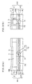
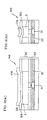
- Fig. 1(a), Fig. 1(b), Fig. 2(a), and Fig. 2(b) are sectional views showing an optical switch according to the present invention.
- Fig. 1(a) is a longitudinal vertical sectional view of a cell 3 of an optical switch 44
- Fig. 1(b) is a transverse vertical sectional view of the cell 3 of the optical switch 44
- Fig. 2(a) and Fig. 2(b) indicate corresponding sectional views in the activated state.
- side walls 6 forming the cell 3 are constituted by piezoelectric/electrostrictive elements or antiferroelectric elements, and an electric field is applied to the piezoelectric/electrostrictive elements or the antiferroelectric elements of the side walls to expand/contract the side walls and thus change the volume of the cell 3, thereby enabling a gas 31 stored in the cell 3 inside a cell member 2 to be ejected from a communicating hole 73 into a fine slit 13.
- an optical waveguide is constituted in such a way that it intersects the gas 31 in the fine slit 13 at a portion of the ejected gas, and at such a intersection area, optical transmission channels can be switched over each time the fine slit 13 is filled with either a liquid 32 or a gas 31.
- the refractive index of the liquid 32 stored in fine slit 13 intersecting the optical waveguide is adjusted so as to be substantially the same as that in the optical waveguide.
- An optical cell 44 is constructed by the cell member 2 formed inside the cell 3 and a waveguide member 42 having the fine slit 13.
- the side walls of the cell 3 are formed from piezoelectric/electrostrictive elements or antiferroelectric elements, and the cell 3 is filled with the gas 31.
- the fine slit 13 is filled with a liquid 32 into which the gas cannot be dissolved.
- both the cell 3 in the cell member 2 and the fine slit 13 in the waveguide member 42 are communicated to each other via a communicating hole 73 to which a communicating opening 72 of the cell member 2 and a nozzle 8 of the waveguide member 42 are both communicated.
- a communicating hole 73 to which a communicating opening 72 of the cell member 2 and a nozzle 8 of the waveguide member 42 are both communicated.
- the communicating opening 72 of the cell member 2 is designed to be greater than the nozzle 8 of the waveguide member 42, since the ceramic materials such as piezoelectric/electrostrictive material or antiferroelectric material provide a considerable difference in shrinkage in the firing phase, thereby inducing a possible positional shift in the location of the communicating opening 72, although it is desirable that as a material for a communicating plate 68 having the communicating opening 72, the same piezoelectric/electrostrictive material or the same antiferroelectric material as the space plate 70 be used.
- the nozzle 8 communicated to the connection opening 72 be machined with high precision, so that the above-mentioned intersection area can be accurately specified by means of the nozzle 8, even if a possible positional error arises in the communicating opening 72.
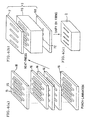
- the cell member 2 can be constituted, for instance, by a spacer plate 70 consisting of piezoelectric/electrostrictive material or antiferroelectric material, said spacer plate forming a plurality of slits (A) 5, a cover plate 7 placing on one side of the spacer plate 70 to cover the slits (A) 5, and a communicating plate 68 placed on the other side of the spacer plate 70 to cover the slits (A) 5. Furthermore, both slits (B) 45 passing through both the cover plate 7 and the spacer plate 70 are formed between the respective specific slit (A) 5 and the adjacent slits (A) 5 of the cell member 2.
- the cell 3 is formed by the slits (A) 5 and the cover plate 7, and each slit (B) 45 separate two adjacent cells 3 from each other.
- each volume-changeable cell 3 is formed so as to be separated from the adjacent cells 3 by the slits (B) 45, hence enabling each cell 3 to be driven completely independently of the other cells 3.
- the adjacent cells 3 can simultaneously perform the same action.
- the piezoelectric/electrostrictive elements or antiferroelectric elements are not mutually disturbed with respect to their displacement. As a result, a smaller field strength is required to obtain, for instance, the same amount of displacement.
- the slit (B) 45 can be formed between the adjacent cells 3 so as not to disturb the deformation of the side walls 6, i.e., the driving parts.
- the slit (B) 45 can be formed in such a manner that it has at least the same length as the deformed part of the cover plate 7 in the axial direction of the cell 3. More preferably the slit (B) 45 can be formed in such a manner that it has the same length as that of the cell 3.
- the novelty resides in the fact that a pressure is not produced by the bending of the walls forming the cell, but the side walls 6 are expanded/contracted in the up/down direction by applying a voltage to electrode layers which are formed, for example, on both surfaces of the side walls 6 forming the cell 3.
- the polarization field of the piezoelectric/electrostrictive elements or antiferroelectric elements forming the side walls 6 of the cell 3, i.e., the driving parts is aligned in the same direction as the driving electric field.
- the state of polarization does not change even if the cells can be driven with a higher field strength. Rather, a more preferable state of polarization can be obtained, and an increased magnitude of strain can stably be obtained. As a result, the cells become more compact, and this is favorable to the optical switch.
- the degree of profile for the surfaces of the side walls 6 forming the cell 3 be less than approximately 8 ⁇ m, and it is desirable that the unevenness for the surfaces of the side walls 6 forming the cell 3 be less than approximately 10 ⁇ m. Moreover, it is desirable that the surface roughness Rt of the surfaces of the side walls 6 forming the cell 3 be less than approximately 10 ⁇ m.
- the inner wall surfaces of the side walls 6, i.e., the driving parts, forming the cell are smooth, and therefore it is difficult for either the concentration of field or the concentration of stress to occur in the activated state. Thus, stable ejection of the gas in the cell can be realized.
- the degree of profile for a surface is defined in Japanese Industrial Standard B0621: "The definition and representation of geometrical deviations".
- the profile of a surface is a surface which is specified so as to have a functionally predetermined shape, and the degree of profile for a surface is the deviation of the surface profile from the geometrical contour, which is determined to theoretically precise dimensions.
- the surfaces of a cell in the present invention mean the cell inner wall surfaces of the side walls forming the above-mentioned cell.
- the ratio of the inside width W (the width in the transverse direction) to the height H of the cell 3, in other words, the aspect ratio W:H of the cell 3, is substantially from 1:2 to 1:40, and it is desirable that the inside width W of the cell 3 be less than approximately 60 ⁇ m (the inside width W and the height H are indicated in Figs. 1(a) and (b)). More preferably, the aspect ratio W:H of the cell 3 should be from 1:10 to 1:25 and the inside width of the cell 3 should be less than 50 ⁇ m.
- An optical switch fulfilling at least one of the above-mentioned conditions, more preferably an optical switch fulfilling both conditions, that is, an optical switch having a greater height and smaller thickness has a compact shape and ensures the operation of the optical switch with a low voltage and a less consumptive electric power.
- Figs. 10(a) to (c) are drawings showing an embodiment of the optical switch according to the present invention, as well as sectional views of parts of a cell member.
- Fig. 10(a) is a longitudinal vertical sectional view of a cell 3 in the optical switch
- Fig. 10(b) is a transverse vertical sectional view of the cell 3 in the optical switch
- Fig. 10(c) is a horizontal sectional view of a spacer plate 70 which forms a cell member 2 of the optical switch.
- a cell 3 having a substantially rectangular shape is effective.
- slit apertures 25 which will become the slits (A) 5 after lamination and slit apertures 15 which will become the slits (B) 45 after lamination are diecut in a green sheet 16 made of the piezoelectric/electrostrictive material or antiferroelectric material, and at the same time the lamination of such a green sheet 16 is carried out with a simultaneous punching/laminating procedure which will be later described, in which case, the lamination is completed just after punching.
- the manufacturing method includes a step for forming piezoelectric/electrostrictive elements or antiferroelectric elements having a predetermined thickness.
- a spacer plate 70 in which the desired slits (A) 5 and the desired slits (B) 45 are both formed, is provided after firing and unifying, and then electrodes are formed in the slits (A) 5 which will become cells.
- the cover plate 7 and the connection plate 68 are joined to the spacer plate 70.
- the green sheets 16 can be formed with a conventional means for producing tapes such as a doctor blade method.
- the cover plate 7 can be formed by a green sheet made of the same material, and the cover plate 7 can be laminated together with the spacer plate 70 and the connection plate 68, and then fired/unified.
- the cover plate 7 and the spacer plate 70 including the driving parts are simultaneously fired to become one ceramic body, thereby enhancing both the sealing durability and the rigidity of the cell.
- an optical switch having a higher response speed can be provided.
- the formation of electrodes is carried out by applying a paste for electrodes onto soft green sheets. In this step, however, precautions must be taken so as not to break or deform the green sheets.
- the cell member 2 inside which the cells are formed is produced, and then electrodes are formed on the surfaces of the side walls of the cells 3 in the cell member 2, though this is not shown. After that, wiring to the electrodes is carried out to activate the cells, and a waveguide member 42 having the fine slit 13 and optical waveguides at predetermined positions is joined to (see Figs. 1(a) and (b)).
- a less dissolvable gas 31 such as argon
- the cells 3 are communicated to the outside only via communicating holes 73 communicated to the fine slits 13, and further, the less dissolvable gas 31 exists in the cells 3, so that the liquid 32 cannot reach either the inside of the cell 3 or interfaces between the liquid, and the gas is formed in the communicating holes 73.
- the side walls 6 of the cell 3 are expanded/contracted with the aid of predetermined signals, and then the volume of the cells 3 can be decreased.
- such an optical switch can be realized by projecting the interfaces into the corresponding intersection areas of the optical waveguides in the fine slits 13.
- Figs. 6(a) to (e) show an actual method for performing the above-mentioned simultaneous punching/laminating procedure.
- a die assembly consisting of a punch 10 and a die 12 is used, wherein a stripper 11 used to laminate the green sheets 16 (hereafter simply referred to as sheets) is disposed around the sheets.
- Fig. 6(a) shows the initial state in which a first sheet 16a is laid on the die 12 and the punching is not yet performed, and in Fig. 6(b), the punch 10 and the stripper 11 are lowered, and then the sheet 16 is punched to form slits (first substep).
- a second sheet 16b is prepared for punching.
- the first sheet 16a is moved upwards, while maintaining it in tight contact with the stripper 11, and the sheet 16a is removed from the die 12 (second substep).
- the method of bringing the sheet 16 into tight contact with the stripper 11 can be realized, for instance, by evacuating air through suction holes disposed in the stripper 11.
- the punch 10 and the stripper 11 are moved upwards from the die 12.
- the front end of the punch 10 does not return into the slit apertures of the first sheet 16a which is raised together therewith, and it is important to stop the front end at a position withdrawn slightly from the lowest part of the first sheet 16a when it stops (third substep).
- the punch 10 is returned into the apertures of the first sheet 16a or when it is completely inserted into the stripper 11, the apertures thus formed are deformed due to the softness of the sheet 16, so that the flatness of the side surfaces of the slit is deteriorated in the process of forming the slits by laminating the sheets 16.
- Fig. 6(d) shows the process of punching the second sheet 16b.
- the second sheet 16b can easily be placed on the die 12, and it can be punched with a procedure similar to that in Fig. 6(b), and at the same time the second sheet can be placed on the first sheet 16a (fourth substep).
- the punched second sheet 16b is placed on the first sheet 16a, and then the sheets are moved upwards with the stripper 11 (fifth substep), thus being prepared for punching a third sheet 16c.
- a predetermined number of the laminated sheets 16 are further repeatedly punched and laminated.
- Fig. 6(e) shows a state in which the punching has been completed.
- the sheets 16 held by the stripper 11 are released, thereby allowing the punched and laminated sheets 16 to removed from the stripper 11.
- Removing the sheets from the stripper 11 can be securely performed by applying a removing tool 17 to the lowest surface of the stripper 11, as shown in the drawings.
- the slit apertures are formed in the respective green sheets and, at the same time, the green sheets thus punched are laminated.
- the punch itself is used as an axis for adjusting the position of lamination in the punching process, the slit apertures formed by the punching are prevented from being deformated, so that the deformation of the slit apertures can be suppressed.
- the positional deviation between the green sheets thus laminated can be maintained to be within less than 5 ⁇ m, thereby enabling the lamination of the green sheets to be carried out with high precision and, at the same time, making it possible to form very smooth side walls for the slits.
- the slit width is approximately several tens of ⁇ m and/or even if the slits have an a high aspect ratio as high as 10 to 25, such slits forming the cells in the subsequent process and the slits between the cells are formed with ease, thereby allowing an optical switch having excellent properties to be provided.
- the slit width which is substantially the same as the width of the punching die during punching of the sheets, is decreased after firing.
- the combination of the procedure of machining thin slits and shrinkage of the dimensions during firing makes it possible to form very fine slits whose width is less than 40 ⁇ m.
- slits other than straight ones can be easily formed in accordance with the design of a punching die assembly, for example, by changing the shape of the die, and therefore an optimal slit shape can be provided in accordance with the application concerned.
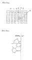
- Fig. 5(a) shows the end surface of the spacer plate 70 shown in Fig. 3(b) after firing, viewed from P, in which case, the spacer plate 70 is produced with the simultaneous punching/laminating procedure shown in Figs. 6(a) to (e).
- Fig. 5(b) schematically shows a magnified section of part M of the wall surfaces of a slit in Fig. 5(a).
- the slits are formed before firing, as described above, and therefore the side wall surfaces which may later form the cells are formed by the fired surfaces.
- the crystal grains with transgranular fractures are less than 1%, which means substantially zero, thereby causing no deterioration of the properties resulting from residual compressive stress, and making it possible to enhance both the durability and the reliability.
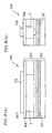
- Fig. 8(a), Fig. 8(b), Fig. 9(a), and Fig. 9(b) are sectional views of this embodiment of the optical switch according to the present invention.
- Fig. 8(a) is a longitudinal sectional view of a cell 3 in the optical switch 144
- Fig. 8(b) is a transverse sectional view of the cell 3 in the optical switch 144.
- Figs. 9(a) and (b) show corresponding activated states.
- Figs. 7(a) and 7(b) show sectional views of a cell member 102 in an optical switch 144. That is, Fig. 7(a) is a longitudinal vertical sectional view of a cell in the optical switch 144, and Fig. 7(b) is a horizontal sectional view viewed from AA in Fig. 7(a).
- the optical switch 144 as another embodiment of an optical switch according to the present invention has a thin vibration plate 166 as a component of the cell member 102.
- the optical switch 144 is formed, for instance, by laminating green sheets and by simultaneously firing and unifying them, and finally by forming on the outer surface of the vibration plate 166 piezoelectric/electrostrictive elements 179 (or antiferroelectric elements) consisting of a piezoelectric/electrostrictive film 178 (or an antiferroelectric film) including at least one pair of electrode films 173 and 177.
- the optical switch 144 is different from the optical switch 44 in Figs. 2(a) and (b) regarding the following point:
- the ejection/suction of the gas 31 from/towards the cell 3 is carried out not by the expansion/constriction of side walls 6 of the cell 3, but by decompression/compression of the cell 3 due to the bending vibration of the vibration plate 166.
- the optical switch 144 In comparison with the optical switch 44 which is operated based on the vibration of expansion/contraction of the side walls 6 in the cells 3, the optical switch 144 has the following advantages and disadvantages.
- the cells 3 in the optical switch 144 be arranged in a matrix form, and therefore it is preferable that, for instance, the method for manufacturing an actuator which is used in such a display unit, as disclosed in Japanese Unexamined Patent Application Publication No. 10-78549, be employed.
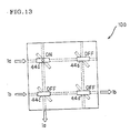
- Figs. 11 to 13 show horizontal sectional views of the optical switch according to the present invention for explaining the function in the application.
- a waveguide switch 100 optical waveguides C1, C2, R1 and R2 are arranged in a checkerboard form on a substrate made of, e.g., silica, and optical switches 44a - 44d are disposed at the intersection areas of the waveguides.
- Fig. 11 shows a horizontal sectional view of the optical switch at the level of the fine slits 13
- Fig. 12 and Fig. 13 show horizontal sectional views of the optical switch at the level of the cells 3.
- light signals 1a and 1b are respectively supplied from the optical waveguide R1 (left side in the drawing) and the optical waveguide R2 (left side in the drawing), as shown in Fig. 11.
- the light signals 1a and 1b travel in the waveguides R1 and R2, respectively.
- the switch 44a is turned on, i.e., in the ON state, as shown in Fig. 13
- the light signal 1b travels in the optical waveguide R2
- the light signal 1a is deflected, for instance, towards the right side at the optical switch 44a, and then conducted into the optical waveguide Cl.
- the light signal 1a travels in the optical waveguide C1, because the optical switch 44c is in the OFF state.
- a ceramic material including one or more of, for instance, lead zirconate, lead magnesium niobate, lead nickel niobate, lead zinc niobate, lead manganese niobate, lead antimony stannate, lead titanate, barium titanate, lead magnesium tungstate, lead cobalt niobate, and the like can be used. It is desirable that these ceramic materials are as a main component of more than 50 wt% in the piezoelectric/electrostrictive elements. In particular, it is preferable that the ceramic material includes lead zirconate.
- the ceramic material furthermore, one or more of lanthanum oxide, calcium oxide, strontium oxide, molybdenum oxide, tungsten oxide, barium oxide, niobium oxide, zinc oxide, nickel oxide, manganese oxide, and the like can be included.
- the ceramic material has a main component consisting of lead magnesium niobate, lead zirconate, and lead titanate, and at least one of lanthanum and strontium is included therein.
- a ceramic material having lead zirconate as a main component, a ceramic material having lead zirconate and lead stannate as main components, a ceramic material having lead zirconate as a main component, in which a lanthanum oxide is doped, or a ceramic material having lead zirconate and lead stannate as main components in which lead zirconate or lead niobate is doped can preferably be used.
- barium titanate As another material for the piezoelectric/electrostrictive elements, moreover, barium titanate, a ceramic ferroelectric material of a titanium/barium system having barium titanate as a main component, a polymer piezoelectric material such as polyvinylidene fluoride (PVDF), or a ceramic piezoelectric material of the Bi system such as (Bi 0.5 Na 0.5 ) TiO 3 , and a ceramic material of a Bi layer can be used.
- PVDF polyvinylidene fluoride
- Bi Bi 0.5 Na 0.5
- Bi layer As another material for the piezoelectric/electrostrictive elements, moreover, barium titanate, a ceramic ferroelectric material of a titanium/barium system having barium titanate as a main component, a polymer piezoelectric material such as polyvinylidene fluoride (PVDF), or a ceramic piezoelectric material of the Bi system such as (Bi 0.5 Na 0.5 ) TiO
- a mixture and a solid solution of the above-mentioned materials having an improved piezoelectric/electrostrictive property, or a material produced by the above-mentioned material, or a mixture of the above-mentioned materials into which doping materials are added can also be used.
- the present invention has solved the problems in the conventional art.
- the optical switching has been realized not by generating bubbles with micro heaters as in the conventional art, but by the movement of bubbles at room temperature with the aid of micro pumps, so that the power loss in the optical switch is suppressed even if the response speed is increased.
- the optical switch according to the present invention provides a reduced manufacturing cost, excellent durability, and smaller power consumption. Since, moreover, the disposable liquid in the conventional art is not employed, no supporting mechanism for collecting and recycling the liquid is required, hence making it easy to reduce the manufacturing cost and to miniaturize the overall system.
Landscapes
- Engineering & Computer Science (AREA)
- Manufacturing & Machinery (AREA)
- Physics & Mathematics (AREA)
- General Physics & Mathematics (AREA)
- Optics & Photonics (AREA)
- Mechanical Engineering (AREA)
- General Engineering & Computer Science (AREA)
- Mechanical Light Control Or Optical Switches (AREA)
Abstract
Description
Claims (4)
- An optical switch being disposed in intermediate positions of optical paths to define a channel of a light signal, characterized in that
said optical switch is constituted of a cell member in whose interior cells are formed, and a waveguide member having fine slits, a gas is filled in said cells of which side walls are formed by piezoelectric/electrostrictive elements or antiferroelectric elements, and a liquid is filled in the fine slits, the cells and the fine slits being communicated to each other via a communicating hole,
optical waveguides intersect at the fine slits, and the cells are disposed at the crossing locations, and
said side walls are expanded/constricted by applying an electric field to the piezoelectric/electrostrictive elements or antiferroelectric elements which form the side walls of the cells, and a part of the gas stored in each cell is ejected at a corresponding intersection area from said communicating hole into the corresponding fine slit. - An optical switch according to claim 1, wherein the polarization field of said piezoelectric/electrostrictive elements or antiferroelectric elements is aligned in the same direction as the driving electric field.
- An optical switch according to claim 1, wherein regarding the state of crystal grains in the surfaces of the side walls forming said cell, the crystal grains suffering transgranular fracture are less than 1%.
- A method for manufacturing with a punch and die an optical switch which consists of a cell member inside which cells are formed and a waveguide member having fine slits, wherein said cells, whose side walls are formed by piezoelectric/electrostrictive elements or antiferroelectric elements, are filled with a gas, and said fine slits are filled with a liquid, said cells and said fine slits being communicated to each other via a corresponding communicating hole, wherein optical waveguides are intersected at said fine slits, and said cells are disposed at the intersection areas, characterized in that said method comprises the steps of:preparing a plurality of green sheets made of piezoelectric/electrostrictive material or antiferroelectric material;performing a first substep for machining first slit apertures in a first green sheet with said punch, a second substep for raising said first green sheet in tight contact with a stripper in the state where said punch is not withdrawn from said first slit apertures, and a third substep for raising said punch in such a manner that the front end of said punch is withdrawn slightly from the lowest part of said first green sheet thus raised;performing a fourth substep for machining second slit apertures in a second green sheet with said punch, a fifth substep for raising said second green sheet together with said first green sheet in the state where said punch is not withdrawn from said second slit apertures, and a sixth substep for raising said punch in such a manner that the front end of said punch is withdrawn slightly from said second green sheet thus raised; andsubsequently laminating a plurality of green sheets by repeating the fourth substep to the sixth substep, and then forming the piezoelectric/electrostrictive elements or antiferroelectric elements including a plurality of slits.
Applications Claiming Priority (7)
| Application Number | Priority Date | Filing Date | Title |
|---|---|---|---|
| JP2001108986 | 2001-04-06 | ||
| JP2001108986 | 2001-04-06 | ||
| JP2001189718 | 2001-06-22 | ||
| JP2001189718 | 2001-06-22 | ||
| US09/915,234 US6507682B2 (en) | 2001-04-06 | 2001-07-25 | Optical switch |
| US915234 | 2001-07-25 | ||
| PCT/JP2002/003437 WO2002084373A1 (en) | 2001-04-06 | 2002-04-05 | Optical switch |
Publications (3)
| Publication Number | Publication Date |
|---|---|
| EP1376190A1 true EP1376190A1 (en) | 2004-01-02 |
| EP1376190A4 EP1376190A4 (en) | 2007-03-14 |
| EP1376190B1 EP1376190B1 (en) | 2009-01-07 |
Family
ID=27346485
Family Applications (1)
| Application Number | Title | Priority Date | Filing Date |
|---|---|---|---|
| EP02714494A Expired - Lifetime EP1376190B1 (en) | 2001-04-06 | 2002-04-05 | Optical switch |
Country Status (3)
| Country | Link |
|---|---|
| US (2) | US6507682B2 (en) |
| EP (1) | EP1376190B1 (en) |
| WO (1) | WO2002084373A1 (en) |
Cited By (1)
| Publication number | Priority date | Publication date | Assignee | Title |
|---|---|---|---|---|
| CN101799573B (en) * | 2009-10-13 | 2011-09-07 | 南京邮电大学 | Two dimension electro-optical switch array device based on microfluidic technology |
Families Citing this family (12)
| Publication number | Priority date | Publication date | Assignee | Title |
|---|---|---|---|---|
| EP0907212A1 (en) * | 1996-11-29 | 1999-04-07 | Ngk Insulators, Ltd. | Ceramic element, method of manufacturing ceramic element, display, relay device, and capacitor |
| FI108204B (en) * | 1999-11-25 | 2001-11-30 | Kari Johannes Kirjavainen | Film for transforming energy |
| US6699018B2 (en) * | 2001-04-06 | 2004-03-02 | Ngk Insulators, Ltd. | Cell driving type micropump member and method for manufacturing the same |
| US6507682B2 (en) * | 2001-04-06 | 2003-01-14 | Ngk Insulators, Ltd. | Optical switch |
| JP3973458B2 (en) * | 2002-03-15 | 2007-09-12 | 三菱電機株式会社 | Light switch |
| US6718085B1 (en) * | 2002-10-07 | 2004-04-06 | Agilent Technologies, Inc. | Stable optical switch with reduced power consumption |
| US20040076363A1 (en) * | 2002-10-16 | 2004-04-22 | Schroeder Dale W. | Optical switch with increased operational stability |
| JP4842520B2 (en) * | 2003-05-30 | 2011-12-21 | 日本碍子株式会社 | Cell driving type piezoelectric / electrostrictive actuator and manufacturing method thereof |
| US7447397B1 (en) | 2004-06-14 | 2008-11-04 | Dynamic Method Enterprises Limited | Optical switch matrix |
| US20220128760A1 (en) * | 2019-01-18 | 2022-04-28 | Commscope Technologies Llc | Optical waveguide switch and method of making same |
| US11430813B2 (en) | 2019-08-15 | 2022-08-30 | Sandisk Technologies Llc | Antiferroelectric memory devices and methods of making the same |
| US11502104B2 (en) | 2019-08-15 | 2022-11-15 | Sandisk Technologies Llc | Antiferroelectric memory devices and methods of making the same |
Family Cites Families (11)
| Publication number | Priority date | Publication date | Assignee | Title |
|---|---|---|---|---|
| FR2418539A1 (en) * | 1978-02-24 | 1979-09-21 | Orega Circuits & Commutation | Liquid contact relays driven by piezoelectric membrane - pref. of polyvinylidene fluoride film for high sensitivity at low power |
| US4245886A (en) * | 1979-09-10 | 1981-01-20 | International Business Machines Corporation | Fiber optics light switch |
| JPH05289006A (en) * | 1992-04-13 | 1993-11-05 | Fujikura Ltd | Optical path switching device |
| US5650810A (en) * | 1992-12-03 | 1997-07-22 | Brother Kogyo Kabushiki Kaisha | Ink jet print head having a manifold wall portion and method of producing the same by injection molding |
| DE19527566A1 (en) * | 1995-07-27 | 1997-01-30 | Sel Alcatel Ag | Optical changeover switch - has channels at light conductor crossings on substrate connected to reservoir containers, one contg. medium with same refractive index as light conductor core, the other a medium with lower refractive index |
| US5699462A (en) * | 1996-06-14 | 1997-12-16 | Hewlett-Packard Company | Total internal reflection optical switches employing thermal activation |
| DE19711564C2 (en) * | 1997-03-20 | 1999-07-08 | Inst Mikrotechnik Mainz Gmbh | Optical switching element and switching arrangement |
| DE19711559C2 (en) * | 1997-03-20 | 2000-11-02 | Inst Mikrotechnik Mainz Gmbh | Optical multiple switch |
| JP3537700B2 (en) * | 1998-09-29 | 2004-06-14 | 京セラ株式会社 | Printing equipment |
| JP3077758B1 (en) * | 1999-05-11 | 2000-08-14 | 日本電信電話株式会社 | Light switch |
| US6507682B2 (en) * | 2001-04-06 | 2003-01-14 | Ngk Insulators, Ltd. | Optical switch |
-
2001
- 2001-07-25 US US09/915,234 patent/US6507682B2/en not_active Expired - Fee Related
-
2002
- 2002-04-05 EP EP02714494A patent/EP1376190B1/en not_active Expired - Lifetime
- 2002-04-05 WO PCT/JP2002/003437 patent/WO2002084373A1/en not_active Ceased
- 2002-10-04 US US10/264,686 patent/US6647169B2/en not_active Expired - Fee Related
Cited By (1)
| Publication number | Priority date | Publication date | Assignee | Title |
|---|---|---|---|---|
| CN101799573B (en) * | 2009-10-13 | 2011-09-07 | 南京邮电大学 | Two dimension electro-optical switch array device based on microfluidic technology |
Also Published As
| Publication number | Publication date |
|---|---|
| EP1376190A4 (en) | 2007-03-14 |
| US6647169B2 (en) | 2003-11-11 |
| US6507682B2 (en) | 2003-01-14 |
| WO2002084373A1 (en) | 2002-10-24 |
| US20020168132A1 (en) | 2002-11-14 |
| US20030041457A1 (en) | 2003-03-06 |
| EP1376190B1 (en) | 2009-01-07 |
Similar Documents
| Publication | Publication Date | Title |
|---|---|---|
| EP1376190B1 (en) | Optical switch | |
| US7861388B2 (en) | Method of manufacturing a cell driving type piezoelectric/electrostrictive actuator | |
| US6752601B2 (en) | Micropump | |
| US6988301B2 (en) | Method for manufacturing a matrix type actuator | |
| US20040201324A1 (en) | Matrix type piezoelectric/electrostrictive device and manufacturing method thereof | |
| US7161281B2 (en) | Less-dust-generative piezoelectric/electrostrictive device and manufacturing method | |
| KR101153613B1 (en) | Micro-ejector and method for manufacturing the same | |
| JP3964193B2 (en) | Matrix type actuator | |
| EP1432048A1 (en) | MATRIX TYPE PIEZOELECTRIC/ELECTROSTRICTIVE DEVICE AND ITS MANUFACTURING METHOD | |
| JP4723199B2 (en) | Cylindrical piezoelectric actuator, cylindrical piezoelectric actuator array, and manufacturing method | |
| US7374628B2 (en) | Method for manufacturing a cell-driving-type micro pump member | |
| JP3749676B2 (en) | Light switch | |
| US20020140318A1 (en) | Matrix type actuator | |
| JP5139672B2 (en) | Multilayer piezoelectric element and method for manufacturing the same | |
| EP1263059B1 (en) | Matrix actuator | |
| JP2005019949A (en) | Cell driving piezoelectric/electrostrictiv actuator and its fabricating process | |
| US20040119791A1 (en) | Multislit type actuator, inkjet head and method for manufacturing multislit type actuator | |
| JP2007335485A (en) | Multilayer piezoelectric actuator and manufacturing method thereof |
Legal Events
| Date | Code | Title | Description |
|---|---|---|---|
| PUAI | Public reference made under article 153(3) epc to a published international application that has entered the european phase |
Free format text: ORIGINAL CODE: 0009012 |
|
| 17P | Request for examination filed |
Effective date: 20030822 |
|
| AK | Designated contracting states |
Kind code of ref document: A1 Designated state(s): AT BE CH CY DE DK ES FI FR GB GR IE IT LI LU MC NL PT SE TR |
|
| AX | Request for extension of the european patent |
Extension state: AL LT LV MK RO SI |
|
| A4 | Supplementary search report drawn up and despatched |
Effective date: 20070214 |
|
| RIC1 | Information provided on ipc code assigned before grant |
Ipc: G02B 6/35 20060101AFI20070208BHEP |
|
| 17Q | First examination report despatched |
Effective date: 20070619 |
|
| GRAP | Despatch of communication of intention to grant a patent |
Free format text: ORIGINAL CODE: EPIDOSNIGR1 |
|
| GRAS | Grant fee paid |
Free format text: ORIGINAL CODE: EPIDOSNIGR3 |
|
| GRAA | (expected) grant |
Free format text: ORIGINAL CODE: 0009210 |
|
| AK | Designated contracting states |
Kind code of ref document: B1 Designated state(s): DE FR GB |
|
| REG | Reference to a national code |
Ref country code: GB Ref legal event code: FG4D |
|
| REF | Corresponds to: |
Ref document number: 60230730 Country of ref document: DE Date of ref document: 20090226 Kind code of ref document: P |
|
| PLBE | No opposition filed within time limit |
Free format text: ORIGINAL CODE: 0009261 |
|
| STAA | Information on the status of an ep patent application or granted ep patent |
Free format text: STATUS: NO OPPOSITION FILED WITHIN TIME LIMIT |
|
| 26N | No opposition filed |
Effective date: 20091008 |
|
| REG | Reference to a national code |
Ref country code: FR Ref legal event code: ST Effective date: 20091231 |
|
| PG25 | Lapsed in a contracting state [announced via postgrant information from national office to epo] |
Ref country code: DE Free format text: LAPSE BECAUSE OF NON-PAYMENT OF DUE FEES Effective date: 20091103 |
|
| PG25 | Lapsed in a contracting state [announced via postgrant information from national office to epo] |
Ref country code: FR Free format text: LAPSE BECAUSE OF NON-PAYMENT OF DUE FEES Effective date: 20091222 |
|
| PGFP | Annual fee paid to national office [announced via postgrant information from national office to epo] |
Ref country code: GB Payment date: 20120327 Year of fee payment: 11 |
|
| GBPC | Gb: european patent ceased through non-payment of renewal fee |
Effective date: 20130405 |
|
| PG25 | Lapsed in a contracting state [announced via postgrant information from national office to epo] |
Ref country code: GB Free format text: LAPSE BECAUSE OF NON-PAYMENT OF DUE FEES Effective date: 20130405 |