EP1372268A2 - A reference ladder having improved feedback stability - Google Patents
A reference ladder having improved feedback stability Download PDFInfo
- Publication number
- EP1372268A2 EP1372268A2 EP03013658A EP03013658A EP1372268A2 EP 1372268 A2 EP1372268 A2 EP 1372268A2 EP 03013658 A EP03013658 A EP 03013658A EP 03013658 A EP03013658 A EP 03013658A EP 1372268 A2 EP1372268 A2 EP 1372268A2
- Authority
- EP
- European Patent Office
- Prior art keywords
- tap
- ladder
- taps
- voltage
- current source
- Prior art date
- Legal status (The legal status is an assumption and is not a legal conclusion. Google has not performed a legal analysis and makes no representation as to the accuracy of the status listed.)
- Granted
Links
Images



Classifications
-
- H—ELECTRICITY
- H03—ELECTRONIC CIRCUITRY
- H03M—CODING; DECODING; CODE CONVERSION IN GENERAL
- H03M1/00—Analogue/digital conversion; Digital/analogue conversion
- H03M1/06—Continuously compensating for, or preventing, undesired influence of physical parameters
- H03M1/0602—Continuously compensating for, or preventing, undesired influence of physical parameters of deviations from the desired transfer characteristic
-
- H—ELECTRICITY
- H03—ELECTRONIC CIRCUITRY
- H03M—CODING; DECODING; CODE CONVERSION IN GENERAL
- H03M1/00—Analogue/digital conversion; Digital/analogue conversion
- H03M1/12—Analogue/digital converters
- H03M1/34—Analogue value compared with reference values
- H03M1/36—Analogue value compared with reference values simultaneously only, i.e. parallel type
- H03M1/361—Analogue value compared with reference values simultaneously only, i.e. parallel type having a separate comparator and reference value for each quantisation level, i.e. full flash converter type
- H03M1/362—Analogue value compared with reference values simultaneously only, i.e. parallel type having a separate comparator and reference value for each quantisation level, i.e. full flash converter type the reference values being generated by a resistive voltage divider
- H03M1/365—Analogue value compared with reference values simultaneously only, i.e. parallel type having a separate comparator and reference value for each quantisation level, i.e. full flash converter type the reference values being generated by a resistive voltage divider the voltage divider being a single resistor string
Definitions
- the present invention generally relates to a reference ladder having improved feedback stability that can provide reference voltages for an analog-to-digital converters (ADC), and other types of circuits that utilize reference voltages.
- ADC analog-to-digital converters
- ADCs Analog-to-digital converters
- ADCs convert analog signals into a digital format for further efficient processing using digital circuits and/or processors.
- digital control and processing are applied to more numerous applications, the demand for ADCs continues to increase.
- ADCs that are inexpensive and that provide high performance.
- a conventional ADC often includes a voltage reference ladder (also called a reference ladder) having a resistor ladder with a plurality of taps. Each tap provides a reference voltage that is utilized by the ADC to quantize the incoming analog signal. More specifically, a bank of ADC comparators (or differential input stages) compares the reference voltages from the reference ladder to the analog signal in order to quantize the analog signal and generate a digital output signal.
- a voltage reference ladder also called a reference ladder
- ADC comparators or differential input stages
- the accuracy of the analog-to-digital conversion is heavily dependent on the accuracy of the reference voltages from the reference ladder. More specifically, the ADC full scale range is controlled by these voltages. Accordingly, a feedback network is utilized to maintain the accuracy of the reference voltages.
- the feedback network utilizes certain taps of the reference ladder known conventionally as "sense" points or taps, and "force" points (or taps).
- a voltage or current source is applied at the force taps to control the reference voltages that are produced by the reference ladder.
- the force taps are usually the first and last taps on the reference ladder.
- the sense taps are certain taps on the reference ladder that are monitored (or sensed) to check if the desired reference voltages are being produced by the reference ladder. More specifically, an operational amplifier (op amp) compares the voltage across the sense taps with a desired reference voltage (e.g. ADC full scale voltage), and adjusts the voltage or current source at the force taps to produce the desired voltage across the sense taps.
- a desired reference voltage
- a bank of ADC comparators are connected to the taps of the reference ladder and receive the reference voltages.
- the ADC comparators have associated circuit parasitics that load the sense taps.
- the parasitics of the ADC comparators effect the voltage and current at the sense taps, and effectively load the feedback control loop that drives the force taps of the reference ladder.
- the sense taps are taken across a subset of the plurality of taps, a portion of the reference ladder resistance is also in the feedback control loop. Both the circuit parasitcs and the reference ladder resistance contribute to destabilization of the feedback control loop.
- the reference ladder so as to prevent the ADC comparators and the ladder resistance from loading the feedback control loop, so as to improve the loop stability.
- the present invention is a voltage reference ladder that has improved feedback stability.
- the voltage reference ladder includes a resistor ladder having a plurality of taps to produce a plurality of output voltages that can be used as reference voltages by an ADC, or another type of circuit.
- the resistor ladder is driven by a first current source at a first tap of the plurality of taps and by a second current source at a second tap of the plurality of taps.
- a first feedback network senses a voltage at the first tap and controls the first current source based on the first sensed voltage.
- a second feedback network senses a voltage at the second tap and controls the second current source based on the second sensed voltage.
- the first and second taps are at opposite ends of the resistor ladder.
- the first and second taps each operate as both a force tap and a sense tap of the resistor ladder. This occurs because the first and second taps are connected to the outputs of their respective current sources, and are also sensed by their respective feedback networks.
- the first feedback network includes a first op amp having a first input connected to the first tap and an output controlling the first current source.
- the second feedback network includes a second op amp having a first input connected to the second tap and an output controlling the second current source.
- the reference voltage is applied across a second input of first op amp and a second input of the second op amp, and is determined by scaling-up the ADC full scale range from V ref to V ref '
- a plurality of differential input stages can be connected to corresponding taps of the resistor ladder to receive the plurality of output voltages from the reference ladder.
- the differential input stages are at least partially isolated from the first feedback network and the second feedback network, thereby improving stability of the first feedback network and the second feedback network when compared to conventional configurations.
- the resistor ladder includes a first resistor ladder and a second resistor ladder, each having a plurality of taps.
- the first resistor ladder is driven by a first current source and a second current source at respective force taps that are located at opposite ends of the first resistor ladder.
- a second resistor ladder is driven by a third current source and a fourth current source at respective force taps that are located at opposite ends of the second resistor ladder.
- the first and second resistor ladders are configured to generate substantially identical output voltages across their respective taps.
- a first feedback network senses a voltage at a first sense tap of the first resistor ladder, and controls both the first current source and the third current source based on the sensed voltage.
- a second feedback network senses a voltage at a second sense tap of the first resistor ladder, and controls both the second current source and the fourth current source based on the voltage that is sensed at the second sense tap.
- the first and second feedback networks control the respective current sources of both of the first and second resistor ladders, but only sense voltage from the first resistor ladder.
- a plurality of differential input stages receive the plurality of voltages from the second resistor ladder.
- the plurality of differential input stages are at least partially isolated from the feedback networks because the sense taps for the feedback networks are taken from the first resistor ladder, and not the second resistor ladder.
- the conventional reference ladder 100 includes a reference generator 102 that generates a voltage reference V ref , op amps 104 and 106, and a resistor ladder 112.
- the resistor ladder 112 includes multiple resistors 118 that are series-connected, and taps 119 between the resistors 118.
- the resistor ladder 112 is driven by a current source 108 at the top, and by a current source 110 at the bottom of the resistor ladder 112.
- the taps 119 of the resistor ladder (between the resistors 118) provide the reference voltages for the ADC.
- the reference voltages are used by the ADC differential input stages to quantize the analog input. (See Fig. 4)
- the first and last taps 114a and 114b are referred to as force taps, as this is where the current sources 108 and 110 drive the resistor ladder 112.
- the taps 116a and 116b are referred to as sense taps, as the sense taps are used to sense the voltage on the resistor ladder 112.
- the op amp 104, the current source 108, and the sense point 116a form a feedback network 120.
- the op amp 106, the current source 110, and the sense point 116b form a feedback network 122.
- the op amp 104 compares the voltage at the sense tap 116a to the voltage V ref produced by the voltage generator 102, and generates an output based on the difference.
- the output of the op amp 104 controls the current source 108.
- the op amp 106 compares the voltage at the sense tap 116b to the voltage V ref produced by the voltage generator 102, and generates an output that controls the current source 110.
- the feedback networks 120 and 122 drive the current sources 108 and 110 to set a desired voltage between the sense taps 116a and 116b equal to V ref .
- the voltage V ref is set to the "ADC full scale range” so that the feedback networks 120,122 drive the voltage across the sense taps 116 to this voltage.
- the "ADC full scale range” generally represents the voltage that the analog input signal is expected to fall within. Therefore, the taps 119 within the ADC full scale range should provide a sufficient number of reference voltages to quantize the analog input signal. However, additional reference voltages are required to insure linear operation of the ADC, especially at the edges of the "ADC full scale range”.
- various ADC architectures such as folding flash and folding interpolating ADCs, require additional reference voltages that are outside the ADC full scale range.
- the ADC full scale reference voltages can be identified as a first set of reference voltages, and the additional references voltages outside the ADC full scale range can be identified as a second set of reference voltages, to produce a the total voltage drop across the resistor ladder 112.
- the first set of reference voltages and the second additional set of reference voltages are delivered to the ADC differential input stages and are generally known as "ADC reference voltages", shown in FIG. 1.
- the taps 119 are connected to differential input stages (e..g. comparators) that quantize an analog input signal.
- FIG. 4 illustrates the taps 119 connected to a bank of differential input stages 402 that quantize an analog input signal 404 using the reference voltages from the reference ladder 100.
- the differential input stages 402 have parasitics associated with them. These parasitics load the feedback networks 120 and 122 via the taps 119 within the respective feedback networks, causing loop instability. Furthermore, the resistors 118 in the feedback networks 120 and 122 also load the feedback networks and cause instability.
- FIG. 2 illustrates a reference ladder 200 having improved feedback stability according to embodiments of the present invention.
- the reference ladder 200 includes a reference generator 202 that generates a voltage reference V ref ', op amps 104 and 106, and a resistor ladder 204.
- the resistor ladder 204 includes multiple resistors 118 and taps (e.g. 119) between the resistors 118.
- the resistor ladder 204 is driven by the current source 108 at the top and by a current source 110 at the bottom of the resistor ladder 112.
- the taps of the resistor ladder (between the resistors 118) provide the reference voltages for the ADC.
- the "reference voltages" produced by the reference ladder 200 may also be called “output reference voltages" or more generally “output voltages”.
- the op amp 104, the current source 108, and the tap 206a form a feedback network 205.
- the op amp 106, the current source 110, and the tap 206b form a feedback network 208.
- the op amp 104 compares the voltage at the tap 206a to the voltage V ref ' produced by the voltage generator 202, and generates an output based on the difference.
- the output of the op amp 104 controls the current source 108.
- the op amp 106 compares the voltage at the tap 206b to the voltage V ref ' produced by the voltage generator 102, and generates an output that controls the current source 110.
- the feedback networks 205 and 208 drive the current sources 108 and 110 to set a desired voltage between the sense taps 206a and 206b equal to V ref '.
- the current sources 108 and 110 can be configured as voltage sources that produce the necessary current to generate the ADC reference voltages.
- the reference ladder 200 is similar to the reference ladder 100, except that the first tap 206a is connected to the input of the op amp 104, and the last tap 206b is connected to the input of the op amp 106.
- the taps 206a and 206b operate as both force taps and sense taps. Stated another way, the force taps and the sense taps are converged to a single pair of taps 206a and 206b.
- the force taps 114a and 114b are separate and distinct from the sense taps 116a and 116b.
- the reference feedback networks 205 and 208 in the reference ladder 200 are not loaded by any of the resistors 118, or by the differential input stages connected to the taps 119. Therefore, the stability of the feedback networks 205 and 208 is improved.
- the ADC full scale voltage is now a fraction of the voltage across the force/sense taps 206.
- the ADC full scale voltage is equal to voltage across the sense taps 116. Therefore, the voltage V ref ' produced by the voltage generator 202 is a scaled-up version of the voltage V ref that is produce by the voltage generator 102, for a given ADC full scale range.
- the voltage V ref ' is scaled-up to accommodate for the voltage drop across the resistors 118 that are between the force/sense taps 206 and the ADC full scale range, (namely, the first two resistors and the last two resistors in the voltage ladder 204). Whereas, in the reference ladder 100, this voltage drop was considered by the feedback network.
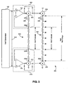
- FIG. 3 illustrates another reference ladder 300 having improved loop stability according to embodiments of the invention.
- Reference ladder 300 includes two resistor ladders to separate the ADC op amps connected to the second resistor ladder from the feedback networks connected to the first resistor ladder. More specifically, reference ladder 300 includes a first resistor ladder 310 having a plurality of resistors 306 with multiple taps in between the resistors that includes sense taps 308a and 308b and force taps 305a and 305b. The sense taps 308a,b are fed back to the respective op amps 104 and 106 for comparison with V ref to form feedback networks 302 and 316.
- the output of the op amp 104 controls a current source 304
- op amp 106 controls a current source 314. Similar to the discussion above, the op amps 104 and 106 control the current sources 304 and 314 so that the voltage across the sense taps 308a and 308b is equal to V ref , which is set to the ADC full scale range.
- the reference ladder 300 also includes a second resistor ladder 324 having a plurality of resistors 322 with multiple taps in between the resistors 322 that generate the ADC reference voltages.
- the second resistor ladder 324 is driven by current sources 318 and 326 at the respective force taps 320a and 320b.
- the second reference ladder does not have any sense taps, as the sensing operation is performed using the first reference ladder.
- the second voltage ladder 324 is configured to produce approximately identical voltages at taps between the resistors 322, as that produced by the corresponding taps of the first voltage ladder 310.
- resistors 322 are selected to have values that are approximately the same as the corresponding resistors 306 in the first resistor ladder 310.
- the current source 318 is the same as the current source 304 and is commonly controlled by the output of the op amp 104.
- the current source 326 is the same as the current source 314 and is commonly controlled by the output of the op amp 106. Accordingly, the reference voltages produced by the reference ladder 324 should match those produced by the resistor ladder 310, where the voltages from the resistor ladder 324 drive the differential input stages in the ADC (e.g. differential input stages 402).
- the differential input stages connected to the taps of the resistor ladder 324 are isolated from the feedback networks 302 and 316. Therefore, the parasitics associated with the ADC differential input stages do not load the feedback network 302 or the feedback network 316, which improves loop stability of these loops.
- the reference ladder discussed herein has been illustrated as part of an ADC. This is done for example purposes only, and is not meant to limit the scope of the invention.
- the reference ladder can be used in other circuit applications besides ADCs, as will be understood by those skilled in the relevant arts.
Landscapes
- Engineering & Computer Science (AREA)
- Theoretical Computer Science (AREA)
- Analogue/Digital Conversion (AREA)
- Amplifiers (AREA)
Abstract
Description
Claims (24)
- A reference ladder, comprising:a resistor ladder having a plurality of taps to produce a plurality of output voltages, and driven by a variable current source at a force tap of the plurality of taps; andan op amp configured to compare a voltage at said force tap to a reference voltage, an output of said op amp controlling said variable current source.
- The reference ladder of claim 1, wherein said force tap is also a sense tap for said resistor ladder.
- The reference ladder of claim 1, wherein said op amp includes a first input and a second input, said reference voltage connected to said first input and said force tap connected to said second input.
- The reference ladder of claim 1, wherein said plurality of taps are coupled to a corresponding plurality of differential input stages that receive said plurality of output voltages from said reference ladder.
- The reference ladder of claim 4, wherein said differential input stages are at least partially isolated from a feedback network formed by said op amp and said variable current source.
- The reference ladder of claim 4, wherein said differential input stages are at least partially isolated from a first input of said op amp.
- The reference ladder of claim 1, wherein said reference voltage is approximately set to a full scale voltage, said full scale voltage sufficient to quantize an analog input signal.
- The reference ladder of claim 7, wherein said full scale voltage is a fraction of a total output voltage taken across a first tap and a last tap of said plurality of taps.
- A reference ladder, comprising:wherein said sense tap is the same as said force tap.a resistor ladder having a plurality of taps to produce a plurality of output voltages, and driven by a variable current source at a force tap of the resistor ladder; anda feedback network sensing a voltage at a sense tap of said plurality of taps, and controlling said variable current source based on said sensed voltage;
- The reference ladder of claim 9, wherein said feedback network includes an op amp having a first input connected to said sense tap and second input connected to said reference voltage, and an output that controls said variable current source.
- The reference ladder of claim 9, further comprising:a second feedback network sensing a voltage at a second sense tap of said plurality of taps and controlling a second variable current source that is connected to a second force tap of the plurality of taps, wherein said second force tap is also said second sense tap.
- A reference ladder, comprising:a resistor ladder having a plurality of taps to produce a plurality of output voltages, said resistor ladder driven by a first current source at a first tap of the plurality of taps and by a second current source at a second tap of the plurality of taps;a first feedback network sensing a voltage at said first tap and controlling said first variable current source based on said first sensed voltage; anda second feedback network sensing a voltage at said second tap and controlling said second variable current source based on said second sensed voltage.
- The reference ladder of claim 12, wherein said first and second taps are at opposite ends of said resistor ladder.
- The reference ladder of claim 12, wherein said first tap operates as both a force tap and a sense tap of said resistor ladder.
- The reference ladder of claim 12, wherein said second tap operates as both a force tap and a sense tap of said resistor ladder.
- The reference ladder of claim 12, wherein:said first feedback network includes a first op amp having a first input connected to said first tap and an output controlling said first current source;said second feedback network includes a second op amp having a first input connected to said second tap and an output controlling said second current source; anda reference voltage applied across a second input of said first op amp and a second input of said second op amp.
- The reference ladder of claim 12, wherein said reference voltage is scaled-up from a full scale range voltage.
- The reference ladder of claim 12, wherein said plurality of taps of said resistor ladder are coupled to a plurality of differential input stages, said differential input stages at least partially isolated from said first feedback network and said second feedback network, thereby improving stability of said first feedback network and said second feedback network.
- A reference ladder, comprising:a first resistor ladder having a first plurality of taps and driven by a first variable current source at a first force tap, one of said plurality of taps being a sense tap;a second resistor ladder having a second plurality of taps and driven by a second variable current source at a second force tap to provide a plurality of output voltages; anda feedback network sensing a voltage at said sense tap of said first resistor ladder, and controlling said first variable current source and said second variable current source based on said voltage that is sensed at said sense tap.
- The reference ladder of claim 19, wherein said sense tap is determined based on a full scale range voltage.
- The reference ladder of claim 19, wherein said plurality of taps of said second resistor ladder are connected to a plurality of differential input stages that receive said plurality of output voltages.
- The reference ladder of claim 21, wherein said plurality of differential input stages are at least partially isolated from said feedback network by said second resistor ladder.
- The reference ladder of claim 21, wherein said sense tap is a different tap from said first force tap.
- The reference ladder of claim 21, wherein said first resistor ladder is driven by a third variable current source at a third force tap, and said second resistor ladder is driven by a fourth variable current source at a fourth force tap, and further comprising a second feedback network sensing a voltage at a second sense tap of said first resistor ladder, and controlling said third variable current source and said fourth variable current source based on said voltage that is sensed at said second sense tap.
Applications Claiming Priority (4)
| Application Number | Priority Date | Filing Date | Title |
|---|---|---|---|
| US38831102P | 2002-06-14 | 2002-06-14 | |
| US388311P | 2002-06-14 | ||
| US283088 | 2002-10-30 | ||
| US10/283,088 US6885236B2 (en) | 2002-06-14 | 2002-10-30 | Reference ladder having improved feedback stability |
Publications (3)
| Publication Number | Publication Date |
|---|---|
| EP1372268A2 true EP1372268A2 (en) | 2003-12-17 |
| EP1372268A3 EP1372268A3 (en) | 2005-05-25 |
| EP1372268B1 EP1372268B1 (en) | 2007-01-24 |
Family
ID=29586497
Family Applications (1)
| Application Number | Title | Priority Date | Filing Date |
|---|---|---|---|
| EP03013658A Expired - Lifetime EP1372268B1 (en) | 2002-06-14 | 2003-06-16 | A reference ladder having improved feedback stability |
Country Status (3)
| Country | Link |
|---|---|
| US (2) | US6885236B2 (en) |
| EP (1) | EP1372268B1 (en) |
| DE (1) | DE60311356T2 (en) |
Cited By (1)
| Publication number | Priority date | Publication date | Assignee | Title |
|---|---|---|---|---|
| EP1814233A1 (en) * | 2006-01-18 | 2007-08-01 | Marvell World Trade Ltd. | Improved flash ADC |
Families Citing this family (28)
| Publication number | Priority date | Publication date | Assignee | Title |
|---|---|---|---|---|
| KR101115804B1 (en) * | 2005-03-11 | 2012-03-09 | 엘지전자 주식회사 | Circuit for supplying reference voltage |
| US7061421B1 (en) * | 2005-03-31 | 2006-06-13 | Silicon Laboratories Inc. | Flash ADC with variable LSB |
| US7279960B1 (en) * | 2005-08-30 | 2007-10-09 | National Semiconductor Corporation | Reference voltage generation using compensation current method |
| JP4647448B2 (en) * | 2005-09-22 | 2011-03-09 | ルネサスエレクトロニクス株式会社 | Gradation voltage generator |
| US7183960B1 (en) * | 2006-02-16 | 2007-02-27 | Zhang Minghao Mary | Method and apparatus for systematic adjustments of resistors in high-speed integrated circuits |
| EP1821412B1 (en) * | 2006-02-17 | 2008-12-31 | Sicon Semiconductor AB | Flexible analog-to-digital converter |
| US9111602B2 (en) * | 2006-04-07 | 2015-08-18 | Mellanox Technologies, Ltd. | Accurate global reference voltage distribution system with local reference voltages referred to local ground and locally supplied voltage |
| US20070236275A1 (en) * | 2006-04-07 | 2007-10-11 | Mellanox Technologies Ltd. | Global Reference Voltage Distribution System With Local Reference Voltages Referred to Ground And Supply |
| US7580288B2 (en) * | 2006-05-24 | 2009-08-25 | Freescale Semiconductor, Inc. | Multi-level voltage adjustment |
| US20080191920A1 (en) * | 2007-02-12 | 2008-08-14 | Sangbeom Park | Low-voltage drop reference generation circuit for A/D converter |
| FR2913833B1 (en) * | 2007-03-16 | 2009-06-12 | E2V Semiconductors Soc Par Act | PARALLEL ANALOGUE-DIGITAL CONVERTER WITH DOUBLE STATIC SCALE |
| US20080246537A1 (en) * | 2007-04-03 | 2008-10-09 | Broadcom Corporation | Programmable discontinuity resistors for reference ladders |
| KR20090068454A (en) * | 2007-12-24 | 2009-06-29 | 삼성전자주식회사 | Voltage generator of analog to digital converter |
| US7573416B1 (en) * | 2008-04-30 | 2009-08-11 | Freescale Semiconductor, Inc. | Analog to digital converter with low power control |
| US7884747B2 (en) * | 2009-06-12 | 2011-02-08 | Analog Devices, Inc. | Digital to analog converters having circuit architectures to overcome switch losses |
| US7876151B1 (en) * | 2009-10-08 | 2011-01-25 | Dialog Semiconductor Gmbh | R/2R programmable gate array |
| US8319673B2 (en) * | 2010-05-18 | 2012-11-27 | Linear Technology Corporation | A/D converter with compressed full-scale range |
| JP5799751B2 (en) * | 2011-01-31 | 2015-10-28 | ソニー株式会社 | Voltage generation circuit, resonance circuit, communication device, communication system, wireless charging system, power supply device, and electronic device |
| CN103218000B (en) * | 2012-01-20 | 2015-02-11 | 中国科学院电子学研究所 | Numerical-control direct-current current source |
| US8884799B2 (en) | 2013-03-15 | 2014-11-11 | Qualcomm Incroporated | Dual-string digital-to-analog converters (DACs), and related circuits, systems, and methods |
| US8907832B2 (en) * | 2013-03-15 | 2014-12-09 | Qualcomm Incorporated | Polarity compensating dual-string digital-to-analog converters (DACs), and related circuits, systems, and methods |
| US10095253B2 (en) * | 2015-03-31 | 2018-10-09 | PeerNova, Inc. | Ladder circuitry for multiple load regulation |
| CN106330194B (en) * | 2016-08-15 | 2017-11-10 | 京东方科技集团股份有限公司 | A kind of D/A converting circuit, display panel and display device |
| US10116319B2 (en) * | 2017-03-03 | 2018-10-30 | Texas Instruments Incorporated | Resistive interpolation for an amplifier array |
| US10185338B1 (en) * | 2017-12-20 | 2019-01-22 | Stmicroelectronics International N.V. | Digital low drop-out (LDO) voltage regulator with analog-assisted dynamic reference correction |
| JP7161435B2 (en) * | 2019-03-28 | 2022-10-26 | ラピスセミコンダクタ株式会社 | Display driver and semiconductor device |
| KR20240137350A (en) | 2023-03-08 | 2024-09-20 | 삼성전자주식회사 | Serial interface receiver and offset calibration method thereof |
| TWI886686B (en) | 2023-12-13 | 2025-06-11 | 財團法人工業技術研究院 | Digital-to-analog converter and operation method thereof |
Family Cites Families (11)
| Publication number | Priority date | Publication date | Assignee | Title |
|---|---|---|---|---|
| JPS58138122A (en) * | 1982-02-12 | 1983-08-16 | Matsushita Electric Ind Co Ltd | Parallel type analog-digital converter |
| JPS59148466A (en) * | 1983-02-14 | 1984-08-25 | Ricoh Co Ltd | Quantizing circuit of picture signal |
| JPH0250523A (en) * | 1988-08-12 | 1990-02-20 | Hitachi Ltd | A/D conversion circuit |
| US5367202A (en) | 1992-11-06 | 1994-11-22 | National Semiconductor Corporation | Voltage reference ladder having improved linearity |
| US5376937A (en) * | 1993-02-22 | 1994-12-27 | The Regents Of The University Of California | Folding circuit |
| US5760729A (en) * | 1995-05-01 | 1998-06-02 | Thomson Consumer Electronics, Inc. | Flash analog-to-digital converter comparator reference arrangement |
| US5828329A (en) * | 1996-12-05 | 1998-10-27 | 3Com Corporation | Adjustable temperature coefficient current reference |
| US6384763B1 (en) * | 2000-05-31 | 2002-05-07 | Cygnal Integrated Products, Inc. | Segemented D/A converter with enhanced dynamic range |
| US6518898B1 (en) * | 2001-07-23 | 2003-02-11 | Texas Instruments Incorporated | System and method of background offset cancellation for flash ADCs |
| JP4692979B2 (en) * | 2001-08-30 | 2011-06-01 | ルネサスエレクトロニクス株式会社 | AD converter |
| EP1298800A1 (en) * | 2001-09-28 | 2003-04-02 | STMicroelectronics Limited | Ramp generator |
-
2002
- 2002-10-30 US US10/283,088 patent/US6885236B2/en not_active Expired - Lifetime
-
2003
- 2003-06-16 EP EP03013658A patent/EP1372268B1/en not_active Expired - Lifetime
- 2003-06-16 DE DE60311356T patent/DE60311356T2/en not_active Expired - Lifetime
-
2005
- 2005-02-14 US US11/056,198 patent/US7102424B2/en not_active Expired - Lifetime
Cited By (4)
| Publication number | Priority date | Publication date | Assignee | Title |
|---|---|---|---|---|
| EP1814233A1 (en) * | 2006-01-18 | 2007-08-01 | Marvell World Trade Ltd. | Improved flash ADC |
| JP2007208964A (en) * | 2006-01-18 | 2007-08-16 | Marvell World Trade Ltd | Improved flash analog-to-digital converter |
| US7605739B2 (en) | 2006-01-18 | 2009-10-20 | Marvell World Trade Ltd. | Differential flash ADC with dual resistance ladder legs receiving amplified inputs |
| US7760127B2 (en) | 2006-01-18 | 2010-07-20 | Marvell World Trade Ltd. | Flash ADC |
Also Published As
| Publication number | Publication date |
|---|---|
| US7102424B2 (en) | 2006-09-05 |
| EP1372268B1 (en) | 2007-01-24 |
| US20030231051A1 (en) | 2003-12-18 |
| US20050134363A1 (en) | 2005-06-23 |
| DE60311356T2 (en) | 2007-11-29 |
| DE60311356D1 (en) | 2007-03-15 |
| US6885236B2 (en) | 2005-04-26 |
| EP1372268A3 (en) | 2005-05-25 |
Similar Documents
| Publication | Publication Date | Title |
|---|---|---|
| US6885236B2 (en) | Reference ladder having improved feedback stability | |
| US10855222B2 (en) | Clock synthesizer with integrated voltage droop detection and clock stretching | |
| CN109687688A (en) | Switch the sensor network mismatch compensation of voltage regulator by input voltage and input current sensing | |
| US6617991B2 (en) | Structure for adjusting gain in a flash analog to digital converter | |
| US20080224909A1 (en) | D/a converter | |
| US10454374B2 (en) | Power supply | |
| US6288662B1 (en) | A/D converter circuit having ladder resistor network with alternating first and second resistors of different resistance values | |
| US20110025536A1 (en) | Pipeline a/d converter | |
| JP4229538B2 (en) | Dual threshold comparator circuit using a single input pin | |
| US6437722B1 (en) | AD converter circuit | |
| US20040232970A1 (en) | Level shift circuit | |
| US20030189507A1 (en) | Flash analog-to-digital converter | |
| KR101111268B1 (en) | Cross-coupled folding circuit and analog-to-digital converter provided with such a folding circuit | |
| US6798370B1 (en) | Parallel A/D converter | |
| US20040113683A1 (en) | Linear-in-dB variable gain amplifier | |
| JP4727511B2 (en) | High-speed analog / digital converter | |
| JP2770728B2 (en) | A / D converter | |
| US4864304A (en) | Analog voltage signal comparator circuit | |
| US20260058659A1 (en) | Circuit with calibration function and circuit calibration method | |
| JP4259729B2 (en) | Automatic bias voltage adjustment circuit | |
| US20040257133A1 (en) | Semiconductor integrated circuit | |
| US12308746B2 (en) | Power stage for multiphase voltage regulator with self-adapted current balancing control | |
| JP2025135200A (en) | Voltage Conversion Circuit | |
| JP2003309469A (en) | Semiconductor integrated circuit | |
| EP0604168A1 (en) | Cascadable flash analog-digital converters |
Legal Events
| Date | Code | Title | Description |
|---|---|---|---|
| PUAI | Public reference made under article 153(3) epc to a published international application that has entered the european phase |
Free format text: ORIGINAL CODE: 0009012 |
|
| AK | Designated contracting states |
Kind code of ref document: A2 Designated state(s): AT BE BG CH CY CZ DE DK EE ES FI FR GB GR HU IE IT LI LU MC NL PT RO SE SI SK TR |
|
| AX | Request for extension of the european patent |
Extension state: AL LT LV MK |
|
| PUAL | Search report despatched |
Free format text: ORIGINAL CODE: 0009013 |
|
| AK | Designated contracting states |
Kind code of ref document: A3 Designated state(s): AT BE BG CH CY CZ DE DK EE ES FI FR GB GR HU IE IT LI LU MC NL PT RO SE SI SK TR |
|
| AX | Request for extension of the european patent |
Extension state: AL LT LV MK |
|
| 17P | Request for examination filed |
Effective date: 20051125 |
|
| AKX | Designation fees paid |
Designated state(s): DE FR GB |
|
| GRAP | Despatch of communication of intention to grant a patent |
Free format text: ORIGINAL CODE: EPIDOSNIGR1 |
|
| GRAS | Grant fee paid |
Free format text: ORIGINAL CODE: EPIDOSNIGR3 |
|
| GRAA | (expected) grant |
Free format text: ORIGINAL CODE: 0009210 |
|
| AK | Designated contracting states |
Kind code of ref document: B1 Designated state(s): DE FR GB |
|
| REG | Reference to a national code |
Ref country code: GB Ref legal event code: FG4D |
|
| REF | Corresponds to: |
Ref document number: 60311356 Country of ref document: DE Date of ref document: 20070315 Kind code of ref document: P |
|
| RAP2 | Party data changed (patent owner data changed or rights of a patent transferred) |
Owner name: BROADCOM CORPORATION |
|
| ET | Fr: translation filed | ||
| REG | Reference to a national code |
Ref country code: FR Ref legal event code: CA |
|
| PLBE | No opposition filed within time limit |
Free format text: ORIGINAL CODE: 0009261 |
|
| STAA | Information on the status of an ep patent application or granted ep patent |
Free format text: STATUS: NO OPPOSITION FILED WITHIN TIME LIMIT |
|
| 26N | No opposition filed |
Effective date: 20071025 |
|
| REG | Reference to a national code |
Ref country code: FR Ref legal event code: PLFP Year of fee payment: 13 |
|
| REG | Reference to a national code |
Ref country code: FR Ref legal event code: PLFP Year of fee payment: 14 |
|
| PGFP | Annual fee paid to national office [announced via postgrant information from national office to epo] |
Ref country code: GB Payment date: 20160627 Year of fee payment: 14 |
|
| PGFP | Annual fee paid to national office [announced via postgrant information from national office to epo] |
Ref country code: FR Payment date: 20160628 Year of fee payment: 14 |
|
| REG | Reference to a national code |
Ref country code: DE Ref legal event code: R082 Ref document number: 60311356 Country of ref document: DE Representative=s name: BOSCH JEHLE PATENTANWALTSGESELLSCHAFT MBH, DE Ref country code: DE Ref legal event code: R081 Ref document number: 60311356 Country of ref document: DE Owner name: AVAGO TECHNOLOGIES INTERNATIONAL SALES PTE. LT, SG Free format text: FORMER OWNER: BROADCOM CORP., IRVINE, CALIF., US Ref country code: DE Ref legal event code: R081 Ref document number: 60311356 Country of ref document: DE Owner name: AVAGO TECHNOLOGIES GENERAL IP (SINGAPORE) PTE., SG Free format text: FORMER OWNER: BROADCOM CORP., IRVINE, CALIF., US |
|
| REG | Reference to a national code |
Ref country code: GB Ref legal event code: 732E Free format text: REGISTERED BETWEEN 20171005 AND 20171011 |
|
| GBPC | Gb: european patent ceased through non-payment of renewal fee |
Effective date: 20170616 |
|
| REG | Reference to a national code |
Ref country code: FR Ref legal event code: ST Effective date: 20180228 |
|
| PG25 | Lapsed in a contracting state [announced via postgrant information from national office to epo] |
Ref country code: GB Free format text: LAPSE BECAUSE OF NON-PAYMENT OF DUE FEES Effective date: 20170616 |
|
| PG25 | Lapsed in a contracting state [announced via postgrant information from national office to epo] |
Ref country code: FR Free format text: LAPSE BECAUSE OF NON-PAYMENT OF DUE FEES Effective date: 20170630 |
|
| REG | Reference to a national code |
Ref country code: DE Ref legal event code: R082 Ref document number: 60311356 Country of ref document: DE Representative=s name: BOSCH JEHLE PATENTANWALTSGESELLSCHAFT MBH, DE Ref country code: DE Ref legal event code: R081 Ref document number: 60311356 Country of ref document: DE Owner name: AVAGO TECHNOLOGIES INTERNATIONAL SALES PTE. LT, SG Free format text: FORMER OWNER: AVAGO TECHNOLOGIES GENERAL IP (SINGAPORE) PTE. LTD., SINGAPORE, SG |
|
| PGFP | Annual fee paid to national office [announced via postgrant information from national office to epo] |
Ref country code: DE Payment date: 20200630 Year of fee payment: 18 |
|
| REG | Reference to a national code |
Ref country code: DE Ref legal event code: R119 Ref document number: 60311356 Country of ref document: DE |
|
| PG25 | Lapsed in a contracting state [announced via postgrant information from national office to epo] |
Ref country code: DE Free format text: LAPSE BECAUSE OF NON-PAYMENT OF DUE FEES Effective date: 20220101 |