EP1372040A2 - Lithographic apparatus and device manufacturing method - Google Patents
Lithographic apparatus and device manufacturing method Download PDFInfo
- Publication number
- EP1372040A2 EP1372040A2 EP03253494A EP03253494A EP1372040A2 EP 1372040 A2 EP1372040 A2 EP 1372040A2 EP 03253494 A EP03253494 A EP 03253494A EP 03253494 A EP03253494 A EP 03253494A EP 1372040 A2 EP1372040 A2 EP 1372040A2
- Authority
- EP
- European Patent Office
- Prior art keywords
- alignment
- marker
- pupil plane
- light
- positions
- Prior art date
- Legal status (The legal status is an assumption and is not a legal conclusion. Google has not performed a legal analysis and makes no representation as to the accuracy of the status listed.)
- Granted
Links
Images


Classifications
-
- G—PHYSICS
- G03—PHOTOGRAPHY; CINEMATOGRAPHY; ANALOGOUS TECHNIQUES USING WAVES OTHER THAN OPTICAL WAVES; ELECTROGRAPHY; HOLOGRAPHY
- G03F—PHOTOMECHANICAL PRODUCTION OF TEXTURED OR PATTERNED SURFACES, e.g. FOR PRINTING, FOR PROCESSING OF SEMICONDUCTOR DEVICES; MATERIALS THEREFOR; ORIGINALS THEREFOR; APPARATUS SPECIALLY ADAPTED THEREFOR
- G03F9/00—Registration or positioning of originals, masks, frames, photographic sheets or textured or patterned surfaces, e.g. automatically
- G03F9/70—Registration or positioning of originals, masks, frames, photographic sheets or textured or patterned surfaces, e.g. automatically for microlithography
- G03F9/7049—Technique, e.g. interferometric
-
- G—PHYSICS
- G03—PHOTOGRAPHY; CINEMATOGRAPHY; ANALOGOUS TECHNIQUES USING WAVES OTHER THAN OPTICAL WAVES; ELECTROGRAPHY; HOLOGRAPHY
- G03F—PHOTOMECHANICAL PRODUCTION OF TEXTURED OR PATTERNED SURFACES, e.g. FOR PRINTING, FOR PROCESSING OF SEMICONDUCTOR DEVICES; MATERIALS THEREFOR; ORIGINALS THEREFOR; APPARATUS SPECIALLY ADAPTED THEREFOR
- G03F7/00—Photomechanical, e.g. photolithographic, production of textured or patterned surfaces, e.g. printing surfaces; Materials therefor, e.g. comprising photoresists; Apparatus specially adapted therefor
- G03F7/70—Microphotolithographic exposure; Apparatus therefor
- G03F7/70425—Imaging strategies, e.g. for increasing throughput or resolution, printing product fields larger than the image field or compensating lithography- or non-lithography errors, e.g. proximity correction, mix-and-match, stitching or double patterning
-
- G—PHYSICS
- G03—PHOTOGRAPHY; CINEMATOGRAPHY; ANALOGOUS TECHNIQUES USING WAVES OTHER THAN OPTICAL WAVES; ELECTROGRAPHY; HOLOGRAPHY
- G03F—PHOTOMECHANICAL PRODUCTION OF TEXTURED OR PATTERNED SURFACES, e.g. FOR PRINTING, FOR PROCESSING OF SEMICONDUCTOR DEVICES; MATERIALS THEREFOR; ORIGINALS THEREFOR; APPARATUS SPECIALLY ADAPTED THEREFOR
- G03F9/00—Registration or positioning of originals, masks, frames, photographic sheets or textured or patterned surfaces, e.g. automatically
- G03F9/70—Registration or positioning of originals, masks, frames, photographic sheets or textured or patterned surfaces, e.g. automatically for microlithography
- G03F9/7088—Alignment mark detection, e.g. TTR, TTL, off-axis detection, array detector, video detection
Definitions
- the present invention relates to a lithographic projection apparatus comprising:
- patterning means as here employed should be broadly interpreted as referring to means that can be used to endow an incoming radiation beam with a patterned cross-section, corresponding to a pattern that is to be created in a target portion of the substrate; the term “light valve” can also be used in this context.
- the said pattern will correspond to a particular functional layer in a device being created in the target portion, such as an integrated circuit or other device (see below). Examples of such patterning means include:
- Lithographic projection apparatus can be used, for example, in the manufacture of integrated circuits (ICs).
- the patterning means may generate a circuit pattern corresponding to an individual layer of the IC, and this pattern can be imaged onto a target portion (e.g. comprising one or more dies) on a substrate (silicon wafer) that has been coated with a layer of radiation-sensitive material (resist).
- a target portion e.g. comprising one or more dies
- a substrate silicon wafer
- a layer of radiation-sensitive material resist
- a single wafer will contain a whole network of adjacent target portions that are successively irradiated via the projection system, one at a time.
- employing patterning by a mask on a mask table a distinction can be made between two different types of machine.
- each target portion is irradiated by exposing the entire mask pattern onto the target portion in one go; such an apparatus is commonly referred to as a wafer stepper.
- a wafer stepper In an alternative apparatus ⁇ commonly referred to as a step-and-scan apparatus ⁇ each target portion is irradiated by progressively scanning the mask pattern under the projection beam in a given reference direction (the "scanning" direction) while synchronously scanning the substrate table parallel or anti-parallel to this direction; since, in general, the projection system will have a magnification factor M (generally ⁇ 1), the speed V at which the substrate table is scanned will be a factor M times that at which the mask table is scanned. More information with regard to lithographic devices as here described can be gleaned, for example, from US 6,046,792, incorporated herein by reference.
- a pattern (e.g. in a mask) is imaged onto a substrate that is at least partially covered by a layer of radiation-sensitive material (resist).
- the substrate Prior to this imaging step, the substrate may undergo various procedures, such as priming, resist coating and a soft bake. After exposure, the substrate may be subjected to other procedures, such as a post-exposure bake (PEB), development, a hard bake and measurement/inspection of the imaged features.
- PEB post-exposure bake
- This array of procedures is used as a basis to pattern an individual layer of a device, e.g. an IC.
- Such a patterned layer may then undergo various processes such as etching, ion-implantation (doping), metallization, oxidation, chemo-mechanical polishing, etc., all intended to finish off an individual layer. If several layers are required, then the whole procedure, or a variant thereof, will have to be repeated for each new layer. Eventually, an array of devices will be present on the substrate (wafer). These devices are then separated from one another by a technique such as dicing or sawing, whence the individual devices can be mounted on a carrier, connected to pins, etc.
- the projection system may hereinafter be referred to as the "lens"; however, this term should be broadly interpreted as encompassing various types of projection system, including refractive optics, reflective optics, and catadioptric systems, for example.
- the radiation system may also include components operating according to any of these design types for directing, shaping or controlling the projection beam of radiation, and such components may also be referred to below, collectively or singularly, as a "lens".
- the lithographic apparatus may be of a type having two or more substrate tables (and/or two or more mask tables). In such "multiple stage” devices the additional tables may be used in parallel, or preparatory steps may be carried out on one or more tables while one or more other tables are being used for exposures. Dual stage lithographic apparatus are described, for example, in US 5,969,441 and WO 98/40791, incorporated herein by reference.
- An essential step in a lithographic process is aligning the substrate to the lithographic apparatus so that the projected image of the mask pattern is at the correct position on the substrate.
- Semiconductor, and other, devices manufactured by lithographic techniques require multiple exposures to form multiple layers in the device and it is essential that these line up correctly. As ever smaller features are imaged, overlay requirements, and hence the necessary accuracy of the alignment process, become stricter.
- markers on the substrate comprise two pairs of reference gratings, one X and one Y, with the two gratings of the pair having slightly different periods.
- the gratings are illuminated with spatially coherent light and the diffracted light is collected and imaged on a detector array, the different diffraction orders having been separated so that corresponding positive and negative orders interfere.
- Each detector in the array comprises a reference grating and a photo detector. As the substrate is scanned, the output of the detector varies sinusoidally. When the signals from both gratings of a pair peak simultaneously, the marker is aligned.
- This type of system provides a large dynamic range and by using high diffraction orders, is insensitive to marker asymmetry.
- the need to provide two gratings with different periods increases the amount of space required for the alignment markers on the substrate. It is desirable to minimize the amount of such "silicon real estate" devoted to alignment marks and therefore not available for production of devices.
- Another known alignment system uses a compact self-referencing interferometer to generate two overlapping images rotated over +90° and -90° which are then made to interfere in a pupil plane.
- An optical system and spatial filter selects and separates the first order beams and re-images them on a detector. This system has a number of advantages but requires 180° symmetry in the alignment markers.
- said alignment system further comprises a detector system for detecting light intensities at a plurality of different positions in a pupil plane of said self-referencing interferometer.
- the alignment system By detecting intensity in the pupil plane, the alignment system makes maximum use of the available information. For example, by detecting intensity variations at the positions of a plurality of diffraction orders in the pupil plane, extremely fine positioning information can be derived. This information is obtained from the relative phases in the intensity variations as the marker is scanned; the different diffraction orders will vary in intensity with different spatial frequencies. A central alignment position can be determined when several intensity peaks coincide. Alternatively, or in addition, by measuring intensity at two positions closely spaced on opposite sides of a diffraction order, a coarse position, or capture, can be obtained by detecting beat frequencies between the two intensity signals. The size of the capture range is determined by the spacing of the detectors - the closer the detectors, the larger the capture range. Furthermore, by detecting phase variations in dark areas of the pupil plane, asymmetries in the marker can be detected and used to compensate for errors in the alignment position caused by such asymmetries.
- the alignment system of the present invention has particular advantages in that it can be used with various different forms of marker, including those known in the prior art, providing valuable backwards compatibility.
- the alignment system of the present invention can also be made directly compatible with prior art alignment systems, allowing end users to make use, without modification, of marker arrangements and processes derived for earlier systems. Further, the alignment system can provide additional features and more accurate alignment.
- the present invention can also use new alignment markers, having higher spatial frequencies than the prior art, providing improved robustness and accuracy of alignment. Additionally, a single frequency short grating can be used reducing the amount of scribe lane real estate devoted to alignment markers.
- an unfiltered camera image of the marker can be provided. This image will be sharper and can be used for additional functions, such as capturing.
- the present invention can also be embodied in a modular form where the front part has strict stability requirements and a back part has less strict stability requirements.
- the back part can be modified and upgraded without the need to change the front end.
- a device manufacturing method comprising the steps of:
- the terms "radiation” and “beam” are used to encompass all types of electromagnetic radiation, including ultraviolet radiation (e.g . with a wavelength of 365, 248, 193, 157 or 126 nm) and EUV (extreme ultra-violet radiation, e.g. having a wavelength in the range 5-20 nm), as well as particle beams, such as ion beams or electron beams, and x-rays.
- ultraviolet radiation e.g a wavelength of 365, 248, 193, 157 or 126 nm
- EUV extreme ultra-violet radiation, e.g. having a wavelength in the range 5-20 nm
- particle beams such as ion beams or electron beams, and x-rays.
- Figure 1 schematically depicts a lithographic projection apparatus according to a particular embodiment of the invention.
- the apparatus comprises:
- the source LA (e.g. an excimer laser) produces a beam of radiation.
- This beam is fed into an illumination system (illuminator) IL, either directly or after having traversed conditioning means, such as a beam expander Ex, for example.
- the illuminator IL may comprise adjusting means AM for setting the outer and/or inner radial extent (commonly referred to as ⁇ -outer and ⁇ -inner, respectively) of the intensity distribution in the beam.
- ⁇ -outer and ⁇ -inner commonly referred to as ⁇ -outer and ⁇ -inner, respectively
- it will generally comprise various other components, such as an integrator IN and a condenser CO.
- the beam PB impinging on the mask MA has a desired uniformity and intensity distribution in its cross-section.
- the source LA may be within the housing of the lithographic projection apparatus (as is often the case when the source LA is a mercury lamp, for example), but that it may also be remote from the lithographic projection apparatus, the radiation beam which it produces being led into the apparatus (e.g. with the aid of suitable directing mirrors); this latter scenario is often the case when the source LA is an excimer laser.
- the current invention and Claims encompass both of these scenarios.
- the beam PB subsequently intercepts the mask MA, which is held on a mask table MT. Having traversed the mask MA, the beam PB passes through the lens PL, which focuses the beam PB onto a target portion C of the substrate W. With the aid of the second positioning means (and interferometric measuring means IF), the substrate table WT can be moved accurately, e.g. so as to position different target portions C in the path of the beam PB. Similarly, the first positioning means can be used to accurately position the mask MA with respect to the path of the beam PB, e.g. after mechanical retrieval of the mask MA from a mask library, or during a scan.
- the mask table MT may just be connected to a short stroke actuator, or may be fixed.
- the depicted apparatus can be used in two different modes:
- the lithographic apparatus includes an alignment sensor 10 which can accurately measure the position of an alignment mark WM provided on the substrate W.
- the alignment sensor is fixed and the substrate W, held on the substrate table WT, is scanned underneath it until the alignment marker WM is captured by the alignment sensor. Then, the position of the substrate table when the alignment marker on the substrate is in correct alignment with the alignment sensor is noted.
- the alignment sensor 10 is an off-axis sensor meaning that it illuminates the alignment marker and detects the reflected light directly, rather than through the projection system PL.
- the alignment sensor 10 may be provided at the exposure station or at a separate measurement station or both.
- the alignment sensor may be used to measure the position of alignment markers on the substrate relative to a reference marker (fiducial) fixed to the substrate table WT.
- the position of the substrate table reference marker relative to the projection system PL is then measured once the substrate table has transferred to the exposure station and from this the position of the substrate markers relative to the projection lens is derived.
- This methodology may also be used if the alignment sensor is provided at an exposure station, alternatively the position of a reference in the alignment sensor relative to the projection lens may be accurately known so that the position of the alignment mark on the substrate can be determined directly.
- the positions of at least two alignment markers on the substrate will be measured to determine the exact position and orientation of the substrate.
- the alignment system may also be used at the beginning and end of scan exposures to verify that the scan has been carried out at the correct position.
- FIG. 2 is an overall schematic of the alignment system 10.
- a light source 11 emits a spatially coherent beam of radiation which illuminates marker WM which reflects the radiation into positive and negative diffraction orders +n, -n. These are collimated by objective lens 12 and enter self-referencing interferometer 13.
- the self-referencing interferometer outputs two images of the input with a relative rotation of 180° and which overlap and can therefore be made to interfere. In a pupil plane 14, the overlapping Fourier transforms of these images, with the different diffraction orders separated can be seen and can be made to interfere.
- Detectors 15 in the pupil plane detect the interfered diffraction orders to provide positional information, as explained further below.
- the right-hand part of Figure 2 shows the formation of the overlapping images - one image +n', -n' is rotated by +90° relative to the input orders +n, -n and the second image +n", -n" is rotated by -90°.
- the image rotator and interferometer 13 forms the heart of the alignment system and it is shown in Figure 2 as a black box. A detailed explanation of this part is given below.
- the alignment system 10 has the advantage that the phase information in the entire pupil plane 14 is available and can be measured with a suitable detector array 15. A consequence of this is that it provides freedom of marker choice - the alignment system can align on any marker that has substantially a 180°-rotational symmetry. Indeed, as will be discussed below, a certain amount of asymmetry can be accommodated and detected.
- the self-referencing interferometer 13 and the objective lens 12 form one compact unit (the front-end 10a) that needs to be stable.
- This front-end 10a generates the two overlapping wavefronts that contain the position information.
- the actual measurement of the phase difference in the pupil plane 14 is done in the back-end 10b of the sensor.
- This back-end 10b has less tight specifications on stability since the position information is already encoded in the front-end 10a.
- the non-critical back-end 10b contains the detector configuration 15, the light source multiplexor 11 and a wavelength de-multiplexor 16 to allow use of multiple wavelengths. This configuration determines the functionality that will be available to the end user.
- the front-end 10a needs to be designed only once and needs no re-design if, for example, a different wavelength or a different grating period is needed.
- the front-end 10a contains the interferometer 13, a beam splitter 17 for the illumination beam, a quarter wave plate 18 and the objective lens 12. In place of the beam splitter, it is also possible to use an angled plane plate with a small central silvered area to reflect the illumination beam onto the alignment marker.
- the back-end 10b may be embodied in various different forms but essentially contains components to perform the following functions: a polarizer 19 to create the interference pattern (the overlapping beams are orthogonally polarized); an aperture stop 20 to prevent product cross talk; a wavelength de-multiplexor 16 to split the various wavelengths on the detector side; and a detector array 15a-15b. As is explained below, the shape of the aperture stop may also be selected to avoid cross-talk between orders.
- the availability of the entire pupil plane and the modularity of the back-end allow the construction of a flexible alignment sensor. New functions can be added with a relatively small design effort and the sensor can be made compatible with other alignment sensors at the application level, allowing users to continue to use processes, including masks and machine settings, developed for apparatus using other alignment sensors.
- the self-referencing interferometer 13 achieves interference of opposite overlapping diffraction orders.
- This interferometer is a crucial part of the detection principle since drift or instability of this interferometer degrades the alignment accuracy.
- the interferometer 13 is shown in Figure 4, a side view, and consists of three main parts: a polarizing beam splitter (PBS) 131 to split and recombine an incoming wavefront; and two prisms 132, 133 which reflect and rotate an incoming wavefront over 90°. The reflected and rotated wavefronts are also laterally displaced. Moreover the polarization is rotated over 90°.
- the interferometer 13 is made of solid glass and the separate parts 131, 132, 133 are glued together. In practice, the interferometer 13 may be made from two solid glass parts, each comprising one of the prisms 132, 133 and half of the beam splitter 131, which are glued together along the reflecting plane 131a of the beam splitter 131.
- the solid-headed arrows in Figure 4 show the ray trace of a single beam of the incident wavefront whilst the open-headed arrows indicate the orientation of an incident wavefront and not the plane of polarization. Following the ray trace and the orientation of the wavefront shows that both prisms rotate the wavefront over 90° in the clockwise direction. The two recombined wavefronts have obtained a net 180° rotation relative to each other and are orthogonally plane polarized.
- Figure 6 shows a rectangular input plane with an arrow-shaped object 134 that enters the interferometer 13.
- the input object 134 is split by the beam splitter 131 and enters the two rotation prisms 132, 133.
- the second rotation prism 133 is also shown mirrored in the beam splitter plane in phantom 133'. This approach simplifies the explanation since we have now two overlapping interferometer branches: a 'real' one with the first prism and a 'virtual' branch with the second prism.
- the virtual mirror planes 135 of both prisms 132, 133 coincide. However, the rotation axes 136, 137 of the two prisms are at opposite sides of the center line 138 of the interferometer 13.
- the virtual mirror plane 135 creates a virtual image 134' of the input object 134.
- the mirrored image 134' is shown as an open arrow in the Figure. This image, however, is only shown here for convenience and is in reality not present because of the additional rotation of the two prisms.
- the two rotation axes 136, 137 are placed at opposite sides of the center of the interferometer branches. As a result, the image is rotated in opposite directions
- the +90° rotation and -90° rotation result in, respectively, cross-hatched and diagonal hatched arrows 139a, 139b.
- the two arrows face in opposite directions (so the net rotation is indeed 180°) and the feet of the arrows are connected which indicates that the location of the feet is an invariant point of the interferometer.
- Figure 7 shows a graphical construction of the invariant point.
- the interferometer has a rectangular input and output plane of width a and height 2a.
- the field entering the interferometer occupies the top half of the interferometer (input area) and is mirrored downward over the center of symmetry and rotated over +90° and -90° by the two prisms. These overlapping fields are present in the output area.
- the rotation axes are separated by a distance a as shown in the figure. It can be readily verified graphically that the invariant point IP is the exact center of the input area.
- Concentric circles around the invariant point IP are imaged onto themselves with a relative rotation of 180° as indicated by the cross- and diagonally-hatched slices.
- the benefit of the lateral displacement over a distance a of the input and the output is the fact that optical feedback into the alignment radiation source (e.g. a laser) is prevented.
- the alignment system 10 requires a spatially coherent light source, preferably a laser since thermal and gas-discharge light sources can only be made spatially coherent by throwing away a lot of light. To avoid some interference problems it is preferable to use light with a short temporal coherence.
- the preferred light source 11 is a laser diode as such diodes are spatially coherent and their coherence length can be easily spoiled by applying an RF modulation to the injection current. It is desirable to use illumination of several distinct frequencies, e.g. about 532nm, 635nm, 780nm and 850nm. As well as diodes emitting at these frequencies, it is possible to use frequency doubled sources, such as a frequency doubled Nd:YAG laser with a phase modulator (see EP-A-1 026 550 incorporated herein by reference), or fiber lasers.
- frequency doubled sources such as a frequency doubled Nd:YAG laser with a phase modulator (see EP-A-1 026 550 incorporated herein by reference), or fiber lasers.
- the design of the illumination optics is driven by two conflicting requirements.
- a small spot is desired that illuminates only the marker.
- a small spot complicates the capturing process.
- the alignment accuracy is more affected by spot position variations.
- the illumination spot size is at least larger than the marker size. Assuming a marker size of the order of 50x50 ⁇ m 2 and a required capturing range of the same order, a spot diameter of the order of 100 ⁇ m is suitable.
- the angular size of the beam must be kept as small as possible to allow the use of coarse gratings as the marker. A small angular extent, however, leads to an excessively large illumination spot so an optimum trade-off must be found between angular extent and spot shape.
- the illumination spot is circularly polarized to enable illumination and detection light to be separated with the aid of polarizing beam splitter 17 and a 0-order quarter wave plate 18 as shown in Figure 3.
- the choice of polarization is not very important.
- the marker pitch is of the same order as the wavelength, the diffraction efficiency depends on the polarization, and in the extreme case, the alignment marker can acts as a polarizer that diffracts only polarization component.
- circularly polarized light is advantageous. In the case of linearly polarized light there is always a chance that the efficiency of a grating is very low for one particular orientation. Circularly polarized light contains two orthogonally polarized components (with a 90° phase shift) so there is always one component that will efficiently diffract the light.
- the interferometer produces two orthogonally polarized (virtual) images of the pupil E(k) where k is a spatial frequency.
- the total optical field in the pupil plane 14 is the original field plus a 180° rotated copy of this field.
- Figure 5 shows the signal formation graphically. Because of the mirror operation, the horizontally hatched areas overlap and interfere and the diagonally hatched areas overlap and interfere. The phase difference between the two fields contains the position information.
- the two images of the pupil are orthogonally and linearly polarized and interference between them is therefore not visible in the form of intensity variations (fringes).
- the two images of the pupil In order to translate phase variations in intensity variations, the two images of the pupil must have the same polarization which is realized with a polarizing optical element, which may be a dichroic sheet polarizer, a regular polarizing beam splitter based on a multi-layer coating, or a birefringent beam splitter such as a Savart plate, a Wollaston Prism, a Glan-Taylor beam splitter or a "wire grid" polariser.
- a polarizing optical element which may be a dichroic sheet polarizer, a regular polarizing beam splitter based on a multi-layer coating, or a birefringent beam splitter such as a Savart plate, a Wollaston Prism, a Glan-Taylor beam splitter or a "wire grid" polar
- Dichroic sheet polarizers are not preferred because of their limited optical quality and they are often less effective in the near-IR region. Moreover, these sheet polarizers throw away 50 % of the photons.
- a multi-layer beam splitter is far better but the wavelength range over which a good extinction ratio is achieved maybe limited. Birefringent beam-splitters have excellent extinction ratios over a large wavelength range but the birefringence may lead to temperature drift since the birefringence is temperature dependent.
- both branches contain position information and can be used for alignment. This means that it is possible to use one branch for x-position detection and the other for y-position detection, allowing use of rectangular aperture stops to avoid product crosstalk.
- one branch can be used with a small aperture stop for fine alignment and the other branch with a large aperture stop for capturing.
- a further alternative is to use one branch for one set of wavelengths and the other branch for another set of wavelengths.
- Alignment markers are often placed in the scribe lane very close to product structures which may lead to product cross-talk: light scattered by the product influences the alignment signal.
- Product cross-talk can be strongly attenuated by using a sufficiently small illumination beam.
- a small illumination beam is not preferred for various reasons. With a small illumination beam, the stability of the position of the illumination spot becomes more critical. For example, in the extreme case of a scanning spot, drift in the illumination spot results directly in alignment position drift. Also, capturing becomes more critical since there is a greater chance that the marker is very poorly illuminated after the substrate W is loaded on the substrate table WT. Finally, a greater illumination NA is needed which makes the detection of coarse gratings more demanding.
- a normal image MI-1 and an inverted image MI-2 are projected onto the aperture stop 20: a normal image MI-1 and an inverted image MI-2. These images move in opposite directions when the marker is scanned. In the scanning direction the aperture stop 20 must be sufficiently long to contain the entire marker. In the non-scanning direction (i.e. perpendicular to the scribe lane) the aperture stop 20 can be made arbitrarily narrow. The actual width of the aperture is a trade-off between product crosstalk and signal strength.
- diffraction effects can occur when the marker image overlaps the edge of the aperture (field) stop.
- the detected signal is the convolution of the aerial image of the marker and the window function of the field stop. If the field stop has sharp edges, part of a diffraction order leaks into the neighboring diffraction order, causing crosstalk.
- This crosstalk can be suppressed by apodisation of the field stop in the scan direction, i. e. by providing "soft" edges to the field stop.
- Possible methods to provide soft edges to the field stop include: a transmittance gradient at the field edges, a shark teeth profile on the field edges, slanted edges or rounded edges.
- the spatial frequency must be sufficiently high to avoid diffraction effects in the non-scanning direction.
- Slanted or rounded edges require the marker to be wider than the field stop in the non-scanning direction but that will normally be the case since the field stop is also to prevent product crosstalk. Slanted or rounded edges are preferred since any desired window function can be realized by suitable choice of the shape of the field stop.
- a coarse alignment is needed for capturing.
- a large x -offset, ⁇ x can be present which leads to the situation shown in Figure 10.
- the actual position of the marker WM and product structures PS, shown in outline, may differ by the offset ⁇ x from the expected position, shown cross-hatched. If the width of the aperture stop 20 were equal to the scribe lane width, SL-W, light from the product structures PS could leak through the aperture stop 20. For this reason it is the aperture stop 20 is smaller than the scribe lane width.
- SLM spatial light modulator
- the detection array 15 is placed in a pupil plane, preferably the pupil plane 22 after the aperture stop 20.
- the simplest detector configuration is shown in Figure 11. For simplicity only the lowest 3 orders and one wavelength is shown. Moreover, the zero order is not shown either.
- Two multimode detection fibers 23 collect the light from each order. The light leaving these two fibers can be coupled into one multimode fiber 24 and sent to remote photo detectors 25.
- This approach is simple and provides functionality compatible with a known sensor. However, extra functionality can easily be added by providing an extra wavelength output or extra orders since the NA of the objective lens 12 can be high.
- a detector array can be used. This detector array also allows the possibility of accurate asymmetry detection as discussed below.
- the detector array a number of options are possible: a bundle of multimode fibers, discrete pin detectors per channel, or CCD or CMOS (linear) arrays.
- Discrete PIN detectors offer a large dynamic range but each need separate pre-amps. The number of elements is therefore limited.
- CCD linear arrays offer many elements that can be read-out at high speed and are especially of interest if phase-stepping detection is used.
- ⁇ d ⁇ P 2 b - ⁇ 2
- Blazed gratings are normally optimized around one central wavelength.
- the efficiency of the grating will be reduced. However, this is acceptable since the available laser power at these wavelengths is very high.
- the 0-order diffraction that occurs at these wavelengths can be used for the camera image.
- phase-modulated interferometry can be used as well to extract the phase information ⁇ k - ⁇ -k .
- the marker remains stationary and the retarder is used to apply a well-known phase variation ⁇ (t) to the interference pattern in the pupil plane:
- phase-modulated interferometry may allow a denser packing of metrology structures (like alignment markers) in the scribe lane. It should be noted that phase-modulated interferometry can also be used in other forms of alignment sensor.
- E nf ( x, x 0 ) E ill ( x ) r ( x - x 0 )
- E ill ( x ) is the complex optical field of the fixed illumination beam
- r ( x - x 0 ) is the complex amplitude reflectance of the marker which has an offset x 0 . This offset is the unknown marker position that must be measured with the alignment sensor.
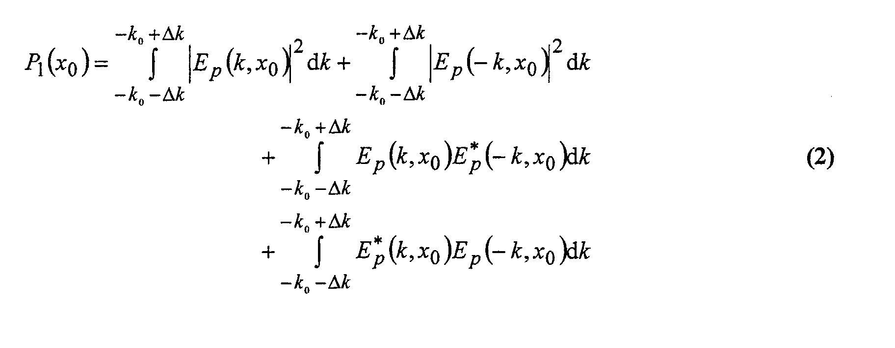
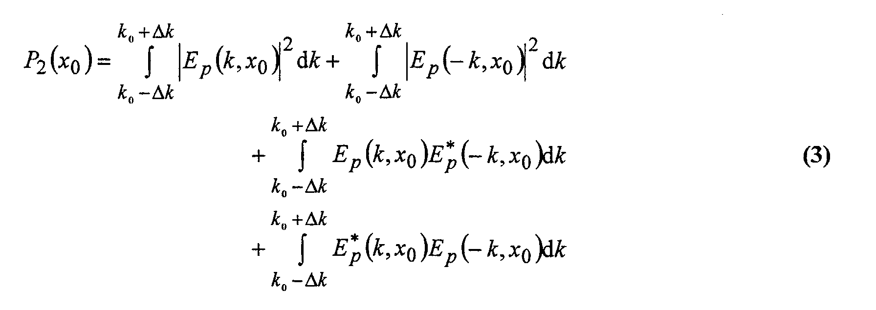
- E p ( k, x 0 ) in the pupil is the Fourier transform (FT) of E nf ( x, x 0 ):
- E p ( k,x 0 ) [ A e ( k ) + j B e ( k )]e j kx 0 + [j A o ( k ) - B o ( k )]e j kx 0
- the real-valued functions A e ( k ), A o ( k ), B e ( k ) and B o ( k ) are the Fourier Transforms of the functions a e ( k ), a o ( k ), b e ( k ) and b 0 ( k ).
- This equation is quite meaningless in this generic formulation.
- E p ( k, x 0 ) A e ( k )e j kx 0
- the amplitude A e ( k ) is an even function of k and independent of the marker position.
- phase in the pupil is no longer a straight line so a phase measurement between two arbitrary points in the pupil plane does not necessarily result in a correct measurement of the position.
- phase difference between two conjugate points in the pupil k and -k is independent of the marker shape and only determined by the marker position. So the intensity in the pupil plane of the alignment system 10 is:
- Figure 13 clarifies how Z is constructed. This Figure also shows how the additional phase term ⁇ ( k ) is introduced by the asymmetric component Z o ( k ). Figure 13 shows that the phase term ⁇ ( k ) has the property ⁇ ( k ) ⁇ (- k ) ⁇ 0 so ⁇ ( k ) contains always an odd component and possibly a small (but irrelevant) even component.
- the even phase variation is irrelevant since only odd phase variations are detected. Moreover, as stated earlier, the position information is contained in the slope of the net phase in the pupil plane so we only need to consider phase terms that vary linearly with k.
- the total phase variation ⁇ d ( k ) as detected by the alignment system 10 is:
- the higher order terms ( c 3 , c 5 etc.) of the measured phase ⁇ d ( k ) are only a function of the unknown asymmetry and here lies a solution to this problem.
- a measurement of the higher order terms may allow a determination of the linear asymmetry term c 1 .
- the field in the pupil consists of bright areas (large amplitude
- the bright areas correspond to the odd diffraction orders of a 50 % duty-cycle grating.
- the even orders of such a grating are the dark areas.
- >>
- ⁇ ( k ) will be very small and barely varies with small changes in asymmetry that may be caused by process variations. In principle these bright areas can be used to measure the higher order terms but the measurement accuracy may be too limited.
- the theory of asymmetry detection will now be further explained with reference to a one-dimensional example.
- the marker is illuminated with an intensity profile shown in Figure 16.
- the optical power of the incident beam is 1 mW and the full width is roughly 100 ⁇ m.
- the wavelength of the illumination beam is 633 nm.
- the example is 1-dimensional so the bar extends to infinity in the y-direction.
- the reflection coefficient of this bar is unity.
- the extension of this marker to a periodic structure i.e. a grating is discussed later.
- the bar has a relatively small phase depth and is also very small compared to the width of the illumination spot (note the different scales in Figures 16 and 17). Consequently, the reflected light will have a very strong specular reflection and only a very small amount of light will be diffracted. This is clearly demonstrated in the intensity distribution in the far field as shown in Figure 18.
- the strong specular peak is clearly visible and reaches a peak intensity of 1.5 ⁇ 10 -4 W/1.3 mrad.
- the full width of the specular reflection is 20 mrad and it can be verified through integration that practically all the incident power is specularly reflected.
- the diffracted light reaches a peak intensity of only 1.5 ⁇ 10 -7 W/1.3 mrad so a detector with an aperture of 5 mrad captures a total optical power of only 0.6 ⁇ W.
- the intensity is zero for sin( ⁇ ) ⁇ 0.32 which would be the location of the second diffraction order if this 2 ⁇ m wide bar were repeated with a 4 ⁇ m period.
- the marker is perfectly symmetric so the phase difference as detected by the alignment system 10 should yield a perfectly straight line with a slope that is proportional to the marker position. This is clearly visible in Figure 19 which shows the measured phase as a function of far-field angle.
- the small spikes are numerical anomalies that are located at the points of zero intensity. In practice these points correspond to phase-singularities that occur in areas with zero intensity. Apart from these numerical artifacts it can be clearly seen that the phase is a straight line with zero slope which indicates that the marker is at the aligned position.
- Figure 21 shows the intensity of the light in the pupil plane. Compared to the symmetric case, the shape has barely changed. However, the intensity in the dark area has increased considerably. This is already an indication that variations in the 'dark' areas in the pupil plane are a good indicator of (changes in) asymmetry.
- phase error 0.058 4 ⁇ ⁇ 4 ⁇ m ⁇ 18 nm
- the contrast curve of Figure 23 indicates that the contrast is sufficiently high to allow accurate phase measurements. However, it must be emphasized that other asymmetry types may exist where the contrast can be significantly degraded.
- the isolated structure discussed above will be periodically repeated to concentrate the scattered light in discrete diffraction orders.
- This periodic repetition does not change the concept of asymmetry measurement since this periodic repetition only influences the even phase distribution ⁇ e ( k ) and the amplitude
- the odd phase variation that is introduced by the asymmetry is unchanged.
- the complex reflection coefficient of the isolated structure is r ( x ) and this structure results in a complex field Z(k) in the pupil.
- Z g (k) is obtained by multiplying Z(k) with a real valued even function f(k). This function can become negative which gives rise to phase jumps in Z g (k). These phase jumps, however, are always symmetrical.
- Figure 25 shows the intensity in the far field for the marker with a 4-nm rooftop that is repeated 5 times.
- the 1 st and 3 rd diffraction orders are clearly visible in the graph.
- the intensity ration between these orders is slightly higher than the expected (1/3) 2 ratio which is caused by Huygen's obliquity factor [1+ cos( ⁇ )]/2 in the diffracted field.
- the intensity of the weak odd order has also increased considerably. Between the orders the intensity exhibits rapid oscillations.
- the peak intensities correspond to quite an appreciable amount of photons.
- a very fundamental limitation of the accuracy of an asymmetry measurement technique is surface roughness of the marker. This is not surprising since surface roughness can be considered a form of random asymmetry that introduces large and noisy phase variations in the dark regions of the interference pattern. This is demonstrated in the example below for the same grating as used in the previous section. This time, however, a 0.5 nm surface roughness was added with an average grain size of 1 ⁇ m. The illumination spot had a width of 200 ⁇ m.
- Figure 28 shows measured phase in the far field and the impact of surface roughness is very clearly visible. At first sight it appears to be quite dramatic. Fortunately, there are a few reasons why the noise will be less dramatic in practical cases. First of all, the large spikes correspond to points of zero intensity (the singularities). Since the detector always has a finite spatial extent these effects will be suppressed in the detection. Secondly, in this particular example the illumination spot size is large compared to the grating width so the sensor 'sees' a lot of roughness effects in regions that are not interesting. This argument again stresses the importance of an optimum illumination spot.
- the linear term of the measured phase ⁇ d contains the position information. However, this position is affected by the presence of asymmetry. In order to know this asymmetry contribution we must know the 'shape' of the asymmetry as accurately as possible. The non-linear variation of the measured phase ⁇ d gives information about the asymmetry. Each asymmetry has its own unique fingerprint.
- a predictive recipe-like approach offers more possibilities with the present invention since more data can be available which allows the use of statistical techniques.
- a particularly useful approach is the use of 'inverse problem' techniques that are also used in scatterometry.
- An alignment sensor should preferably generate a localized signal that peaks very sharply at the location of the marker.
- the realization of such a sensor would introduce a lot of practical problems like signal-to-noise ratio since a narrow peak requires a large measurement bandwidth.
- phase grating alignment sensors are often used since these sensors generate a narrow-bandwidth time-limited harmonic signal.
- phase grating alignment sensors require a 'capturing' mechanism that decides which of the peaks corresponds to the marker position.
- two capturing mechanisms are possible. The first makes use of the camera image that is available from the 0 th order, as discussed above. The second uses the signals that are detected in the pupil plane and requires a split photo diode. Both methods require only one short grating.
- the objective lens 12 has a large NA, e.g. of 0.6, and the absence of spatial filtering yields a 'sharp' image with a resolution of the order of 1-2 ⁇ m which is more than enough to allow various camera-based capturing algorithms, using advanced image processing techniques.
- a camera image after the polarizing beam splitter includes two overlapping and shifted images of the marker whereas a camera image created with a separate polarizer can show two individual images of the marker.
- the first type of image yields two images that are 180° degrees rotated relative to each other which is an advantage for capturing algorithms since the shape of the contour of the partially overlapping marker images can give accurate information about the marker location.
- the pre-alignment error exceeds the scribe lane width, the marker in one image will be projected in the product structure of the other image and this may lead to robustness problems since the product structure acts as a noise source that degrades the robustness of the image processing algorithms.
- the present invention can also make use of the known technique whereby two gratings with slightly different periods generate two harmonic alignment signals with a slightly different frequency.
- the location where two peaks of the two signals coincide is defined as the marker position.
- the present invention provides another capturing alternative that is especially suited to short markers with broad diffraction orders.
- This technique is based on the fact that the entire pupil plane is available. However, it only works if the illumination spot is larger than the marker length.
- the main advantage of this technique is the need for only one grating instead of two separate gratings. The technique will now be explained further.
- the first diffraction order has a spatial frequency k 1 of:
- the diffraction order has a sin( k )/ k shape and the full width of the main lobe is:
- the alignment signal of the 1 st diffraction order of this grating is measured with a split detector. Each detector element captures one half of the main lobe. The center line between the two elements is centered on the peak of the diffraction order. The average spatial frequency captured by these two detectors is about: Both detectors measure a signal with a slight difference in spatial frequency. The effective wavelength of these two signals is: So the capturing range is equal to ⁇ W
- a second embodiment of the invention utilizes a fiber array for conducting light form the pupil plane to a detector array but is otherwise the same as the first embodiment and can be used in the same ways.
- Figure 29 shows the detector part of the alignment system of the second embodiment.
- the light from the self-referencing interferometer (not shown in Figure 29) is split by polarizing beam splitter 19 into two branches, one of which is directed to a camera for capturing purposes (coarse alignment) and the other is used for the fine alignment measurement.
- the fine alignment branch comprises an optical system of lenses 31, 33 which re-image the pupil plane of the self-referencing interferometer onto an array of optical fibers 35 which conduct it to a remote detector array, e.g. an array of photodiodes or a CCD.
- the lens 31 also creates an intermediate image of the marker at the position of which an image plane filter 32, acting as an aperture stop, is provided.
- the fiber bundle 35 can be arranged, with a suitable array of detectors at the end of the bundle, so that the intensity in a plurality of different positions in the pupil plane, in which the two images overlap and interfere, can be determined.
- the resulting data can be processed to derive the required position information.
- the signals from pairs of fibers on opposite sides of the optical axis of the detection branch are added. This can be done by combining the pairs of fibers, by having both fibers of a pair end on the same photodetector or electronically.
- the detector array may comprise a plurality of discrete detectors connected to individual fibers or pairs of fibers or a position sensitive detector, such as a CCD array.
- the detector array itself rather than the input end of the fiber bundle, may be located in the pupil plane but the fiber bundle allows the detector array and its associated electronics, e.g. pre-amplifiers, to be located away from temperature sensitive parts of the apparatus.
- a further spatial filter 34 removes the 0 th order.
- Figure 30 The use of the camera for capturing is shown in Figure 30.
- This figure shows the two images of the marker, top two rows, and the sum image seen by the camera, bottom row, for various positions of the marker.
- the marker In column A, the marker is coarsely aligned and the image seen by the camera has dark and light lines with a high contrast between them.
- the images move in opposite directions leading first to an evenly gray image, shown in column B, then to a pattern of lines, shown in column C, but with an extra line and with less contrast for the outer lines. Further movement leads again to a gray image, column D, and an image with lines, column E, again with an additional line.
- Image recognition software can readily detect the image with a minimum number of lines and maximum contrast.
- a third embodiment of the invention is the same as the first embodiment, save in the construction of the detection branch, which is shown in Figure 31.
- the detection branch of the third embodiment includes a polarizer (not shown in Figure 31), optical system 31, 33 and image plane filter 32 as in the second embodiment.
- the third embodiment has a spatial light modulator, e.g. an LCD array (light valve) or micro-mirror array, 39 that is programmed to select part of the pupil plane, the light from which is collected by lens 40 onto fiber 41, which leads to a photodetector 42.
- a spatial light modulator e.g. an LCD array (light valve) or micro-mirror array
- the spatial light modulator 39 is programmed to select the two beams of a particular order from the overlapped Fourier transforms of the marker images, the intensity of which can then be measured by detector 42 as the marker is scanned to derive the desired positional information. Where the marker is illuminated with a multi-wavelength light source, the different wavelengths can be separated and separately detected in the detector 42.
- the third embodiment has a number of advantages, principal among which is that the alignment system can be used with any marker having 180° rotational symmetry, without having to modify the hardware. All that is required is that the spatial light modulator is appropriately programmed, which can be performed on the fly, even to align to different markers on the same substrate.
- the alignment system of the third embodiment can thus be compatible with known markers such as gratings, checkerboards, boxes, frames, chevrons, etc..
- the complete pupil plane can be sampled and analyzed by repeated scans of the marker with different settings of the spatial light modulator 39.
- a polarizing beam splitter is used to create the necessary interference between the overlapping images, then, as mentioned above, two beams containing the positional information are created and the components shown in Figure 31 may be duplicated in a separate branch to allow simultaneous detection of two orders.
- a spatial light modulator capable of selectively redirecting light into a plurality of different directions, such as a micro-mirror array with more than two mirror positions, may be used with a corresponding number of collecting lenses, fibers and detectors, to allow detection of multiple orders in a single branch.
- fiber 41 it is possible to dispense with fiber 41 and position a detector at the focus of collector lens 40 but the use of fiber 41 allows a heat generating or bulky detector to be located away from heat sensitive components or where more space is available.
- Figures 32 and 33 An order-combining prism which may be used in embodiments of the present invention is shown in Figures 32 and 33, of which Figure 32 shows the prism in exploded form and Figure 33 in assembled form.
- the order-combining prism 50 In its assembled form the basic shape of the order-combining prism 50 is a triangular prism with a bottom, entrance face 55 and a side, exit face 56.
- the prism is divided into two halves 51, 54 by a diagonal join 57.
- a positive order +n enters the bottom face of the first half 51, makes a total internal reflection from a side face 58 towards the join 57.
- the positive order is reflected backwards from the join 57, which acts as a beamsplitter surface to a quarter waveplate and mirror which are mounted to the rear face of the prism 50. These serve to rotate the polarization of the positive order and return it through the joint, beamsplitter surface 57 to exit out of the front face 56 of the prism.
- a negative order enters the bottom of the second half 54 and is totally internally reflected from a second side face 59 and the joint, beamsplitter surface 57 to also exit through the front face 56.
- Figure 33 shows that if the prism is located to receive symmetrically about its center positive and negative orders, orders +1 to +4 and -1 to -4 are shown, the corresponding + and - orders are combined but the first, second, etc. orders are maintained separate.
- the order-combining prism may be used in the pupil plane of embodiments of the present invention to combine the opposite orders, which carry essentially the same information, for detection.
- Use of the order-combining prism doubles the intensity of the signal to be detected, enabling use of a lower-power light source.
- the resulting symmetric arrangement averages out asymmetry-induced differences between positive and negative diffraction orders.
- the order-combining prism of the invention is very compact and is particularly useful in situations where the space available is limited.
- the order-combining prism may have other uses than in the pupil plane of an alignment system based around a self-referencing interferometer and in particular may be used in any arrangement where it is desired to combine diffractive orders located in a single plane.
- the prism may also be modified, e.g. to provide an equal optical path length in its two sides.
- the alignment system described above may be used for alignment to markers provided on a mask or a table as well as on a substrate.
Landscapes
- Physics & Mathematics (AREA)
- General Physics & Mathematics (AREA)
- Engineering & Computer Science (AREA)
- Multimedia (AREA)
- Exposure And Positioning Against Photoresist Photosensitive Materials (AREA)
- Exposure Of Semiconductors, Excluding Electron Or Ion Beam Exposure (AREA)
- Length Measuring Devices By Optical Means (AREA)
Abstract
Description
- a radiation system for supplying a projection beam of radiation;
- a support structure for supporting patterning means, the patterning means serving to pattern the projection beam according to a desired pattern;
- a substrate table for holding a substrate;
- a projection system for projecting the patterned beam onto a target portion of the substrate; and
- an alignment system having a self-referencing interferometer for projecting two overlapping images of an alignment mark that are relatively rotated by 180°.
- A mask. The concept of a mask is well known in lithography, and it includes mask types such as binary, alternating phase-shift, and attenuated phase-shift, as well as various hybrid mask types. Placement of such a mask in the radiation beam causes selective transmission (in the case of a transmissive mask) or reflection (in the case of a reflective mask) of the radiation impinging on the mask, according to the pattern on the mask. In the case of a mask, the support structure will generally be a mask table, which ensures that the mask can be held at a desired position in the incoming radiation beam, and that it can be moved relative to the beam if so desired.
- A programmable mirror array. One example of such a device is a matrix-addressable surface having a viscoelastic control layer and a reflective surface. The basic principle behind such an apparatus is that (for example) addressed areas of the reflective surface reflect incident light as diffracted light, whereas unaddressed areas reflect incident light as undiffracted light. Using an appropriate filter, the said undiffracted light can be filtered out of the reflected beam, leaving only the diffracted light behind; in this manner, the beam becomes patterned according to the addressing pattern of the matrix-addressable surface. An alternative embodiment of a programmable mirror array employs a matrix arrangement of tiny mirrors, each of which can be individually tilted about an axis by applying a suitable localized electric field, or by employing piezoelectric actuation means. Once again, the mirrors are matrix-addressable, such that addressed mirrors will reflect an incoming radiation beam in a different direction to unaddressed mirrors; in this manner, the reflected beam is patterned according to the addressing pattern of the matrix-addressable mirrors. The required matrix addressing can be performed using suitable electronic means. In both of the situations described hereabove, the patterning means can comprise one or more programmable mirror arrays. More information on mirror arrays as here referred to can be gleaned, for example, from United States Patents US 5,296,891 and US 5,523,193, and PCT patent applications WO 98/38597 and WO 98/33096, which are incorporated herein by reference. In the case of a programmable mirror array, the said support structure may be embodied as a frame or table, for example, which may be fixed or movable as required.
- A programmable LCD array. An example of such a construction is given in United States Patent US 5,229,872, which is incorporated herein by reference. As above, the support structure in this case may be embodied as a frame or table, for example, which may be fixed or movable as required.
- providing a substrate that is at least partially covered by a layer of radiation-sensitive material;
- providing a projection beam of radiation using a radiation system;
- using patterning means to endow the projection beam with a pattern in its cross-section;
- projecting the patterned beam of radiation onto a target portion of the layer of radiation-sensitive material, and
- before or after said step of projecting, performing an alignment to an alignment mark on said substrate using a self-referencing interferometer that projects two overlapping images of said alignment mark that are relatively rotated by 180°;
- a radiation system Ex, IL, for supplying a projection beam PB of radiation (e.g. DUV radiation), which in this particular case also comprises a radiation source LA;
- a first object table (mask table) MT provided with a mask holder for holding a mask MA (e.g. a reticle), and connected to first positioning means for accurately positioning the mask with respect to item PL;
- a second object table (substrate table) WT provided with a substrate holder for holding a substrate W (e.g. a resist-coated silicon wafer), and connected to second positioning means for accurately positioning the substrate with respect to item PL;
- a projection system ("lens") PL (e.g. a refractive lens system) for imaging an irradiated portion of the mask MA onto a target portion C (e.g. comprising one or more dies) of the substrate W.

| Δλ [nm], @ w=20 µm | |||
| λ [nm] | Pb =1.5 µm | Pb =1.2 µm | Pb =1.0 µm |
| 532 | 37 | 29 | 23 |
| 633 | 43 | 32 | 25 |
| 780 | 50 | 36 | 24 |
| 850 | 53 | 36 | 22 |



















Claims (21)
- A lithographic projection apparatus comprising:characterized in that said alignment system further comprises a detector system for detecting light intensities at a plurality of different positions in a pupil plane of said self-referencing interferometer.a radiation system for providing a projection beam of radiation;a support structure for supporting patterning means, the patterning means serving to pattern the projection beam according to a desired pattern;a substrate table for holding a substrate;a projection system for projecting the patterned beam onto a target portion of the substrate, andan alignment system having a self-referencing interferometer for projecting two overlapping images of an alignment mark that are relatively rotated by 180°;
- Apparatus according to claim 1 wherein at least two positions of said plurality of positions are located substantially at the positions of different diffraction orders produced by said alignment marker.
- Apparatus according to claim 1 or 2 wherein at least two positions of said plurality of positions are located substantially equidistantly from and on opposite sides of a diffraction order produced by said alignment marker.
- Apparatus according to claim 1, 2 or 3 wherein said detector system comprises a plurality of detecting elements located substantially in said pupil plane.
- Apparatus according to claim 1, 2 or 3 wherein said detector system comprises a plurality of optical fibers each having an input end located substantially in said pupil plane and an output end for directing light conducted through the fiber onto one of a plurality of detecting elements.
- Apparatus according to claim 5 wherein each of said fibers is arranged to direct light onto a respective one of said detector elements.
- Apparatus according to claim 5 wherein said fibers are provided in pairs, the input ends of the fibers of a pair being symmetrically located in said pupil plane, and the light conducted by the fibers of a pair is directed onto the same detection element.
- Apparatus according to any one of claims 4 to 7 wherein said detection elements comprise photodiodes.
- Apparatus according to any one of claims 4 to 7 wherein said detection elements are elements of a CCD array.
- Apparatus according to claim 1, 2 or 3 wherein said detection system comprises a spatial light modulator provided in said pupil plane, said spatial light modulator being controllable to pass light from selected portions of said pupil plane, and a collector for collecting light passed by said spatial light modulator onto a detection element.
- Apparatus according to any one of the preceding claims wherein said alignment system comprises means for illuminating an alignment marker with light of a plurality of different wavelengths and said detection system comprises wavelength de-multiplexing means for directing light of different wavelengths to different detecting elements.
- Apparatus according to claim 11 wherein said wavelength de-multiplexing means comprises a blazed grating.
- Apparatus according to any one of the preceding claims wherein said alignment system comprises an aperture stop in an image plane located between said self-referencing interferometer and said pupil plane.
- Apparatus according to claim 13 wherein said aperture stop has a controllable aperture.
- Apparatus according to any one of the preceding claims wherein said alignment system includes a polarizing beam splitter for directing light output by said self-referencing interferometer into two beams and wherein there are two detector systems receiving light from respective ones of said beams.
- Apparatus according to any one of the preceding claims wherein said alignment system includes a polarizing beam splitter for directing light output by said self-referencing interferometer into two beams, one of said beams being received by said by said detector system and the other by a camera.
- Apparatus according to any one of the preceding claims wherein said detector system comprises an order-combining prism for receiving a set of positive orders and a corresponding set of negative orders through an input face and outputting a combined set of orders through an output face perpendicular to said input face, said prism comprising:first and second halves joined at a beam splitting surface perpendicular to said input face and at 45° to said output face; anda quarter waveplate and a mirror provided adjacent a further face of said first half of said prism opposite said output face.
- A device manufacturing method comprising the steps of:characterized that said step of aligning comprises measuring the intensities of light at a plurality of different positions in a pupil plane where Fourier transforms of said images of said alignment mark interfere.providing a substrate that is at least partially covered by a layer of radiation-sensitive material;providing a projection beam of radiation using a radiation system;using patterning means to endow the projection beam with a pattern in its cross-section;projecting the patterned beam of radiation onto a target portion of the layer of radiation-sensitive material, andbefore or after said step of projecting, performing an alignment to an alignment mark on said substrate using a self-referencing interferometer that projects two overlapping images that are relatively rotated by 180° of said alignment mark;
- A method according to claim 18 wherein said plurality of different positions include positions corresponding to different diffraction orders in said Fourier transforms and fine positional information is determined from the relative phases of variations of the intensities of said different orders.
- A method according to claim 18 or 19 wherein said plurality of different positions comprise two positions equidistantly spaced on opposite sides of a diffraction order in said pupil plane and wherein coarse positional information is determined from the relative phases of intensity variations at said two positions on opposite sides of a diffraction order.
- A method according to claim 18, 19 or 20 further comprising the step of measuring phase variations in dark areas of said pupil plane to detect asymmetries in said alignment marker.
Priority Applications (2)
| Application Number | Priority Date | Filing Date | Title |
|---|---|---|---|
| EP20030253494 EP1372040B1 (en) | 2002-06-11 | 2003-06-04 | Lithographic apparatus and device manufacturing method |
| EP06026407A EP1764655A3 (en) | 2002-06-11 | 2003-06-04 | Lithographic apparatus and device manufacturing method |
Applications Claiming Priority (3)
| Application Number | Priority Date | Filing Date | Title |
|---|---|---|---|
| EP02254057 | 2002-06-11 | ||
| EP02254057 | 2002-06-11 | ||
| EP20030253494 EP1372040B1 (en) | 2002-06-11 | 2003-06-04 | Lithographic apparatus and device manufacturing method |
Related Child Applications (1)
| Application Number | Title | Priority Date | Filing Date |
|---|---|---|---|
| EP06026407A Division EP1764655A3 (en) | 2002-06-11 | 2003-06-04 | Lithographic apparatus and device manufacturing method |
Publications (3)
| Publication Number | Publication Date |
|---|---|
| EP1372040A2 true EP1372040A2 (en) | 2003-12-17 |
| EP1372040A3 EP1372040A3 (en) | 2006-04-19 |
| EP1372040B1 EP1372040B1 (en) | 2008-03-05 |
Family
ID=29585713
Family Applications (2)
| Application Number | Title | Priority Date | Filing Date |
|---|---|---|---|
| EP06026407A Withdrawn EP1764655A3 (en) | 2002-06-11 | 2003-06-04 | Lithographic apparatus and device manufacturing method |
| EP20030253494 Expired - Lifetime EP1372040B1 (en) | 2002-06-11 | 2003-06-04 | Lithographic apparatus and device manufacturing method |
Family Applications Before (1)
| Application Number | Title | Priority Date | Filing Date |
|---|---|---|---|
| EP06026407A Withdrawn EP1764655A3 (en) | 2002-06-11 | 2003-06-04 | Lithographic apparatus and device manufacturing method |
Country Status (1)
| Country | Link |
|---|---|
| EP (2) | EP1764655A3 (en) |
Cited By (30)
| Publication number | Priority date | Publication date | Assignee | Title |
|---|---|---|---|---|
| US7570358B2 (en) | 2007-03-30 | 2009-08-04 | Asml Netherlands Bv | Angularly resolved scatterometer, inspection method, lithographic apparatus, lithographic processing cell device manufacturing method and alignment sensor |
| EP2093617A2 (en) | 2008-02-21 | 2009-08-26 | ASML Netherlands B.V. | Mark structure for coarse wafer alignment and method for manufacturing such a mark structure |
| EP2103995A2 (en) | 2008-03-21 | 2009-09-23 | ASML Netherlands B.V. | Method for coarse wafer alignment in a lithographic apparatus |
| EP2131245A2 (en) | 2008-06-02 | 2009-12-09 | ASML Netherlands BV | Lithographic apparatus and its focus determination method |
| US7798676B2 (en) | 2004-12-23 | 2010-09-21 | Carl Zeiss Smt Ag | Filter device for the compensation of an asymmetric pupil illumination |
| US20100245792A1 (en) * | 2009-03-26 | 2010-09-30 | Asml Netherlands B.V. | Alignment Measurement Arrangement, Alignment Measurement Method, Device Manufacturing Method and Lithographic Apparatus |
| US7968120B2 (en) * | 2001-09-28 | 2011-06-28 | Mcneil-Ppc, Inc. | Modified release dosage forms |
| CN101561640B (en) * | 2008-02-07 | 2011-08-10 | Asml荷兰有限公司 | Method for determining exposure settings and lithographic exposure apparatus |
| RU2438153C1 (en) * | 2010-07-15 | 2011-12-27 | Государственное образовательное учреждение высшего профессионального образования "Сибирская государственная геодезическая академия" (ГОУ ВПО "СГГА") | Apparatus for exposure when forming nanosize structures and method of forming nanosize structures |
| US8115938B2 (en) | 2008-03-04 | 2012-02-14 | Asml Netherlands B.V. | Method of providing alignment marks, device manufacturing method and lithographic apparatus |
| US8208121B2 (en) | 2008-02-01 | 2012-06-26 | Asml Netherlands B.V. | Alignment mark and a method of aligning a substrate comprising such an alignment mark |
| CN102778301A (en) * | 2012-07-31 | 2012-11-14 | 中国科学院上海光学精密机械研究所 | Real-time measuring device of self-reference spectrum interference femtosecond laser pulse |
| US8610898B2 (en) | 2010-09-08 | 2013-12-17 | Asml Netherlands B.V. | Self-referencing interferometer, alignment system, and lithographic apparatus |
| WO2016192865A1 (en) * | 2015-06-05 | 2016-12-08 | Asml Netherlands B.V. | Alignment system |
| WO2017045874A1 (en) * | 2015-09-18 | 2017-03-23 | Asml Netherlands B.V. | Alignment sensor for lithographic apparatus |
| US10036962B2 (en) | 2013-12-13 | 2018-07-31 | Asml Netherlands B.V. | Inspection apparatus and methods, lithographic system and device manufacturing method |
| WO2020043582A1 (en) | 2018-08-29 | 2020-03-05 | Asml Holding N.V. | Compact alignment sensor arrangements |
| CN112305741A (en) * | 2020-05-27 | 2021-02-02 | 南方科技大学 | Multi-focus optical system |
| WO2021063663A1 (en) | 2019-09-30 | 2021-04-08 | Asml Holding N.V. | Alignment sensor with modulated light source |
| WO2021078474A1 (en) | 2019-10-21 | 2021-04-29 | Asml Holding N.V. | Apparatus for and method of sensing alignment marks |
| CN113134971A (en) * | 2021-04-26 | 2021-07-20 | 长春理工大学 | System and method for manufacturing bionic sharkskin structure |
| WO2021156069A1 (en) | 2020-02-05 | 2021-08-12 | Asml Holding N.V. | Apparatus for sensing alignment marks |
| WO2021259645A1 (en) | 2020-06-24 | 2021-12-30 | Asml Holding N.V. | Self-referencing integrated alignment sensor |
| CN114207530A (en) * | 2019-08-09 | 2022-03-18 | Asml荷兰有限公司 | Phase modulator for reducing mark size in alignment |
| WO2022207395A1 (en) | 2021-03-29 | 2022-10-06 | Asml Netherlands B.V. | Asymmetry extended grid model for wafer alignment |
| WO2022258371A1 (en) | 2021-06-08 | 2022-12-15 | Asml Netherlands B.V. | Intensity imbalance calibration on an overfilled bidirectional mark |
| WO2023016773A1 (en) | 2021-08-12 | 2023-02-16 | Asml Netherlands B.V. | Intensity measurements using off-axis illumination |
| WO2023117263A1 (en) | 2021-12-20 | 2023-06-29 | Asml Netherlands B.V. | Method and apparatus for lithographic imaging |
| EP3790280B1 (en) * | 2019-09-03 | 2023-11-15 | eSMART Technologies SA | System and methods of device pairing |
| EP4300178A1 (en) * | 2022-06-30 | 2024-01-03 | Mycronic Ab | Electrical crosstalk cancellation in acoustooptical modulators |
Families Citing this family (6)
| Publication number | Priority date | Publication date | Assignee | Title |
|---|---|---|---|---|
| US7580131B2 (en) * | 2007-04-17 | 2009-08-25 | Asml Netherlands B.V. | Angularly resolved scatterometer and inspection method |
| CN106547170B (en) * | 2015-09-17 | 2019-09-17 | 上海微电子装备(集团)股份有限公司 | A kind of label alignment device and alignment methods |
| CN112415870B (en) * | 2019-08-23 | 2022-11-25 | 上海微电子装备(集团)股份有限公司 | Prism assembly, optical system, photoetching equipment and light field rotation method |
| WO2021259646A1 (en) | 2020-06-24 | 2021-12-30 | Asml Netherlands B.V. | Monolithic particle inspection device |
| CN117642701A (en) | 2021-07-16 | 2024-03-01 | Asml荷兰有限公司 | Measurement methods and equipment |
| CN119923598A (en) * | 2022-10-11 | 2025-05-02 | Asml荷兰有限公司 | Detection system using metasurfaces and integrated optical systems for lithography |
Family Cites Families (7)
| Publication number | Priority date | Publication date | Assignee | Title |
|---|---|---|---|---|
| DE3404963C2 (en) * | 1984-02-11 | 1986-09-25 | Fraunhofer-Gesellschaft zur Förderung der angewandten Forschung e.V., 8000 München | Laser interferometer for length measurement |
| US4687332A (en) * | 1985-10-15 | 1987-08-18 | Lockheed Missiles & Space Company, Inc. | Self-referencing scan-shear interferometer |
| JP2902421B2 (en) * | 1989-10-16 | 1999-06-07 | 旭光学工業株式会社 | Interferometer |
| DE4028050A1 (en) * | 1990-09-05 | 1992-03-12 | Kerner Anna | Grating interferometer measuring straightness of machine guides - detects offset of directional beam w.r.t. grating and phase shift indicating deviation from linearity |
| JP3653827B2 (en) * | 1995-10-20 | 2005-06-02 | 株式会社ニコン | Interferometer |
| US6628406B1 (en) * | 2000-04-20 | 2003-09-30 | Justin L. Kreuzer | Self referencing mark independent alignment sensor |
| JP2002050560A (en) * | 2000-08-02 | 2002-02-15 | Nikon Corp | Stage device, measurement device and measurement method, exposure device and exposure method |
-
2003
- 2003-06-04 EP EP06026407A patent/EP1764655A3/en not_active Withdrawn
- 2003-06-04 EP EP20030253494 patent/EP1372040B1/en not_active Expired - Lifetime
Cited By (56)
| Publication number | Priority date | Publication date | Assignee | Title |
|---|---|---|---|---|
| US7968120B2 (en) * | 2001-09-28 | 2011-06-28 | Mcneil-Ppc, Inc. | Modified release dosage forms |
| US8025427B2 (en) | 2004-12-23 | 2011-09-27 | Carl Zeiss Smt Gmbh | Filter device for the compensation of an asymmetric pupil illumination |
| US8480261B2 (en) | 2004-12-23 | 2013-07-09 | Carl Zeiss Smt Gmbh | Filter device for the compensation of an asymmetric pupil illumination |
| US8246211B2 (en) | 2004-12-23 | 2012-08-21 | Carl Zeiss Smt Gmbh | Filter device for the compensation of an asymmetric pupil illumination |
| US7798676B2 (en) | 2004-12-23 | 2010-09-21 | Carl Zeiss Smt Ag | Filter device for the compensation of an asymmetric pupil illumination |
| US8636386B2 (en) | 2004-12-23 | 2014-01-28 | Carl Zeiss Smt Gmbh | Filter device for the compensation of an asymmetric pupil illumination |
| US7570358B2 (en) | 2007-03-30 | 2009-08-04 | Asml Netherlands Bv | Angularly resolved scatterometer, inspection method, lithographic apparatus, lithographic processing cell device manufacturing method and alignment sensor |
| US8031337B2 (en) | 2007-03-30 | 2011-10-04 | Asml Netherlands B.V. | Angularly resolved scatterometer |
| US8208121B2 (en) | 2008-02-01 | 2012-06-26 | Asml Netherlands B.V. | Alignment mark and a method of aligning a substrate comprising such an alignment mark |
| US8208118B2 (en) | 2008-02-07 | 2012-06-26 | Asml Netherlands B.V. | Method for determining exposure settings, lithographic exposure apparatus, computer program and data carrier |
| CN101561640B (en) * | 2008-02-07 | 2011-08-10 | Asml荷兰有限公司 | Method for determining exposure settings and lithographic exposure apparatus |
| EP2093617A2 (en) | 2008-02-21 | 2009-08-26 | ASML Netherlands B.V. | Mark structure for coarse wafer alignment and method for manufacturing such a mark structure |
| US7989966B2 (en) | 2008-02-21 | 2011-08-02 | Asml Netherlands B.V. | Mark structure for coarse wafer alignment and method for manufacturing such a mark structure |
| US8080462B2 (en) | 2008-02-21 | 2011-12-20 | Asml Netherlands B.V. | Mark structure for coarse wafer alignment and method for manufacturing such a mark structure |
| US8115938B2 (en) | 2008-03-04 | 2012-02-14 | Asml Netherlands B.V. | Method of providing alignment marks, device manufacturing method and lithographic apparatus |
| EP2103995A2 (en) | 2008-03-21 | 2009-09-23 | ASML Netherlands B.V. | Method for coarse wafer alignment in a lithographic apparatus |
| US8130366B2 (en) | 2008-03-21 | 2012-03-06 | Asml Netherlands B.V. | Method for coarse wafer alignment in a lithographic apparatus |
| US8264671B2 (en) | 2008-06-02 | 2012-09-11 | Asml Netherlands B.V. | Lithographic apparatus and device manufacturing method |
| EP2131243A2 (en) | 2008-06-02 | 2009-12-09 | ASML Netherlands B.V. | Lithographic apparatus and method for calibrating a stage position |
| EP2131244A2 (en) | 2008-06-02 | 2009-12-09 | ASML Netherlands BV | Lithographic apparatus and method for measuring a pattern property |
| CN101676805B (en) * | 2008-06-02 | 2011-11-02 | Asml荷兰有限公司 | Lithographic apparatus and device manufacturing method |
| US8446564B2 (en) | 2008-06-02 | 2013-05-21 | Asml Netherlands B.V. | Lithographic apparatus and device manufacturing method |
| US8477289B2 (en) | 2008-06-02 | 2013-07-02 | Asml Netherlands B.V. | Position measurement using natural frequency vibration of a pattern |
| EP2131245A2 (en) | 2008-06-02 | 2009-12-09 | ASML Netherlands BV | Lithographic apparatus and its focus determination method |
| US20100245792A1 (en) * | 2009-03-26 | 2010-09-30 | Asml Netherlands B.V. | Alignment Measurement Arrangement, Alignment Measurement Method, Device Manufacturing Method and Lithographic Apparatus |
| JP2010232656A (en) * | 2009-03-26 | 2010-10-14 | Asml Netherlands Bv | Alignment measurement arrangement, alignment measurement method, device manufacturing method, and lithographic apparatus |
| RU2438153C1 (en) * | 2010-07-15 | 2011-12-27 | Государственное образовательное учреждение высшего профессионального образования "Сибирская государственная геодезическая академия" (ГОУ ВПО "СГГА") | Apparatus for exposure when forming nanosize structures and method of forming nanosize structures |
| US8610898B2 (en) | 2010-09-08 | 2013-12-17 | Asml Netherlands B.V. | Self-referencing interferometer, alignment system, and lithographic apparatus |
| CN102778301B (en) * | 2012-07-31 | 2014-10-01 | 中国科学院上海光学精密机械研究所 | Real-time measurement device for self-referencing spectral interference of femtosecond laser pulses |
| CN102778301A (en) * | 2012-07-31 | 2012-11-14 | 中国科学院上海光学精密机械研究所 | Real-time measuring device of self-reference spectrum interference femtosecond laser pulse |
| US10036962B2 (en) | 2013-12-13 | 2018-07-31 | Asml Netherlands B.V. | Inspection apparatus and methods, lithographic system and device manufacturing method |
| US10585363B2 (en) | 2015-06-05 | 2020-03-10 | Asml Netherlands B.V. | Alignment system |
| WO2016192865A1 (en) * | 2015-06-05 | 2016-12-08 | Asml Netherlands B.V. | Alignment system |
| JP2018529104A (en) * | 2015-09-18 | 2018-10-04 | エーエスエムエル ネザーランズ ビー.ブイ. | Alignment sensor for lithographic apparatus |
| US10466601B2 (en) | 2015-09-18 | 2019-11-05 | Asml Netherlands B.V. | Alignment sensor for lithographic apparatus |
| WO2017045874A1 (en) * | 2015-09-18 | 2017-03-23 | Asml Netherlands B.V. | Alignment sensor for lithographic apparatus |
| WO2020043582A1 (en) | 2018-08-29 | 2020-03-05 | Asml Holding N.V. | Compact alignment sensor arrangements |
| US11531280B2 (en) | 2018-08-29 | 2022-12-20 | Asml Holding N.V. | Compact alignment sensor arrangements |
| CN114207530A (en) * | 2019-08-09 | 2022-03-18 | Asml荷兰有限公司 | Phase modulator for reducing mark size in alignment |
| EP3790280B1 (en) * | 2019-09-03 | 2023-11-15 | eSMART Technologies SA | System and methods of device pairing |
| WO2021063663A1 (en) | 2019-09-30 | 2021-04-08 | Asml Holding N.V. | Alignment sensor with modulated light source |
| US11899380B2 (en) | 2019-10-21 | 2024-02-13 | Asml Holding N.V. | Apparatus for and method of sensing alignment marks |
| WO2021078474A1 (en) | 2019-10-21 | 2021-04-29 | Asml Holding N.V. | Apparatus for and method of sensing alignment marks |
| WO2021156069A1 (en) | 2020-02-05 | 2021-08-12 | Asml Holding N.V. | Apparatus for sensing alignment marks |
| US11841628B2 (en) | 2020-02-05 | 2023-12-12 | Asml Holding N.V. | Apparatus for and method of sensing alignment marks |
| CN112305741B (en) * | 2020-05-27 | 2022-07-15 | 南方科技大学 | An axial multifocal optical system |
| CN112305741A (en) * | 2020-05-27 | 2021-02-02 | 南方科技大学 | Multi-focus optical system |
| WO2021259645A1 (en) | 2020-06-24 | 2021-12-30 | Asml Holding N.V. | Self-referencing integrated alignment sensor |
| WO2022207395A1 (en) | 2021-03-29 | 2022-10-06 | Asml Netherlands B.V. | Asymmetry extended grid model for wafer alignment |
| US12461457B2 (en) | 2021-03-29 | 2025-11-04 | Asml Netherlands B.V. | Asymmetry extended grid model for wafer alignment |
| CN113134971A (en) * | 2021-04-26 | 2021-07-20 | 长春理工大学 | System and method for manufacturing bionic sharkskin structure |
| WO2022258371A1 (en) | 2021-06-08 | 2022-12-15 | Asml Netherlands B.V. | Intensity imbalance calibration on an overfilled bidirectional mark |
| WO2023016773A1 (en) | 2021-08-12 | 2023-02-16 | Asml Netherlands B.V. | Intensity measurements using off-axis illumination |
| WO2023117263A1 (en) | 2021-12-20 | 2023-06-29 | Asml Netherlands B.V. | Method and apparatus for lithographic imaging |
| EP4300178A1 (en) * | 2022-06-30 | 2024-01-03 | Mycronic Ab | Electrical crosstalk cancellation in acoustooptical modulators |
| WO2024002688A1 (en) * | 2022-06-30 | 2024-01-04 | Mycronic AB | Electrical crosstalk cancellation in acoustooptical modulators |
Also Published As
| Publication number | Publication date |
|---|---|
| EP1764655A2 (en) | 2007-03-21 |
| EP1372040B1 (en) | 2008-03-05 |
| EP1764655A3 (en) | 2007-09-19 |
| EP1372040A3 (en) | 2006-04-19 |
Similar Documents
| Publication | Publication Date | Title |
|---|---|---|
| EP1372040B1 (en) | Lithographic apparatus and device manufacturing method | |
| US6961116B2 (en) | Lithographic apparatus, device manufacturing method, and device manufactured thereby | |
| EP3387481B1 (en) | Objective lens system | |
| US9778025B2 (en) | Method and apparatus for measuring asymmetry of a microstructure, position measuring method, position measuring apparatus, lithographic apparatus and device manufacturing method | |
| JP6342486B2 (en) | Polarization-independent interferometer | |
| US8681312B2 (en) | Inspection apparatus for lithography | |
| US20090153825A1 (en) | Lithographic apparatus and method | |
| JP5787483B2 (en) | Measuring apparatus and exposure apparatus | |
| CN115698861B (en) | Photolithography equipment, multi-wavelength phase modulation scanning measurement system and method | |
| US10317808B2 (en) | Position sensing arrangement and lithographic apparatus including such an arrangement, position sensing method and device manufacturing method | |
| WO2009100867A1 (en) | Method and appartus for angular-resolved spectroscopic lithography characterization | |
| JP2018517933A (en) | Alignment system | |
| US6963391B2 (en) | Lithographic apparatus and device manufacturing method | |
| JP3029133B2 (en) | Measurement method and device | |
| JP2683409B2 (en) | Positioning device |
Legal Events
| Date | Code | Title | Description |
|---|---|---|---|
| PUAI | Public reference made under article 153(3) epc to a published international application that has entered the european phase |
Free format text: ORIGINAL CODE: 0009012 |
|
| AK | Designated contracting states |
Kind code of ref document: A2 Designated state(s): AT BE BG CH CY CZ DE DK EE ES FI FR GB GR HU IE IT LI LU MC NL PT RO SE SI SK TR |
|
| AX | Request for extension of the european patent |
Extension state: AL LT LV MK |
|
| RAP1 | Party data changed (applicant data changed or rights of an application transferred) |
Owner name: ASML NETHERLANDS B.V. |
|
| PUAL | Search report despatched |
Free format text: ORIGINAL CODE: 0009013 |
|
| AK | Designated contracting states |
Kind code of ref document: A3 Designated state(s): AT BE BG CH CY CZ DE DK EE ES FI FR GB GR HU IE IT LI LU MC NL PT RO SE SI SK TR |
|
| AX | Request for extension of the european patent |
Extension state: AL LT LV MK |
|
| 17P | Request for examination filed |
Effective date: 20061012 |
|
| AKX | Designation fees paid |
Designated state(s): DE FR GB IT NL |
|
| GRAP | Despatch of communication of intention to grant a patent |
Free format text: ORIGINAL CODE: EPIDOSNIGR1 |
|
| GRAS | Grant fee paid |
Free format text: ORIGINAL CODE: EPIDOSNIGR3 |
|
| GRAA | (expected) grant |
Free format text: ORIGINAL CODE: 0009210 |
|
| AK | Designated contracting states |
Kind code of ref document: B1 Designated state(s): DE FR GB IT NL |
|
| REG | Reference to a national code |
Ref country code: GB Ref legal event code: FG4D |
|
| REF | Corresponds to: |
Ref document number: 60319462 Country of ref document: DE Date of ref document: 20080417 Kind code of ref document: P |
|
| PGFP | Annual fee paid to national office [announced via postgrant information from national office to epo] |
Ref country code: IT Payment date: 20080621 Year of fee payment: 6 |
|
| PGFP | Annual fee paid to national office [announced via postgrant information from national office to epo] |
Ref country code: DE Payment date: 20080620 Year of fee payment: 6 |
|
| ET | Fr: translation filed | ||
| PGFP | Annual fee paid to national office [announced via postgrant information from national office to epo] |
Ref country code: GB Payment date: 20080620 Year of fee payment: 6 |
|
| PLBE | No opposition filed within time limit |
Free format text: ORIGINAL CODE: 0009261 |
|
| STAA | Information on the status of an ep patent application or granted ep patent |
Free format text: STATUS: NO OPPOSITION FILED WITHIN TIME LIMIT |
|
| 26N | No opposition filed |
Effective date: 20081208 |
|
| PGFP | Annual fee paid to national office [announced via postgrant information from national office to epo] |
Ref country code: NL Payment date: 20090616 Year of fee payment: 7 |
|
| PGFP | Annual fee paid to national office [announced via postgrant information from national office to epo] |
Ref country code: FR Payment date: 20090615 Year of fee payment: 7 |
|
| GBPC | Gb: european patent ceased through non-payment of renewal fee |
Effective date: 20090604 |
|
| PG25 | Lapsed in a contracting state [announced via postgrant information from national office to epo] |
Ref country code: GB Free format text: LAPSE BECAUSE OF NON-PAYMENT OF DUE FEES Effective date: 20090604 |
|
| PG25 | Lapsed in a contracting state [announced via postgrant information from national office to epo] |
Ref country code: DE Free format text: LAPSE BECAUSE OF NON-PAYMENT OF DUE FEES Effective date: 20100101 |
|
| REG | Reference to a national code |
Ref country code: NL Ref legal event code: V1 Effective date: 20110101 |
|
| REG | Reference to a national code |
Ref country code: FR Ref legal event code: ST Effective date: 20110228 |
|
| PG25 | Lapsed in a contracting state [announced via postgrant information from national office to epo] |
Ref country code: IT Free format text: LAPSE BECAUSE OF NON-PAYMENT OF DUE FEES Effective date: 20090604 |
|
| PG25 | Lapsed in a contracting state [announced via postgrant information from national office to epo] |
Ref country code: NL Free format text: LAPSE BECAUSE OF NON-PAYMENT OF DUE FEES Effective date: 20110101 Ref country code: FR Free format text: LAPSE BECAUSE OF NON-PAYMENT OF DUE FEES Effective date: 20100630 |