EP1372024A1 - Liquid crystal optical phase modulator - Google Patents
Liquid crystal optical phase modulator Download PDFInfo
- Publication number
- EP1372024A1 EP1372024A1 EP02360172A EP02360172A EP1372024A1 EP 1372024 A1 EP1372024 A1 EP 1372024A1 EP 02360172 A EP02360172 A EP 02360172A EP 02360172 A EP02360172 A EP 02360172A EP 1372024 A1 EP1372024 A1 EP 1372024A1
- Authority
- EP
- European Patent Office
- Prior art keywords
- optical
- liquid crystal
- optical device
- segment
- optical waveguide
- Prior art date
- Legal status (The legal status is an assumption and is not a legal conclusion. Google has not performed a legal analysis and makes no representation as to the accuracy of the status listed.)
- Withdrawn
Links
- 230000003287 optical effect Effects 0.000 title claims abstract description 93
- 239000004973 liquid crystal related substance Substances 0.000 title claims abstract description 44
- 238000005253 cladding Methods 0.000 claims abstract description 18
- 239000000463 material Substances 0.000 claims abstract description 15
- 239000000758 substrate Substances 0.000 claims abstract description 8
- 230000005684 electric field Effects 0.000 claims abstract description 6
- 230000010287 polarization Effects 0.000 claims description 17
- 239000005262 ferroelectric liquid crystals (FLCs) Substances 0.000 claims 1
- 239000000835 fiber Substances 0.000 description 7
- VYPSYNLAJGMNEJ-UHFFFAOYSA-N Silicium dioxide Chemical compound O=[Si]=O VYPSYNLAJGMNEJ-UHFFFAOYSA-N 0.000 description 6
- 238000005530 etching Methods 0.000 description 6
- 230000010354 integration Effects 0.000 description 6
- 230000008859 change Effects 0.000 description 5
- 230000000694 effects Effects 0.000 description 4
- 238000004519 manufacturing process Methods 0.000 description 4
- 229910052681 coesite Inorganic materials 0.000 description 3
- 229910052906 cristobalite Inorganic materials 0.000 description 3
- 230000001419 dependent effect Effects 0.000 description 3
- 239000006185 dispersion Substances 0.000 description 3
- 239000011521 glass Substances 0.000 description 3
- 238000000034 method Methods 0.000 description 3
- 230000008569 process Effects 0.000 description 3
- 239000000377 silicon dioxide Substances 0.000 description 3
- 229910052682 stishovite Inorganic materials 0.000 description 3
- 229910052905 tridymite Inorganic materials 0.000 description 3
- 239000004988 Nematic liquid crystal Substances 0.000 description 2
- 230000005540 biological transmission Effects 0.000 description 2
- 239000010408 film Substances 0.000 description 2
- 238000003780 insertion Methods 0.000 description 2
- 230000037431 insertion Effects 0.000 description 2
- 238000012986 modification Methods 0.000 description 2
- 230000004048 modification Effects 0.000 description 2
- 230000008901 benefit Effects 0.000 description 1
- 238000004891 communication Methods 0.000 description 1
- 238000005520 cutting process Methods 0.000 description 1
- 238000000151 deposition Methods 0.000 description 1
- 238000013461 design Methods 0.000 description 1
- 238000011161 development Methods 0.000 description 1
- 238000010438 heat treatment Methods 0.000 description 1
- 238000000206 photolithography Methods 0.000 description 1
- 230000000644 propagated effect Effects 0.000 description 1
- 230000005855 radiation Effects 0.000 description 1
- 230000002441 reversible effect Effects 0.000 description 1
- 230000000630 rising effect Effects 0.000 description 1
- 239000010409 thin film Substances 0.000 description 1
- 230000007704 transition Effects 0.000 description 1
Images


Classifications
-
- G—PHYSICS
- G02—OPTICS
- G02F—OPTICAL DEVICES OR ARRANGEMENTS FOR THE CONTROL OF LIGHT BY MODIFICATION OF THE OPTICAL PROPERTIES OF THE MEDIA OF THE ELEMENTS INVOLVED THEREIN; NON-LINEAR OPTICS; FREQUENCY-CHANGING OF LIGHT; OPTICAL LOGIC ELEMENTS; OPTICAL ANALOGUE/DIGITAL CONVERTERS
- G02F1/00—Devices or arrangements for the control of the intensity, colour, phase, polarisation or direction of light arriving from an independent light source, e.g. switching, gating or modulating; Non-linear optics
- G02F1/01—Devices or arrangements for the control of the intensity, colour, phase, polarisation or direction of light arriving from an independent light source, e.g. switching, gating or modulating; Non-linear optics for the control of the intensity, phase, polarisation or colour
- G02F1/13—Devices or arrangements for the control of the intensity, colour, phase, polarisation or direction of light arriving from an independent light source, e.g. switching, gating or modulating; Non-linear optics for the control of the intensity, phase, polarisation or colour based on liquid crystals, e.g. single liquid crystal display cells
- G02F1/1326—Liquid crystal optical waveguides or liquid crystal cells specially adapted for gating or modulating between optical waveguides
-
- G—PHYSICS
- G02—OPTICS
- G02F—OPTICAL DEVICES OR ARRANGEMENTS FOR THE CONTROL OF LIGHT BY MODIFICATION OF THE OPTICAL PROPERTIES OF THE MEDIA OF THE ELEMENTS INVOLVED THEREIN; NON-LINEAR OPTICS; FREQUENCY-CHANGING OF LIGHT; OPTICAL LOGIC ELEMENTS; OPTICAL ANALOGUE/DIGITAL CONVERTERS
- G02F1/00—Devices or arrangements for the control of the intensity, colour, phase, polarisation or direction of light arriving from an independent light source, e.g. switching, gating or modulating; Non-linear optics
- G02F1/01—Devices or arrangements for the control of the intensity, colour, phase, polarisation or direction of light arriving from an independent light source, e.g. switching, gating or modulating; Non-linear optics for the control of the intensity, phase, polarisation or colour
- G02F1/13—Devices or arrangements for the control of the intensity, colour, phase, polarisation or direction of light arriving from an independent light source, e.g. switching, gating or modulating; Non-linear optics for the control of the intensity, phase, polarisation or colour based on liquid crystals, e.g. single liquid crystal display cells
- G02F1/137—Devices or arrangements for the control of the intensity, colour, phase, polarisation or direction of light arriving from an independent light source, e.g. switching, gating or modulating; Non-linear optics for the control of the intensity, phase, polarisation or colour based on liquid crystals, e.g. single liquid crystal display cells characterised by the electro-optical or magneto-optical effect, e.g. field-induced phase transition, orientation effect, guest-host interaction or dynamic scattering
- G02F1/139—Devices or arrangements for the control of the intensity, colour, phase, polarisation or direction of light arriving from an independent light source, e.g. switching, gating or modulating; Non-linear optics for the control of the intensity, phase, polarisation or colour based on liquid crystals, e.g. single liquid crystal display cells characterised by the electro-optical or magneto-optical effect, e.g. field-induced phase transition, orientation effect, guest-host interaction or dynamic scattering based on orientation effects in which the liquid crystal remains transparent
- G02F1/141—Devices or arrangements for the control of the intensity, colour, phase, polarisation or direction of light arriving from an independent light source, e.g. switching, gating or modulating; Non-linear optics for the control of the intensity, phase, polarisation or colour based on liquid crystals, e.g. single liquid crystal display cells characterised by the electro-optical or magneto-optical effect, e.g. field-induced phase transition, orientation effect, guest-host interaction or dynamic scattering based on orientation effects in which the liquid crystal remains transparent using ferroelectric liquid crystals
-
- G—PHYSICS
- G02—OPTICS
- G02F—OPTICAL DEVICES OR ARRANGEMENTS FOR THE CONTROL OF LIGHT BY MODIFICATION OF THE OPTICAL PROPERTIES OF THE MEDIA OF THE ELEMENTS INVOLVED THEREIN; NON-LINEAR OPTICS; FREQUENCY-CHANGING OF LIGHT; OPTICAL LOGIC ELEMENTS; OPTICAL ANALOGUE/DIGITAL CONVERTERS
- G02F1/00—Devices or arrangements for the control of the intensity, colour, phase, polarisation or direction of light arriving from an independent light source, e.g. switching, gating or modulating; Non-linear optics
- G02F1/01—Devices or arrangements for the control of the intensity, colour, phase, polarisation or direction of light arriving from an independent light source, e.g. switching, gating or modulating; Non-linear optics for the control of the intensity, phase, polarisation or colour
- G02F1/21—Devices or arrangements for the control of the intensity, colour, phase, polarisation or direction of light arriving from an independent light source, e.g. switching, gating or modulating; Non-linear optics for the control of the intensity, phase, polarisation or colour by interference
- G02F1/212—Mach-Zehnder type
-
- G—PHYSICS
- G02—OPTICS
- G02F—OPTICAL DEVICES OR ARRANGEMENTS FOR THE CONTROL OF LIGHT BY MODIFICATION OF THE OPTICAL PROPERTIES OF THE MEDIA OF THE ELEMENTS INVOLVED THEREIN; NON-LINEAR OPTICS; FREQUENCY-CHANGING OF LIGHT; OPTICAL LOGIC ELEMENTS; OPTICAL ANALOGUE/DIGITAL CONVERTERS
- G02F1/00—Devices or arrangements for the control of the intensity, colour, phase, polarisation or direction of light arriving from an independent light source, e.g. switching, gating or modulating; Non-linear optics
- G02F1/01—Devices or arrangements for the control of the intensity, colour, phase, polarisation or direction of light arriving from an independent light source, e.g. switching, gating or modulating; Non-linear optics for the control of the intensity, phase, polarisation or colour
- G02F1/21—Devices or arrangements for the control of the intensity, colour, phase, polarisation or direction of light arriving from an independent light source, e.g. switching, gating or modulating; Non-linear optics for the control of the intensity, phase, polarisation or colour by interference
- G02F1/225—Devices or arrangements for the control of the intensity, colour, phase, polarisation or direction of light arriving from an independent light source, e.g. switching, gating or modulating; Non-linear optics for the control of the intensity, phase, polarisation or colour by interference in an optical waveguide structure
Definitions
- This invention relates to an optical device comprising at least an optical waveguide core for the transmission of optical signals.
- optical devices possibly made as integrated optical circuits are particularly developed for telecommunications systems especially for a wavelength division multiplexing communication system.
- a phase modulator or shifter is a basic building block in a large variety of integrated circuits or Planar Lightwave Devices PLD. It is about a set up allowing to act on a controlled way on some phases of optical signals. This is achieved by a controlled change of the refractive index through which these optical signals are transmitted. Usually, this change is performed on an optical waveguide using electro-optical or thermo-optical effects.
- Electro-optical phase modulators are polarization dependent and require high voltage or long waveguide structures. This implies a too high optical losses. Furthermore, the electro-optic effect is limited to a few materials, which are more expensive than SiO 2 used usually in this field. Moreover, it is difficult to build up very compact devices.
- Thermo-optic phase modulators are realized by depositing thin film heaters on the cladding. They are not very reliable or too expensive due to the fact that such devices consume a high electrical power. They need a typical switching power of 0.5W. This power can be reduced by a factor of up to 10 by etching the cladding and buffer besides the optical waveguide, using high index contrast waveguide and thick buffer layer below the waveguide.
- phase modulator makes the fabrication process of the phase modulator more complicated. It is necessary for some integrated optical circuits to use a certain number of such phase shifter either in cascade (e.g. Polarization Moden Dispersion PMD compensator) or in parallel (e.g. Variable Optical Attenuator VOA array) where the flow of optical signals can be controlled. In such cases, the power consumption of the whole circuit is rising to several Watts or even more.
- cascade e.g. Polarization Moden Dispersion PMD compensator
- VOA array Variable Optical Attenuator
- phase shifter is the so-called wave plate. It is based on a high anisotropy of the mode index of the optical waveguide along a segment implying a differentiate influence on the different components from an optical signal transmitted through it. The length of that segment is chosen according to the wavelength of the optical signal to be treated and to the wished effect e.g. an half or quarter wave plate for the rotation respectively about 180° or 90° of the corresponding polarization vector.
- Wave plate on PLD are realized by cutting a trench through the waveguide and inserting a film like polymide. Such wave plates are not tunable and suffer from radiation losses. The insertion of such a film is not adapted to mass production.
- Fiber strechers are phase shifters - stress along the fibre - as well as waveplates - stress perpendicular to it -).
- An alternative also based on the use of a fiber is described in the article from EI-Sherif et al. published in SPIE 722, 59 (1986). It consists by replacing the passive cladding material on a small part of the fiber core by an active one. This is obtained using a nematic liquid crystal as an active clad material of a multimode fiber over a short length.
- the device will exhibit no insertion loss.
- the index of the modified cladding changes, leading to new boundary conditions for the light propagated inside the fiber.
- a tunable optical device comprising a substrate and a superstrate such that first and second optical waveguides are sandwiched between said substrate and said superstrate so as to define a space between said waveguides.
- This space is adapted to act as an optical resonant cavity by filling it with a liquid crystal material to permit to tune said cavity.
- some alignment means disposed on at least one of the substrate and the superstrate such that the liquid crystal are orientated to respond to an applied electric field.
- a liquid crystal phase modulator can be used in all applications where the polarization dependence is not crucial or is evaded by polarization splitting. If the phase modulator is integrated in a Mach-Zehnder waveguide interferometer, an amplitude modulator is realized (e.g. array of 40 variable optical attenuators consuming very low power). Dispersion equalizers and polarization mode dispersion compensators are typical application due to the usual requirement of a whole series of phase modulators. The phase shifters are especially suited for the PMD compensator where phase shifting is performed only in one polarization.
- Phase modulation is required in tunable integrated optical filters.
- thermo-optical phase shifters with temperature sensitive devices (e.g. array waveguide grating, AWG) is difficult, because local heating leads to an increase of the chip temperature.
- Liquid crystal phase shifters allow this integration since nearly no electrical power is needed for the liquid crystal phase modulator.
- the realization of tunable waveplates allows the development of an integrated optical polarization controller.
- the integration of a lambda half plate in the middle of an integrated optical chip can be used to realize polarization independent devices. Normally, the polarization dependence due to the anisotropy structure of the liquid crystal molecules induces a strong birefringence. With the combination of the half waveplate with two polarization dependent phase modulators, a polarization independent phase modulator can be realized.
- an inclusion of the liquid crystal in the direct vicinity of the core of an optical waveguide structured on a substrate allows to build a tunable optical device.
- the liquid crystal will be confined by replacing cladding material of that integrated structure.
- the tuning of the property of that liquid crystal i.e. its refractive index will influence directly the mode index of the core. This influence can be of such amount to allow to control the flow of optical signals transmitted through it.
- the tuning is advantageously achieved by applying some electric field via electrode on a segment of that core confined with liquid crystals.
- FIGS. 1 a and 1b are shown a cross section of two configurations of an optical device according to the present invention.
- the core 3 of an optical waveguide is structured as usual using e.g. photolitography on some buffer 2 (e.g. made out of SiO 2 -material) itself grown on some substrate (e.g. made out of Si-material).
- the present invention consists by substituting the standard waveguide cladding 7 (e.g. SiO 2 ) surrounding the core 3 by some Liquid Crystal LC 6. This is performed on the three sides - fig. 1a - or only on the top or upper side - fig 1 b - along a defined segment of that core 3. Above the LC 6 are placed some electrodes e.g. by etching process. The whole is covered by some glass 5 as a protection and a supplementary confinement.
- FIG. 1a the cladding is completely substituted by the LC.
- the second configuration shown on fig. 1b is advantageous for the integration in standard planar lightwave circuit waveguides. They can be fabricated as follow: after fabricating the standard PLC platform a part of the cladding 2 is removed by (RIE) etching. The liquid crystal is filled 6 and orientated. Afterwards a glass substrate 5 with the upper electrodes 4 is fixed on the top. The configuration of fig. 1b requires a more complicated etching process. The upper electrode 4 is mounted together with the glass cover 5 above the LC 6. For both cases, it is the buffer 1 (Si) which is also used as the lower electrode.
- Si buffer 1
- the mode index is changed by the change of the refractive index of the cladding material substituted now at least partly with LC.
- the influence of this change can be adjusted by the waveguide design. For instance, a decrease of the waveguide width leads to an enlarged mode field with a higher field amplitude in the cladding material. If a smaller variation of the mode index is required broader waveguides can be used and the standard SiO 2 -cladding should take a larger part of the waveguide surrounding (see configuration shown on fig. 1b).
- the effect of the LC can be also reduced by performing the etching step not up to top of the core but leaving some thin SiO 2 cladding layer above the waveguide.
- phase modulator and controllable waveplate can be realized by a different orientations of the LC molecules 62a, 62b, 63a, 63b (liquid crystal director).
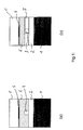
- FIG 2 is shown the case of an optical device optimized to act as a phase modulator.
- the liquid crystal (molecules 62a) along the segment of the optical waveguide shows a liquid crystal director in absence of external field to be parallel to the optical axis of said optical waveguide.
- the molecules 63a are orientated parallel to the optical waveguide. Without a voltage, the index ellipsoid has the same direction parallel to the waveguide.
- the index ellipsoid is almost isotropic (n TM ⁇ n TE ).
- n TM ⁇ n TE When the external field is applied, it will act on said liquid crystal by tilting its liquid crystal director along a plane parallel to said optical axis.
- the molecules 62b rotate due to the electric field. Essentially only the refractive index for the TM-polarized light is changed, the index ellipsoid becoming more elongated on that direction (n TM >n TE ).
- FIG. 3 A second configuration regarding the orientation of the liquid crystal is shown on figure 3 where the LC molecules 63a have a liquid crystal director in absence of external field to be perpendicular to the optical waveguide. This is more adapted for an optical device acting as a controllable waveplate. In this case, the waveguide birefringence is becoming larger. When the external field is applied, it will act on said liquid crystal by tilting the molecules 63b i.e. its liquid crystal director along a plane perpendicular to said optical axis. The orientation of the LC molecules and in this way the orientation of the waveplate can be controlled by the voltage.
- the length of the segment from the optical waveguide where the core is surrounded by the LC is defined according to the polarization control to be performed with it on an optical signal (e.g. its center wavelength) to be transmitted through said optical waveguide.
- This length defined respective to the optical signal (center wavelength) will fixe the property (modification ratio on that center wavelength) of the corresponding wave plate.
- a polarisation independent phase modulator can be realized by combining two phase modulators with a half waveplate in between. Because the cladding is removed only at the sections where phase modulation or polarization rotation is required, this concept can take advantage of the low loss and small birefringence waveguides on one hand and on the strong refractive index changes in the LC section on the other hand.
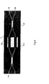
- the LC phase shifter should be more compact than the thermo-optic phase shifter. An example not restrictive is shown on figure 4.
- the PLC platform 10 includes several waveguides, four 11a, 11b, 11c, 11d for a first splitter 12 and four 13a, 13b, 13c, 13d for a second splitter 14. Between these two power splitters 12 and 14 acting e.g. as multi mode interference coupler at 3dB are structured two segments 44a and 44b from the optical waveguide connecting respectively 11c with 13a and 11d with 13b according to the present invention. These two segments 44a and 44b are obtained by etching the cladding 6 surrounding the respective cores of the optical waveguides and then filling them with LC. In such a way, a compact integrated optical switch is realized by the integration of the LC phase shifter in a PLC Mach-Zehnder amplitude modulator with ultra low power consumption.
Landscapes
- Physics & Mathematics (AREA)
- Nonlinear Science (AREA)
- Chemical & Material Sciences (AREA)
- Crystallography & Structural Chemistry (AREA)
- General Physics & Mathematics (AREA)
- Optics & Photonics (AREA)
- Optical Integrated Circuits (AREA)
- Optical Modulation, Optical Deflection, Nonlinear Optics, Optical Demodulation, Optical Logic Elements (AREA)
- Liquid Crystal (AREA)
Abstract
An inclusion of liquid crystal in the direct vicinity of the core of an optical waveguide structured on a substrate allows to build a tunable optical device. The liquid crystal will replace part of the cladding material of that integrated structure. The tuning of the optical property of that liquid crystal, i.e. its refractive index, will influence directly the mode index of the core. This influence can be of such amount to allow the control the flow of optical signals transmitted through it. The tuning is advantageously achieved by applying an electric field via electrodes to the liquid crystals. <IMAGE>
Description
This invention relates to an optical device comprising at least an optical
waveguide core for the transmission of optical signals. Such kind of optical devices
possibly made as integrated optical circuits are particularly developed for
telecommunications systems especially for a wavelength division multiplexing
communication system.
A phase modulator or shifter is a basic building block in a large variety of integrated
circuits or Planar Lightwave Devices PLD. It is about a set up allowing to
act on a controlled way on some phases of optical signals. This is achieved by a
controlled change of the refractive index through which these optical signals are
transmitted. Usually, this change is performed on an optical waveguide using
electro-optical or thermo-optical effects.
Electro-optical phase modulators are polarization dependent and require high
voltage or long waveguide structures. This implies a too high optical losses. Furthermore,
the electro-optic effect is limited to a few materials, which are more
expensive than SiO2 used usually in this field. Moreover, it is difficult to build up
very compact devices. Thermo-optic phase modulators are realized by depositing
thin film heaters on the cladding. They are not very reliable or too expensive due
to the fact that such devices consume a high electrical power. They need a typical
switching power of 0.5W. This power can be reduced by a factor of up to 10 by
etching the cladding and buffer besides the optical waveguide, using high index
contrast waveguide and thick buffer layer below the waveguide. But, this makes
the fabrication process of the phase modulator more complicated. It is necessary
for some integrated optical circuits to use a certain number of such phase shifter
either in cascade (e.g. Polarization Moden Dispersion PMD compensator) or in
parallel (e.g. Variable Optical Attenuator VOA array) where the flow of optical
signals can be controlled. In such cases, the power consumption of the whole
circuit is rising to several Watts or even more.
Another function of such phase shifter is the so-called wave plate. It is based on
a high anisotropy of the mode index of the optical waveguide along a segment
implying a differentiate influence on the different components from an optical
signal transmitted through it. The length of that segment is chosen according to
the wavelength of the optical signal to be treated and to the wished effect e.g. an
half or quarter wave plate for the rotation respectively about 180° or 90° of the
corresponding polarization vector. Wave plate on PLD are realized by cutting a
trench through the waveguide and inserting a film like polymide. Such wave
plates are not tunable and suffer from radiation losses. The insertion of such a
film is not adapted to mass production.
Also known are mechanical influences on fibers by stretching it. The physical size
of its core is changed along a segment allowing a more or less controlled modification
of some phases from optical signals transmitted through it (fiber strechers
are phase shifters - stress along the fibre - as well as waveplates - stress perpendicular
to it -). An alternative also based on the use of a fiber is described in
the article from EI-Sherif et al. published in SPIE 722, 59 (1986). It consists by
replacing the passive cladding material on a small part of the fiber core by an
active one. This is obtained using a nematic liquid crystal as an active clad material
of a multimode fiber over a short length. If the index of the cladding and the
modified cladding are matched, the device will exhibit no insertion loss. When an
external electric field is applied to this electro-optical material, the index of the
modified cladding changes, leading to new boundary conditions for the light
propagated inside the fiber.
In US 6,154,591 is described a tunable optical device comprising a substrate
and a superstrate such that first and second optical waveguides are sandwiched
between said substrate and said superstrate so as to define a space between said
waveguides. This space is adapted to act as an optical resonant cavity by filling it
with a liquid crystal material to permit to tune said cavity. This is obtained by
some alignment means disposed on at least one of the substrate and the superstrate
such that the liquid crystal are orientated to respond to an applied electric
field.
A liquid crystal phase modulator can be used in all applications where the polarization
dependence is not crucial or is evaded by polarization splitting. If the
phase modulator is integrated in a Mach-Zehnder waveguide interferometer, an
amplitude modulator is realized (e.g. array of 40 variable optical attenuators
consuming very low power). Dispersion equalizers and polarization mode dispersion
compensators are typical application due to the usual requirement of a
whole series of phase modulators. The phase shifters are especially suited for
the PMD compensator where phase shifting is performed only in one polarization.
Phase modulation is required in tunable integrated optical filters. There is a
strong demand for tunable filters with low power consumption particularly in
metro and in access optical network. The integration of thermo-optical phase
shifters with temperature sensitive devices (e.g. array waveguide grating, AWG) is
difficult, because local heating leads to an increase of the chip temperature. Liquid
crystal phase shifters allow this integration since nearly no electrical power is
needed for the liquid crystal phase modulator. The realization of tunable waveplates
allows the development of an integrated optical polarization controller.
Moreover, the integration of a lambda half plate in the middle of an integrated
optical chip can be used to realize polarization independent devices. Normally,
the polarization dependence due to the anisotropy structure of the liquid crystal
molecules induces a strong birefringence. With the combination of the half
waveplate with two polarization dependent phase modulators, a polarization
independent phase modulator can be realized.
But, it is very difficult to integrate the liquid crystals on planar lightwave circuits
because they can not be structured using photolithography to obtain waveguides.
Moreover, the optical losses essentially on the transition from the passive
waveguide to the active waveguide as described in US 6,154,591 are too large
(in the order of dB/cm).
It is an object of the present invention to achieve an optical device with a segment
showing a reversible high index change along the transmission of optical
signals without implying high power consumption. Furthermore, it is an aim to
develop such kind of optical device while being relatively cheap to manufacture.
Advantageously, an inclusion of the liquid crystal in the direct vicinity of the core
of an optical waveguide structured on a substrate allows to build a tunable optical
device. The liquid crystal will be confined by replacing cladding material of
that integrated structure. The tuning of the property of that liquid crystal i.e. its
refractive index will influence directly the mode index of the core. This influence
can be of such amount to allow to control the flow of optical signals transmitted
through it. The tuning is advantageously achieved by applying some electric field
via electrode on a segment of that core confined with liquid crystals.
According to the choice of the configuration for the molecules building up the
liquid crystal i.e. the choice of the liquid crystal director respective to the optical
axis, it is possible to realize different tunable devices. Therefore, a phase modulator
or controllable wave plate or even a combination of both can be developed
following the present invention.
Further advantageous features of the invention are defined in the dependent
claims and will become apparent from the following description and the drawings.
One embodiment of the invention will now be explained in more detail with reference
to the accompanying drawings, in which:
On figures 1 a and 1b are shown a cross section of two configurations of an optical
device according to the present invention. The core 3 of an optical waveguide
is structured as usual using e.g. photolitography on some buffer 2 (e.g. made out
of SiO2-material) itself grown on some substrate (e.g. made out of Si-material).
The present invention consists by substituting the standard waveguide cladding 7
(e.g. SiO2) surrounding the core 3 by some Liquid Crystal LC 6. This is performed
on the three sides - fig. 1a - or only on the top or upper side - fig 1 b - along a
defined segment of that core 3. Above the LC 6 are placed some electrodes e.g.
by etching process. The whole is covered by some glass 5 as a protection and a
supplementary confinement.
This build two basic configurations are possible. On figure 1a the cladding is
completely substituted by the LC. The second configuration shown on fig. 1b is
advantageous for the integration in standard planar lightwave circuit
waveguides. They can be fabricated as follow: after fabricating the standard PLC
platform a part of the cladding 2 is removed by (RIE) etching. The liquid crystal is
filled 6 and orientated. Afterwards a glass substrate 5 with the upper electrodes 4
is fixed on the top. The configuration of fig. 1b requires a more complicated
etching process. The upper electrode 4 is mounted together with the glass cover
5 above the LC 6. For both cases, it is the buffer 1 (Si) which is also used as the
lower electrode.
The mode index is changed by the change of the refractive index of the cladding
material substituted now at least partly with LC. The influence of this change can
be adjusted by the waveguide design. For instance, a decrease of the waveguide
width leads to an enlarged mode field with a higher field amplitude in the cladding
material. If a smaller variation of the mode index is required broader
waveguides can be used and the standard SiO2-cladding should take a larger
part of the waveguide surrounding (see configuration shown on fig. 1b). The
effect of the LC can be also reduced by performing the etching step not up to top
of the core but leaving some thin SiO2 cladding layer above the waveguide.
The two different applications i.e. phase modulator and controllable waveplate
can be realized by a different orientations of the LC molecules 62a, 62b, 63a,
63b (liquid crystal director). On figure 2 is shown the case of an optical device
optimized to act as a phase modulator. The liquid crystal (molecules 62a) along
the segment of the optical waveguide shows a liquid crystal director in absence
of external field to be parallel to the optical axis of said optical waveguide. The
molecules 63a are orientated parallel to the optical waveguide. Without a voltage,
the index ellipsoid has the same direction parallel to the waveguide. So,
birefringence B (=nTM-nTE, with nTM and nTE the refractive index respectively for the
TM and TE components of an optical signal vector at a specific wavelength) is
small. The index ellipsoid is almost isotropic (nTM≈nTE). When the external field is
applied, it will act on said liquid crystal by tilting its liquid crystal director along a
plane parallel to said optical axis. The molecules 62b rotate due to the electric
field. Essentially only the refractive index for the TM-polarized light is changed,
the index ellipsoid becoming more elongated on that direction (nTM>nTE).
A second configuration regarding the orientation of the liquid crystal is shown on
figure 3 where the LC molecules 63a have a liquid crystal director in absence of
external field to be perpendicular to the optical waveguide. This is more adapted
for an optical device acting as a controllable waveplate. In this case, the
waveguide birefringence is becoming larger. When the external field is applied, it
will act on said liquid crystal by tilting the molecules 63b i.e. its liquid crystal director
along a plane perpendicular to said optical axis. The orientation of the LC
molecules and in this way the orientation of the waveplate can be controlled by
the voltage.
The length of the segment from the optical waveguide where the core is surrounded
by the LC is defined according to the polarization control to be performed
with it on an optical signal (e.g. its center wavelength) to be transmitted
through said optical waveguide. This length defined respective to the optical signal
(center wavelength) will fixe the property (modification ratio on that center
wavelength) of the corresponding wave plate. With the right waveguide length,
quarter waveplates and half waveplates can be realized and combined to a fully
polarization controller.
Even a polarisation independent phase modulator can be realized by combining
two phase modulators with a half waveplate in between. Because the cladding is
removed only at the sections where phase modulation or polarization rotation is
required, this concept can take advantage of the low loss and small birefringence
waveguides on one hand and on the strong refractive index changes in the LC
section on the other hand. The LC phase shifter should be more compact than
the thermo-optic phase shifter. An example not restrictive is shown on figure 4.
The PLC platform 10 includes several waveguides, four 11a, 11b, 11c, 11d for a
first splitter 12 and four 13a, 13b, 13c, 13d for a second splitter 14. Between
these two power splitters 12 and 14 acting e.g. as multi mode interference coupler
at 3dB are structured two segments 44a and 44b from the optical
waveguide connecting respectively 11c with 13a and 11d with 13b according to
the present invention. These two segments 44a and 44b are obtained by etching
the cladding 6 surrounding the respective cores of the optical waveguides and
then filling them with LC. In such a way, a compact integrated optical switch is
realized by the integration of the LC phase shifter in a PLC Mach-Zehnder amplitude
modulator with ultra low power consumption.
The integration of ferroelectric kind of liquid crystal i.e. made of twisted nematic
liquid crystal molecules, will give the possibility to build even faster modulators
(<100µs) than thermooptical ones. And optical devices according to the present
invention like LC waveplate are much better adapted for mass production.
Claims (15)
- An optical device comprising at least an optical waveguide core structured on a substrate and showing a mode index defined according to the refractive index of its surrounding characterized in, that said optical waveguide core is surrounded along a segment at least partly by some liquid crystal material with a refractive index tunable by applying on it some external field.
- An optical device according to claim 1, characterized in, that it comprises some electrode on the vicinity of said liquid crystal material for the generation of said external field as an electrical field.
- An optical device according to claim 1, characterized in, that along said segment said liquid crystal material is only on top of said optical waveguide core, while the other sides of said optical waveguide core being surrounded by another cladding material.
- An optical device according to claim 1, characterized in, that said liquid crystal along said segment shows a liquid crystal director in absence of external field to be parallel to the optical axis of said optical waveguide.
- An optical device according to claim 4, characterized in, that said external field when applied will act on said liquid crystal by tilting its liquid crystal director along a plane parallel to said optical axis.
- An optical device according to claim 5, characterized in, that said segment is used as a phase modulator for optical signals to be transmitted through said optical waveguide.
- An optical device according to claim 1, characterized in, that said liquid crystal along said segment shows a liquid crystal director in absence of external field to be perpendicular to said optical waveguide.
- An optical device according to claim 7, characterized in, that said external field when applied will act on said liquid crystal by tilting its liquid crystal director along a plane perpendicular to said optical axis.
- An optical device according to claim 8, characterized in, that the length of said segment is defined according to the polarization control to be performed with it on an optical signal to be transmitted through said optical waveguide.
- An optical device according to claim 9, characterized in, that said segment is used as a waveplate of specific ratio defined in relation to said optical signal.
- An optical device according to claim 1, characterized in, that said optical waveguide core shows a combination of several segments defined according to claim 6 and 10.
- An optical device according to claim 11, characterized in, that said combination consists of two segments acting as phase modulator with in between a segment acting as a waveplate.
- An optical device according to claim 12, characterized in, that said combination is polarization independent at least for some optical signal to be transmitted through said optical waveguide.
- An optical device according to claim 1, characterized in, that said liquid crystal is made out of some ferroelectric liquid crystal.
- An optical device according to claim 1, characterized in, that said segment is at least part of a phase shifter from an integrated optical circuit.
Priority Applications (2)
| Application Number | Priority Date | Filing Date | Title |
|---|---|---|---|
| EP02360172A EP1372024A1 (en) | 2002-06-12 | 2002-06-12 | Liquid crystal optical phase modulator |
| US10/446,666 US20030231279A1 (en) | 2002-06-12 | 2003-05-29 | Liquid crystal phase modulator on integrated optical circuit |
Applications Claiming Priority (1)
| Application Number | Priority Date | Filing Date | Title |
|---|---|---|---|
| EP02360172A EP1372024A1 (en) | 2002-06-12 | 2002-06-12 | Liquid crystal optical phase modulator |
Publications (1)
| Publication Number | Publication Date |
|---|---|
| EP1372024A1 true EP1372024A1 (en) | 2003-12-17 |
Family
ID=29558450
Family Applications (1)
| Application Number | Title | Priority Date | Filing Date |
|---|---|---|---|
| EP02360172A Withdrawn EP1372024A1 (en) | 2002-06-12 | 2002-06-12 | Liquid crystal optical phase modulator |
Country Status (2)
| Country | Link |
|---|---|
| US (1) | US20030231279A1 (en) |
| EP (1) | EP1372024A1 (en) |
Families Citing this family (14)
| Publication number | Priority date | Publication date | Assignee | Title |
|---|---|---|---|---|
| JP2005128419A (en) * | 2003-10-27 | 2005-05-19 | Nec Corp | Optical waveguide structure and its manufacturing method |
| US8860897B1 (en) | 2004-01-22 | 2014-10-14 | Vescent Photonics, Inc. | Liquid crystal waveguide having electric field orientated for controlling light |
| US8989523B2 (en) | 2004-01-22 | 2015-03-24 | Vescent Photonics, Inc. | Liquid crystal waveguide for dynamically controlling polarized light |
| US20050271325A1 (en) * | 2004-01-22 | 2005-12-08 | Anderson Michael H | Liquid crystal waveguide having refractive shapes for dynamically controlling light |
| US8463080B1 (en) | 2004-01-22 | 2013-06-11 | Vescent Photonics, Inc. | Liquid crystal waveguide having two or more control voltages for controlling polarized light |
| GB0507012D0 (en) * | 2005-04-06 | 2005-05-11 | Univ Southampton | A tunable filter device comprising a waveguide, a bragg grating, and a planar substrate |
| US7570320B1 (en) * | 2005-09-01 | 2009-08-04 | Vescent Photonics, Inc. | Thermo-optic liquid crystal waveguides |
| US7783144B2 (en) | 2006-04-24 | 2010-08-24 | The Hong Kong University Of Science And Technology | Electrically tunable microresonators using photoaligned liquid crystals |
| US9366938B1 (en) | 2009-02-17 | 2016-06-14 | Vescent Photonics, Inc. | Electro-optic beam deflector device |
| US8995038B1 (en) | 2010-07-06 | 2015-03-31 | Vescent Photonics, Inc. | Optical time delay control device |
| US8442078B1 (en) * | 2011-12-12 | 2013-05-14 | Massachusetts Institute Of Technology | Microfluidic radial fiber laser utilizing an external polarizer to modulate its azimuthal intensity distribution |
| US10048518B2 (en) * | 2013-03-19 | 2018-08-14 | Luxtera, Inc. | Method and system for a low-voltage integrated silicon high-speed modulator |
| US9541775B2 (en) * | 2013-03-19 | 2017-01-10 | Luxtera, Inc. | Method and system for a low-voltage integrated silicon high-speed modulator |
| US10976579B2 (en) | 2018-08-09 | 2021-04-13 | Analog Devices, Inc. | Liquid crystal waveguide with active incoupling |
Citations (6)
| Publication number | Priority date | Publication date | Assignee | Title |
|---|---|---|---|---|
| US3802760A (en) * | 1971-06-29 | 1974-04-09 | Bell Telephone Labor Inc | Devices for varying thin film waveguiding properties |
| GB1536518A (en) * | 1977-08-04 | 1978-12-20 | Standard Telephones Cables Ltd | Tap arrangement for a fibre optic transmission system |
| US4721352A (en) * | 1986-02-26 | 1988-01-26 | The Board Of Trustees Of The Leland Stanford Junior University | Polarizing apparatus and method utilizing an optical fiber |
| US5044712A (en) * | 1990-06-29 | 1991-09-03 | The United States Of America As Represented By The Secretary Of The Air Force | Waveguided electrooptic switches using ferroelectric liquid crystals |
| US5388169A (en) * | 1993-04-26 | 1995-02-07 | Tokyo University Of Agriculture And Technology | Optical waveguide type synaptic weight modulator with nematic liquid crystal cladding |
| JP2000221343A (en) * | 1999-01-28 | 2000-08-11 | Toshiba Corp | Optical tunable filter |
Family Cites Families (1)
| Publication number | Priority date | Publication date | Assignee | Title |
|---|---|---|---|---|
| US6154591A (en) * | 1998-04-20 | 2000-11-28 | British Telecommunications Public Limited Company | Tunable optical device |
-
2002
- 2002-06-12 EP EP02360172A patent/EP1372024A1/en not_active Withdrawn
-
2003
- 2003-05-29 US US10/446,666 patent/US20030231279A1/en not_active Abandoned
Patent Citations (6)
| Publication number | Priority date | Publication date | Assignee | Title |
|---|---|---|---|---|
| US3802760A (en) * | 1971-06-29 | 1974-04-09 | Bell Telephone Labor Inc | Devices for varying thin film waveguiding properties |
| GB1536518A (en) * | 1977-08-04 | 1978-12-20 | Standard Telephones Cables Ltd | Tap arrangement for a fibre optic transmission system |
| US4721352A (en) * | 1986-02-26 | 1988-01-26 | The Board Of Trustees Of The Leland Stanford Junior University | Polarizing apparatus and method utilizing an optical fiber |
| US5044712A (en) * | 1990-06-29 | 1991-09-03 | The United States Of America As Represented By The Secretary Of The Air Force | Waveguided electrooptic switches using ferroelectric liquid crystals |
| US5388169A (en) * | 1993-04-26 | 1995-02-07 | Tokyo University Of Agriculture And Technology | Optical waveguide type synaptic weight modulator with nematic liquid crystal cladding |
| JP2000221343A (en) * | 1999-01-28 | 2000-08-11 | Toshiba Corp | Optical tunable filter |
Non-Patent Citations (2)
| Title |
|---|
| HERMANN D S ET AL: "Electro-optic modulation of light by a planar waveguide based on ferroelectric liquid crystals", 5TH EUROPEAN CONFERENCE ON LIQUID CRYSTALS (ECLC 99), HERSONISSOS, GREECE, 25-30 APRIL 1999, vol. 352, Molecular Crystals and Liquid Crystals, 2000, Gordon & Breach, Switzerland, pages 379 - 388, XP002226889, ISSN: 1058-725X * |
| PATENT ABSTRACTS OF JAPAN vol. 2000, no. 11 3 January 2001 (2001-01-03) * |
Also Published As
| Publication number | Publication date |
|---|---|
| US20030231279A1 (en) | 2003-12-18 |
Similar Documents
| Publication | Publication Date | Title |
|---|---|---|
| Voges et al. | Integrated-optic devices on LiNbO 3 for optical communication | |
| Eldada | Optical communication components | |
| Jinguji et al. | Two-port optical wavelength circuits composed of cascaded Mach-Zehnder interferometers with point-symmetrical configurations | |
| US6853758B2 (en) | Scheme for controlling polarization in waveguides | |
| US7155088B2 (en) | Optical modulator and optical modulator array | |
| Eldada | Polymer integrated optics: promise versus practicality | |
| Alferness | Titanium-diffused lithium niobate waveguide devices | |
| US6859567B2 (en) | In-guide control of optical propagation | |
| CN101672987B (en) | Optical isolator, optical add/drop multiplexer and optical combiner | |
| EP1279999A1 (en) | Polarization-insensitive variable optical attenuator | |
| EP1372024A1 (en) | Liquid crystal optical phase modulator | |
| EP0540088B1 (en) | Integrated optical component | |
| US20020159684A1 (en) | Novel optical waveguide switch using cascaded mach-zehnder interferometers | |
| CN113534504A (en) | Electric control adjustable polarization beam splitting method and device based on thin-film lithium niobate | |
| JP2006506688A (en) | Waveguide device with optical functional medium based on Kerr effect | |
| Wang et al. | Low-power and wide-band 1× 8 silica waveguide optical switch | |
| US6904207B2 (en) | Waveguide type liquid-crystal optical switch | |
| Kato et al. | Switching operation in tunable add-drop multiplexer with si-grating waveguides featuring ferroelectric liquid crystal cladding | |
| US20020159702A1 (en) | Optical mach-zehnder interferometers with low polarization dependence | |
| US7010198B2 (en) | Birefringence trimming of integrated optical devices by elevated heating | |
| Kitoh et al. | Novel broad-band optical switch using silica-based planar lightwave circuit | |
| EP1159647A1 (en) | Directional coupler type electro-optic modulator | |
| US20030039447A1 (en) | Strip-loaded optical waveguide | |
| Dupont et al. | Principle of a compact polarisation mode dispersion controller using homeotropic electroclinic liquid crystal confined single mode fibre devices | |
| Sirleto et al. | Optical multimode interference router based on a liquid crystal waveguide |
Legal Events
| Date | Code | Title | Description |
|---|---|---|---|
| PUAI | Public reference made under article 153(3) epc to a published international application that has entered the european phase |
Free format text: ORIGINAL CODE: 0009012 |
|
| AK | Designated contracting states |
Kind code of ref document: A1 Designated state(s): AT BE CH CY DE DK ES FI FR GB GR IE IT LI LU MC NL PT SE TR |
|
| AX | Request for extension of the european patent |
Extension state: AL LT LV MK RO SI |
|
| RAP1 | Party data changed (applicant data changed or rights of an application transferred) |
Owner name: AVANEX CORPORATION |
|
| STAA | Information on the status of an ep patent application or granted ep patent |
Free format text: STATUS: THE APPLICATION HAS BEEN WITHDRAWN |
|
| 17P | Request for examination filed |
Effective date: 20040601 |
|
| 18W | Application withdrawn |
Effective date: 20040609 |