EP1370015A2 - Optical signal generator and method thereof - Google Patents
Optical signal generator and method thereof Download PDFInfo
- Publication number
- EP1370015A2 EP1370015A2 EP03010829A EP03010829A EP1370015A2 EP 1370015 A2 EP1370015 A2 EP 1370015A2 EP 03010829 A EP03010829 A EP 03010829A EP 03010829 A EP03010829 A EP 03010829A EP 1370015 A2 EP1370015 A2 EP 1370015A2
- Authority
- EP
- European Patent Office
- Prior art keywords
- optical
- phase
- modulator
- data
- sideband
- Prior art date
- Legal status (The legal status is an assumption and is not a legal conclusion. Google has not performed a legal analysis and makes no representation as to the accuracy of the status listed.)
- Withdrawn
Links
Images






Classifications
-
- H—ELECTRICITY
- H04—ELECTRIC COMMUNICATION TECHNIQUE
- H04B—TRANSMISSION
- H04B10/00—Transmission systems employing electromagnetic waves other than radio-waves, e.g. infrared, visible or ultraviolet light, or employing corpuscular radiation, e.g. quantum communication
- H04B10/50—Transmitters
- H04B10/516—Details of coding or modulation
- H04B10/548—Phase or frequency modulation
-
- H—ELECTRICITY
- H04—ELECTRIC COMMUNICATION TECHNIQUE
- H04B—TRANSMISSION
- H04B10/00—Transmission systems employing electromagnetic waves other than radio-waves, e.g. infrared, visible or ultraviolet light, or employing corpuscular radiation, e.g. quantum communication
- H04B10/50—Transmitters
- H04B10/501—Structural aspects
- H04B10/503—Laser transmitters
- H04B10/505—Laser transmitters using external modulation
-
- H—ELECTRICITY
- H04—ELECTRIC COMMUNICATION TECHNIQUE
- H04B—TRANSMISSION
- H04B10/00—Transmission systems employing electromagnetic waves other than radio-waves, e.g. infrared, visible or ultraviolet light, or employing corpuscular radiation, e.g. quantum communication
- H04B10/50—Transmitters
- H04B10/501—Structural aspects
- H04B10/503—Laser transmitters
- H04B10/505—Laser transmitters using external modulation
- H04B10/5051—Laser transmitters using external modulation using a series, i.e. cascade, combination of modulators
-
- H—ELECTRICITY
- H04—ELECTRIC COMMUNICATION TECHNIQUE
- H04B—TRANSMISSION
- H04B10/00—Transmission systems employing electromagnetic waves other than radio-waves, e.g. infrared, visible or ultraviolet light, or employing corpuscular radiation, e.g. quantum communication
- H04B10/50—Transmitters
- H04B10/516—Details of coding or modulation
- H04B10/5165—Carrier suppressed; Single sideband; Double sideband or vestigial
Definitions
- This invention generally relates to an optical signal generator and method thereof and more specifically relates to an optical signal generator and method thereof to generate a vestigial sideband (VSB) modulated optical signal.
- VSB vestigial sideband
- phase modulation method As typical methods to generate a VSB or SSB optical signal, there is a method to emphasize one of sidebands using phase modulation (hereinafter, referred as a phase modulation method) and a method to remove unnecessary band components with an optical filter (e.g. an interleaver) (hereinafter, referred as an optical filter method).
- an optical filter method e.g. an interleaver
- phase modulation method when one of sidebands is emphasized through phase modulation, harmonic components located outside the sideband are also emphasized. As a result, crosstalk between adjacent wavelengths increases causing deterioration of the transmission characteristics.
- An object of the invention is to provide an optical signal generator and method thereof to generate an optical signal with little crosstalk between adjacent wavelengths and an optical pulse width which does not expand.
- An optical signal generator comprises a light source to generate an optical carrier, a data modulator to modulate the optical carrier output from the light source with a transmission data, an optical phase modulator to modulate an optical phase of an output light from the data modulator in synchronization with the output light from the data modulator so as to emphasize one of sidebands, and an optical filter to remove harmonic components located outside the emphasized sideband out of an output light from the optical phase modulator.
- An optical signal generating method comprises steps of generating a data modulated light by modulating an optical carrier with a transmission data, emphasizing one of sidebands by modulating an optical phase of the data modulated light, and removing harmonic components located outside the emphasized sideband.
- FIG. 1 shows a schematic block diagram of an embodiment according to the invention.
- a data generator 10 generates a transmission data having pulses of 50% duty ratio according to a clock output from a clock generator 12.
- a light source 14 generates a laser light to become an optical carrier for carrying the transmission data output from the data generator 10 and applies the laser light to a data modulator 16.
- the data modulator 16 intensity-modulates the laser light from the light source 14 with the transmission data from the data generator 10 to generate an optical signal of RZ optical pulse train for carrying the transmission data.
- the generated optical pulse train is applied to a phase modulator 18.
- a sine wave generator 20 according to the clock output from the clock generator 12, generates a sine wave signal synchronizing with the clock and having a frequency identical with a frequency of the clock.
- a phase shifter 22 shifts a phase of the sine wave signal output from the sine wave generator 20 by ⁇ /2 and applies the sine wave signal to the phase modulator 16.
- the phase modulator 18 modulates an optical phase of each optical pulse in the optical pulse train from the data modulator 16 with the sine wave signal from the phase shifter 22.
- the phase-modulated optical pulse train is sent into an optical fiber transmission line through an optical filter 24 which removes harmonic components emphasized by the phase modulator 18.
- phase modulation has been applied to a signal light beforehand in order to suppress self phase modulation due to a nonlinear effect of an optical fiber.
- a phase relation between an optical pulse and a modulating signal for phase modulation is that a sine wave signal reaches one extreme value at the rise timing of the optical pulse and reaches the other extreme value at the fall timing of the optical pulse.
- the phase relation is such that the polarity of the modulating signal changes in the center part of the optical pulse.
- a modulating signal (a driving signal of a phase modulator) is in-phase (a phase difference 0) or opposite-phase (a phase difference ⁇ ) .
- reference numeral 30 denotes an optical pulse to be phase-modulated
- 32 denotes an in-phase modulating signal
- 34 denotes an opposite-phase modulating signal respectively.
- a phase shifter 22 shifts a phase of the sine wave signal by + ⁇ /2 or - ⁇ /2 before applying the sine wave signal as a modulating signal (a driving signal) to the phase modulator 18.
- Fig. 3 shows a waveform timing chart in the phase modulator 18 according to the embodiment.
- Reference numeral 40 denotes an optical pulse applied to the phase modulator 18 from the data modulator 16
- 42 denotes a modulating signal (a driving signal) with phase shifting amount ⁇ /2 applied to the phase modulator 18 from the phase shifter 22
- 44 denotes a modulating signal (a driving signal) with phase shifting amount - ⁇ /2 applied to the phase modulator 18 from the phase shifter 22 respectively.
- the phase shifting amount in the phase shifter 22 is described as ⁇ /2 or - ⁇ /2, for explanatory convenience, this amount is practically the phase difference between the optical pulse and the modulating signal in the phase modulator 18.
- Fig. 5 shows a spectrum obtained by applying the embodiment to an optical pulse having a spectrum shown in Fig. 4. Obviously from Fig. 5, one sideband is emphasized and the other is suppressed.
- a solution for overcoming the deterioration of transmission characteristics is to employ a method to decrease the accumulated chromatic dispersion by cutting down the transmission distance or/and a method to decrease the accumulated chromatic. dispersion by utilizing a fiber (a dispersion management fiber) with a combination for flattening a dispersion slope. When the latter method is employed, this embodiment is applicable to long haul transmission as well.
- Fig. 6 shows a spectrum diagram of phase difference 0 (prior art)
- Fig. 7 shows a spectrum diagram of phase difference - ⁇ /4
- Fig. 8 shows a spectrum diagram of phase difference - ⁇ /2
- Fig. 9 shows a spectrum diagram of phase difference -3 ⁇ /4
- Fig. 10 shows a spectrum diagram of phase difference - ⁇ (prior art) respectively.
- phase difference in the phase modulator 18 gives to the transmission characteristics using, for example, a WDM signal with a wavelength interval 0.15 nm is measured.
- the result is shown in Fig. 11.
- the horizontal axis shows the phase difference in the phase modulator 18, and the vertical axis shows a penalty for the Q value at the phase difference - ⁇ /2.
- the wavelength interval 0.15 nm if the phase difference is set to 0 or ⁇ , it is impossible to measure the Q value because overlapping of wavelengths with next wavelengths reaches to the point not to be negligible. As understandable from Fig.
- phase difference between the optical pulse and the modulating signal is set to ⁇ /2 or - ⁇ /2, even it is set to within a range of ⁇ /2- ⁇ /4 to ⁇ /2+ ⁇ /4 or - ⁇ /2- ⁇ /4 to - ⁇ /2+ ⁇ /4, a satisfactory Q value is obtained.
- the optical filter 24 removes harmonic components located outside the sideband emphasized by the phase modulator 18.
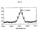
- Fig. 12 shows a spectrum of an output light from the data modulator 16
- Fig. 13 shows a spectrum of an output light from the phase modulator 18
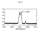
- Fig. 14 shows a spectrum of an output light from the optical filter 24.
- the optical filter 24 can comprise an optical filter to remove the harmonic components outside the sideband emphasized by the phase modulator 18 as described above, it also can be an optical bandpass filter to transmit exclusively the carrier and sideband emphasized by the phase modulator 18.
- Fig. 14 shows a spectrum of the latter case.
- VSB modulated signal lights having satisfactory transmission characteristics are generated with a very simple configuration.
Landscapes
- Physics & Mathematics (AREA)
- Electromagnetism (AREA)
- Engineering & Computer Science (AREA)
- Computer Networks & Wireless Communication (AREA)
- Signal Processing (AREA)
- Optics & Photonics (AREA)
- Optical Communication System (AREA)
- Optical Modulation, Optical Deflection, Nonlinear Optics, Optical Demodulation, Optical Logic Elements (AREA)
Abstract
Description
- This invention generally relates to an optical signal generator and method thereof and more specifically relates to an optical signal generator and method thereof to generate a vestigial sideband (VSB) modulated optical signal.
- With the advance of wavelength division multiplexing transmission technology, a transmission capacity of an optical fiber has been increasing. However, in a general optical modulation system (both-sideband (BSB) modulation), the number of optical signal wavelengths to be crammed in a limited band space is limited. As a method to make wavelength intervals narrower, systems to use single sideband (SSB) modulation and vestigial sideband (VSB) modulation have been studied (e.g. "LiNbO3 Optical Single-Sideband Modulator", Electronics OFC2000PD16, and "10 Gbit/s optical signal sideband system", Electronics Letters vol. 33, No. 11, pp. 970-973, 22nd May 1977).
- As typical methods to generate a VSB or SSB optical signal, there is a method to emphasize one of sidebands using phase modulation (hereinafter, referred as a phase modulation method) and a method to remove unnecessary band components with an optical filter (e.g. an interleaver) (hereinafter, referred as an optical filter method).
- In the phase modulation method, when one of sidebands is emphasized through phase modulation, harmonic components located outside the sideband are also emphasized. As a result, crosstalk between adjacent wavelengths increases causing deterioration of the transmission characteristics.
- In the optical filter method, since signal components are removed by an optical filter, an optical pulse width in the time domain becomes wider. Accordingly, it is difficult to increase a bit rate.
- An object of the invention is to provide an optical signal generator and method thereof to generate an optical signal with little crosstalk between adjacent wavelengths and an optical pulse width which does not expand.
- An optical signal generator according to the invention comprises a light source to generate an optical carrier, a data modulator to modulate the optical carrier output from the light source with a transmission data, an optical phase modulator to modulate an optical phase of an output light from the data modulator in synchronization with the output light from the data modulator so as to emphasize one of sidebands, and an optical filter to remove harmonic components located outside the emphasized sideband out of an output light from the optical phase modulator.
- An optical signal generating method according to the invention comprises steps of generating a data modulated light by modulating an optical carrier with a transmission data, emphasizing one of sidebands by modulating an optical phase of the data modulated light, and removing harmonic components located outside the emphasized sideband.
- The above and other objects, features and advantages of the present invention will be apparent from the following detailed description of embodiments of the invention in conjunction with the accompanying drawings, in which:
- Fig. 1 shows a schematic block diagram of an embodiment according to the invention;
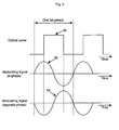
- Fig. 2 shows waveforms in conventional phase modulation;
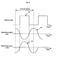
- Fig. 3 shows waveforms in phase modulation according to the embodiment;
- Fig. 4 shows a BSB spectrum example;
- Fig. 5 shows a VSB spectrum example according to the embodiment;
- Fig. 6 shows a spectrum example of a phase difference 0 (prior art);
- Fig. 7 shows a spectrum example of phase difference -π/4;
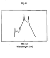
- Fig. 8 shows a spectrum example of phase difference -π/2;
- Fig. 9 shows a spectrum example of phase difference -3π/4;
- Fig. 10 shows a spectrum example of phase difference -π (prior art);
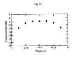
- Fig. 11 shows a measured example of Q value penalty for phase differences;
- Fig. 12 shows a spectrum example of an output light from
a
data modulator 16; - Fig. 13 shows a spectrum example of an output light from
a
phase modulator 18; and - Fig. 14 shows a spectrum example of an output light from
an
optical filter 24. -
- Embodiments of the invention are explained below in detail with reference to the drawings.
- Fig. 1 shows a schematic block diagram of an embodiment according to the invention. A
data generator 10 generates a transmission data having pulses of 50% duty ratio according to a clock output from aclock generator 12. Alight source 14 generates a laser light to become an optical carrier for carrying the transmission data output from thedata generator 10 and applies the laser light to adata modulator 16. Thedata modulator 16 intensity-modulates the laser light from thelight source 14 with the transmission data from thedata generator 10 to generate an optical signal of RZ optical pulse train for carrying the transmission data. The generated optical pulse train is applied to aphase modulator 18. - On the other hand, a
sine wave generator 20, according to the clock output from theclock generator 12, generates a sine wave signal synchronizing with the clock and having a frequency identical with a frequency of the clock. Aphase shifter 22 shifts a phase of the sine wave signal output from thesine wave generator 20 by π/2 and applies the sine wave signal to thephase modulator 16. - The
phase modulator 18 modulates an optical phase of each optical pulse in the optical pulse train from thedata modulator 16 with the sine wave signal from thephase shifter 22. The phase-modulated optical pulse train is sent into an optical fiber transmission line through anoptical filter 24 which removes harmonic components emphasized by thephase modulator 18. - Generally, phase modulation has been applied to a signal light beforehand in order to suppress self phase modulation due to a nonlinear effect of an optical fiber. In this case, as shown in Fig. 2, a phase relation between an optical pulse and a modulating signal for phase modulation is that a sine wave signal reaches one extreme value at the rise timing of the optical pulse and reaches the other extreme value at the fall timing of the optical pulse. In other words, the phase relation is such that the polarity of the modulating signal changes in the center part of the optical pulse. Assuming that an optical pulse exists in the center of one bit period, a modulating signal (a driving signal of a phase modulator) is in-phase (a phase difference 0) or opposite-phase (a phase difference π) . In Fig. 2,
reference numeral 30 denotes an optical pulse to be phase-modulated, 32 denotes an in-phase modulating signal, and 34 denotes an opposite-phase modulating signal respectively. - In the embodiment, on the contrary, a
phase shifter 22 shifts a phase of the sine wave signal by +π/2 or -π/2 before applying the sine wave signal as a modulating signal (a driving signal) to thephase modulator 18. Fig. 3 shows a waveform timing chart in thephase modulator 18 according to the embodiment.Reference numeral 40 denotes an optical pulse applied to thephase modulator 18 from thedata modulator phase modulator 18 from thephase shifter phase modulator 18 from thephase shifter 22 respectively. Although the phase shifting amount in thephase shifter 22 is described as π/2 or -π/2, for explanatory convenience, this amount is practically the phase difference between the optical pulse and the modulating signal in thephase modulator 18. - When a phase of phase modulation is intentionally shifted as performed in the embodiment, one of the two signal sidebands generated through data modulation (intensity modulation) at the
data modulator 16 is emphasized and the other is suppressed. Fig. 5 shows a spectrum obtained by applying the embodiment to an optical pulse having a spectrum shown in Fig. 4. Obviously from Fig. 5, one sideband is emphasized and the other is suppressed. - Because of the phase shifting in phase modulation, the effect for negating the self phase modulation due to the nonlinear effect of optical fiber decreases and thus transmission characteristics deteriorate due to the interaction with chromatic dispersion. A solution for overcoming the deterioration of transmission characteristics, for example, is to employ a method to decrease the accumulated chromatic dispersion by cutting down the transmission distance or/and a method to decrease the accumulated chromatic. dispersion by utilizing a fiber (a dispersion management fiber) with a combination for flattening a dispersion slope. When the latter method is employed, this embodiment is applicable to long haul transmission as well.
- The effect that a phase shifting amount in the
phase shifter 22, more specifically a phase difference between the optical pulse and the modulating signal in thephase modulator 18 gives to sidebands is studied. Fig. 6 shows a spectrum diagram of phase difference 0 (prior art), Fig. 7 shows a spectrum diagram of phase difference -π/4, Fig. 8 shows a spectrum diagram of phase difference -π/2, Fig. 9 shows a spectrum diagram of phase difference -3π/4, and Fig. 10 shows a spectrum diagram of phase difference -π (prior art) respectively. As obviously from Figs. 6 to 10, when the phase difference is set to π/2 or -π/2, one of sidebands is most suppressed, and when the phase difference is set to within a range of π/2-π/4 to π/2+π/4, or -π/2-π/4 to -π/2+π/4, a satisfactory suppression effect for the sidebands is obtained. - The effect that the phase difference in the
phase modulator 18 gives to the transmission characteristics using, for example, a WDM signal with a wavelength interval 0.15 nm is measured. The result is shown in Fig. 11. The horizontal axis shows the phase difference in thephase modulator 18, and the vertical axis shows a penalty for the Q value at the phase difference -π/2. With the wavelength interval 0.15 nm, if the phase difference is set to 0 or π, it is impossible to measure the Q value because overlapping of wavelengths with next wavelengths reaches to the point not to be negligible. As understandable from Fig. 11, although it is most preferable to set the phase difference between the optical pulse and the modulating signal to π/2 or -π/2, even it is set to within a range of π/2-π/4 to π/2+π/4 or -π/2-π/4 to -π/2+π/4, a satisfactory Q value is obtained. - Even though a duty ratio of an optical pulse is not 50%, by setting a phase difference between an optical pulse and a modulating signal in the
phase modulator 18 to the above numerical value, satisfactory VSB modulation is obtained. Also, it is more effective for VSB modulation, if a waveform of the modulating signal is distorted so that the modulating signal level becomes 0 simultaneously with the rise timing and fall timing of the optical pulse and the modulating signal has a value of one polarity alone within a period of the optical pulse. Such waveform distortion of a modulating signal is easily performed by controlling input/output characteristics of an amplifier. - Furthermore, in the embodiment, the
optical filter 24 removes harmonic components located outside the sideband emphasized by thephase modulator 18. Fig. 12 shows a spectrum of an output light from thedata modulator 16, Fig. 13 shows a spectrum of an output light from thephase modulator 18, and Fig. 14 shows a spectrum of an output light from theoptical filter 24. Although theoptical filter 24 can comprise an optical filter to remove the harmonic components outside the sideband emphasized by thephase modulator 18 as described above, it also can be an optical bandpass filter to transmit exclusively the carrier and sideband emphasized by thephase modulator 18. Fig. 14 shows a spectrum of the latter case. - As readily understandable from the aforementioned explanation, according to the invention, VSB modulated signal lights having satisfactory transmission characteristics are generated with a very simple configuration.
Claims (6)
- An optical signal generator comprising:a light source (14) to generate an optical carrier,a data modulator (16) to modulate the optical carrier output from the light source with a transmission data;an optical phase modulator (18, 20, 22) to modulate an optical phase of an output light from the data modulator (16) in synchronization with the output light from the data modulator so as to emphasize one of sidebands; andan optical filter (24) to remove harmonic components located outside the emphasized sideband out of an output light from the optical phase modulator.
- The optical signal generator of claim 1 wherein the optical phase modulator comprises
a modulating signal generator (20, 22) to generate a modulating signal synchronized with the transmission data and shifted by a predetermined phase amount; and
a phase modulator (18) to modulate an optical phase of an optical pulse input from the data modulator with the modulating signal from the modulating signal generator; and wherein
when the optical pulse is located in the center of one bit period, a phase difference of the modulating signal for the one bit period in the phase modulator stays within a range of π/4 to 3π/4 and -π/4 to -3π/4. - The optical signal generator of claim 2 wherein a phase difference of the modulating signal for the one bit period in the optical phase modulator (18, 20, 22) becomes practically either π/2 or -π/2.
- The optical signal generator of claim 1 wherein the optical filter comprises an optical bandpass filter (24) to transmit exclusively the carrier and the emphasized sideband in the output light from the optical phase modulator.
- An optical signal generating method comprising steps of:generating a data modulated light by modulating an optical carrier with a transmission data;emphasizing one of sidebands by modulating an optical phase of the data modulated light; andremoving harmonic components located outside the sideband.
- The optical signal generating method of claim 5 wherein removing the harmonic components located outside the sideband comprises extracting the carrier and the sideband out of the phase-modulated signal light.
Applications Claiming Priority (2)
| Application Number | Priority Date | Filing Date | Title |
|---|---|---|---|
| JP2002166501 | 2002-06-07 | ||
| JP2002166501A JP2004015459A (en) | 2002-06-07 | 2002-06-07 | Optical signal generation apparatus and method |
Publications (2)
| Publication Number | Publication Date |
|---|---|
| EP1370015A2 true EP1370015A2 (en) | 2003-12-10 |
| EP1370015A3 EP1370015A3 (en) | 2004-11-17 |
Family
ID=29545870
Family Applications (1)
| Application Number | Title | Priority Date | Filing Date |
|---|---|---|---|
| EP03010829A Withdrawn EP1370015A3 (en) | 2002-06-07 | 2003-05-14 | Optical signal generator and method thereof |
Country Status (3)
| Country | Link |
|---|---|
| US (1) | US20030228156A1 (en) |
| EP (1) | EP1370015A3 (en) |
| JP (1) | JP2004015459A (en) |
Cited By (2)
| Publication number | Priority date | Publication date | Assignee | Title |
|---|---|---|---|---|
| EP3039800A4 (en) * | 2013-09-12 | 2016-08-24 | Huawei Tech Co Ltd | OPTICAL TRANSMITTERS INCLUDING OPTICAL NON-BALANCED AND SPARED SIDE BANDS |
| CN114415399A (en) * | 2022-01-12 | 2022-04-29 | 中科鑫通微电子技术(北京)有限公司 | Optical wave signal phase shifter and optical wave signal phase shifting method |
Families Citing this family (1)
| Publication number | Priority date | Publication date | Assignee | Title |
|---|---|---|---|---|
| DE602005019673D1 (en) | 2004-07-28 | 2010-04-15 | Panasonic Corp | INFORMATION RECORDING MEDIUM |
Family Cites Families (2)
| Publication number | Priority date | Publication date | Assignee | Title |
|---|---|---|---|---|
| US6661976B1 (en) * | 2000-01-05 | 2003-12-09 | At&T Corp. | Method and system for single-sideband optical signal generation and transmission |
| JP2003008510A (en) * | 2001-06-19 | 2003-01-10 | Kddi Submarine Cable Systems Inc | Optical transmitter and optical modulator |
-
2002
- 2002-06-07 JP JP2002166501A patent/JP2004015459A/en active Pending
-
2003
- 2003-05-14 EP EP03010829A patent/EP1370015A3/en not_active Withdrawn
- 2003-06-05 US US10/455,992 patent/US20030228156A1/en not_active Abandoned
Non-Patent Citations (6)
| Title |
|---|
| DAVIES B ET AL: "HYBRID MODULATOR STRUCTURES FOR SUBCARRIER AND HARMONIC SUBCARRIER OPTICAL SINGLE SIDEBAND" IEEE PHOTONICS TECHNOLOGY LETTERS, IEEE INC. NEW YORK, US, vol. 10, no. 4, 1 April 1998 (1998-04-01), pages 600-602, XP000754232 ISSN: 1041-1135 * |
| MAMYSHEV P V ET AL: "NRZ-TO-SOLITON DATA CONVERSION BY A FILTERED TRANSMISSION" OPTICAL FIBER COMMUNICATION. SUMMARIES OF PAPERS PRESENTED AT THE CONFERENCE OFC '95. SAN DIEGO, FEB. 26 - MAR. 3, 1995, NEW YORK, IEEE, US, 26 February 1995 (1995-02-26), pages 302-303, XP000517719 ISBN: 0-7803-2654-7 * |
| WUTH T ET AL: "Impact of self-phase modulation on bandwidth efficient modulation formats" OPTICAL FIBER COMMUNICATION CONFERENCE. (OFC). TECHNICAL DIGEST POSTCONFERENCE EDITION. ANAHEIM, CA, MARCH 17 - 22, 2001, TRENDS IN OPTICS AND PHOTONICS SERIES. TOPS. VOLUME 54, WASHINGTON, WA : OSA, US, vol. VOL. 1 OF 4, 2001, pages MM61-MM63, XP010546057 ISBN: 1-55752-655-9 * |
| YU C ET AL OPTICAL SOCIETY OF AMERICA / INSTITUTE OF ELECTRICAL AND ELECTRONICS ENGINEERS: "Optical compensation of PMD-induced power fading for single sideband subcarrief multiplexed systems" OPTICAL FIBER COMMUNICATION CONFERENCE AND EXHIBIT. (OFC). TECHNICAL DIGEST. POSTCONFERENCE DIGEST. ANAHEIM, CA, MARCH 17 - 22, 2002, TRENDS IN OPTICS AND PHOTONICS SERIES. (TOPS), WASHINGTON, DC : OSA, US, vol. TOPS. VOL. 70, 17 March 2002 (2002-03-17), pages 304-305, XP010617798 ISBN: 1-55752-701-6 * |
| YU Q ET AL OPTICAL SOCIETY OF AMERICA / INSTITUTE OF ELECTRICAL AND ELECTRONICS ENGINEERS: "Chromatic dispersion monitor for WDM systems using vestigial-sideband optical filtering" OPTICAL FIBER COMMUNICATION CONFERENCE AND EXHIBIT. (OFC). TECHNICAL DIGEST. POSTCONFERENCE DIGEST. ANAHEIM, CA, MARCH 17 - 22, 2002, TRENDS IN OPTICS AND PHOTONICS SERIES. (TOPS), WASHINGTON, DC : OSA, US, vol. TOPS. VOL. 70, 17 March 2002 (2002-03-17), pages 197-199, XP010617725 ISBN: 1-55752-701-6 * |
| ZHANG W ET AL: "Investigation of fibre grating single sideband filtering in a radio-fibre system" LASERS AND ELECTRO-OPTICS, 1999. CLEO/PACIFIC RIM '99. THE PACIFIC RIM CONFERENCE ON SEOUL, SOUTH KOREA 30 AUG.-3 SEPT. 1999, PISCATAWAY, NJ, USA,IEEE, US, 30 August 1999 (1999-08-30), pages 133-134, XP010364192 ISBN: 0-7803-5661-6 * |
Cited By (2)
| Publication number | Priority date | Publication date | Assignee | Title |
|---|---|---|---|---|
| EP3039800A4 (en) * | 2013-09-12 | 2016-08-24 | Huawei Tech Co Ltd | OPTICAL TRANSMITTERS INCLUDING OPTICAL NON-BALANCED AND SPARED SIDE BANDS |
| CN114415399A (en) * | 2022-01-12 | 2022-04-29 | 中科鑫通微电子技术(北京)有限公司 | Optical wave signal phase shifter and optical wave signal phase shifting method |
Also Published As
| Publication number | Publication date |
|---|---|
| US20030228156A1 (en) | 2003-12-11 |
| JP2004015459A (en) | 2004-01-15 |
| EP1370015A3 (en) | 2004-11-17 |
Similar Documents
| Publication | Publication Date | Title |
|---|---|---|
| US6072615A (en) | Phase modulator-based generation of high-quality high bit rate return-to-zero optical data streams | |
| US7366425B2 (en) | Methods and apparatus for spectrally efficient optical modulation | |
| EP1059758B1 (en) | Optical transmitter and optical transmitter control method using variable duty ratio setting and alternate phase inversion for optical clock pulses | |
| US8837947B2 (en) | Apparatus for pseudo-return-to-zero modulation | |
| US6621945B2 (en) | Modulation scheme for NRZ signals and transmitter | |
| EP0964538A3 (en) | Optical transmitter and optical transmission system using polarisation modulation | |
| US20060072924A1 (en) | Duo-binary optical transmitter tolerant to chromatic dispersion | |
| US6882802B2 (en) | Modulator and method of modulating optical carrier with clock signal before or after the carrier is modulated with data pulse | |
| JP2008066849A (en) | Optical transmitter and driving method thereof | |
| US20030156774A1 (en) | Unipolar electrical to bipolar optical converter | |
| EP1271807A1 (en) | Optical vestigial sideband modulator | |
| JP2004140833A (en) | Optical transmission system | |
| US6693929B1 (en) | Arrangement for generating chirped return to zero (CRZ) optical data signals | |
| JP4813963B2 (en) | Optical transmitter, optical repeater, optical transmission system, and optical transmission method in wavelength division multiplexing transmission | |
| KR20060012929A (en) | Frequency modulation optical transmission device and method | |
| JP2011002640A (en) | Optical modulation device and optical transmitter, and control method of optical modulation device | |
| EP1370015A2 (en) | Optical signal generator and method thereof | |
| JP2004312676A (en) | Optical transmission system using optical phase modulator | |
| EP1487137A1 (en) | Polarization-shaped duobinary optical transmission apparatus | |
| JPH11145535A (en) | Signal converter, optical transmitter and optical fiber transmission device | |
| US7379671B2 (en) | Optical transmitter | |
| US7002724B2 (en) | Apparatus and method for generating a 90° alternate phase optical pulsetrain | |
| US7302191B2 (en) | Optical transmitter with tap type optical filters | |
| US20080219677A1 (en) | Optical transmitter | |
| JP2004235988A (en) | Optical transmitter, optical receiver, optical transmission system, and optical transmission method |
Legal Events
| Date | Code | Title | Description |
|---|---|---|---|
| PUAI | Public reference made under article 153(3) epc to a published international application that has entered the european phase |
Free format text: ORIGINAL CODE: 0009012 |
|
| AK | Designated contracting states |
Kind code of ref document: A2 Designated state(s): AT BE BG CH CY CZ DE DK EE ES FI FR GB GR HU IE IT LI LU MC NL PT RO SE SI SK TR |
|
| AX | Request for extension of the european patent |
Extension state: AL LT LV MK |
|
| PUAL | Search report despatched |
Free format text: ORIGINAL CODE: 0009013 |
|
| AK | Designated contracting states |
Kind code of ref document: A3 Designated state(s): AT BE BG CH CY CZ DE DK EE ES FI FR GB GR HU IE IT LI LU MC NL PT RO SE SI SK TR |
|
| AX | Request for extension of the european patent |
Extension state: AL LT LV MK |
|
| 17P | Request for examination filed |
Effective date: 20050502 |
|
| STAA | Information on the status of an ep patent application or granted ep patent |
Free format text: STATUS: THE APPLICATION HAS BEEN WITHDRAWN |
|
| 17Q | First examination report despatched |
Effective date: 20050614 |
|
| AKX | Designation fees paid |
Designated state(s): FR GB |
|
| 18W | Application withdrawn |
Effective date: 20050705 |
|
| REG | Reference to a national code |
Ref country code: DE Ref legal event code: 8566 |