BACKGROUND OF THE INVENTION
The present invention relates to a level shifter. More specifically, the
present invention relates to a multi-level level shifter circuit having a single
ended input.
Many integrated circuits or lC applications require translating one or
more signals from one voltage level to another. Such circuits that perform this
function are more commonly known as "level shifters". A typical level shifter
requires both an input signal and its complement to drive it. If the
complement of the input signal isn't provided, it may be generated using an
inverter referenced to the input signal level; however, generating the
compliment of the input signal may not be practical if the inverter power
supply isn't readily available.
Other known level shifter circuits require only a single-ended-input;
however, such level shifters may draw DC current during operation thereon
(when the input is high for example). This DC power dissipation may not be
acceptable in certain applications.
Further limitations and disadvantages of conventional and traditional
approaches will become apparent to one of skill in the art, through
comparison of such systems with the present invention as set forth in the
remainder of the present application with reference to the drawings.
BRIEF SUMMARY OF THE INVENTION
Features of the present invention may be found in a multi-level level
shifter circuit having a single-ended input and adapted to translate one or
more signals from one voltage level to another. More specifically, the present
invention provides a level shifter that doesn't draw DC current and doesn't
require a complementary input or an additional power supply if the
complementary signal isn't available. A multi-level level shifter means that,
at least in one embodiment, the level shifter may operate over a wide input
voltage range that includes levels between the power and ground rails. In
other words, the input voltage level does not need to be rail-to-rail for the level
shifter to operate properly. A single-ended input means that, in at least one
embodiment, the compliment of the input signal isn't required for proper circuit
operation.
One embodiment of the present invention relates to a level shifter
circuit having a single-ended input and at least three transistor devices. The
first transistor device is coupled to at least the input and is adapted to have a
threshold voltage less than 0V. The second transistor device is coupled to at
least the first transistor device, while a level shifter transistor device is coupled
to at least the first and second transistor devices.
Other embodiments of the present invention may comprise the level
shifter circuit having a native NMOS transistor device adapted to have a
negative threshold voltage (i.e., less than 0V) over all operating conditions.
Furthermore, other embodiments may include at least one other NMOS
transistor device and two or more PMOS transistor devices.
Yet another embodiment of the present invention relates to a multi-level
level shifter circuit having a single ended input. This embodiment
includes a first NMOS transistor device coupled to at least the input and
adapted to have a threshold voltage less than 0V and a first PMOS transistor
device coupled to at least the first NMOS device and an output. A second
PMOS transistor device is coupled to at least the output and the first NMOS
and first PMOS transistor devices, while a second NMOS transistor device is
coupled to at least the output and the first NMOS and second PMOS
transistor devices.
Still another embodiment of the present invention relates to an
integrated circuit including a level shifter circuit having a single ended input.
In this embodiment the level shifter circuit comprises at least three transistor
devices. The first transistor device is coupled to at least the input and is
adapted to have a threshold voltage less than 0V. The second transistor
device is coupled to at least the first transistor device, while a level shifter
transistor device is coupled to at least the first and second transistor devices.
One embodiment of the present invention relates to a method of
shifting the voltage level of a single-ended input. If the input signal exceeds a
first voltage threshold a low signal is output and if the input signal is below a
second voltage threshold a high signal is output.
Another embodiment of the present invention relates to a method of
translating the voltage level of a single-ended input signal. In this
embodiment a first voltage level (a high signal for example) is output if the
single ended input signal is in a first state (a high state for example). A
second voltage level (a low signal for example) is output if the single ended
input is in a second state (a low state for example). In another embodiment, it
is contemplated that the first voltage level may comprise a low signal or the
second voltage level may comprise a high signal.
Yet still another embodiment of the present invention relates to a
method of translating the voltage of a single-ended input signal from one level
to another. The method comprises determining if the input signal is greater
than a threshold voltage. A low signal is output if the input signal is greater
than the voltage threshold, while a high signal is output if the input signal is
less than a second threshold value. Further, the method eliminates static
current drain. It is contemplated that, in one embodiment, if the input signal
is less than the first and greater than the second threshold value, the circuit
may be in an undetermined state.
These and other advantages and novel features of the present
invention, as well as details of an illustrated embodiment thereof, will be more
fully understood from the following description and drawings.
BRIEF DESCRIPTION OF SEVERAL VIEWS OF THE DRAWINGS
Fig.1 illustrates one example of a known level shifter requiring an input
signal and its compliment;
Fig. 2 illustrates another example of a known level shifter having one
input;
Fig. 3 illustrates one embodiment of a multi-level single-ended input
level shifter in accordance with the present invention; and
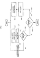
Fig. 4 illustrates a flow diagram of one method of shifting or translating
the level of an input signal in accordance with the present invention.
DETAILED DESCRIPTION OF THE INVENTION
The following description is made with reference to the appended
figures.
Many lC applications require translating one or more signals from one
voltage level to another. Figs. 1 and 2 illustrate examples of known level
shifter circuits. The level shifter illustrated in Fig. 1 and generally designated
100 comprises six transistor devices, three PMOS devices 110, 114 and 116
and three NMOS devices 112, 118 and 120.
The illustrated level shifter 100 further requires both an input signal and
its complement (VDDO and VDDC are illustrated). Moreover, this level shifter
circuit is adapted to operate with a rail-to-rail input signal (between VSSC and
VDDC for example). This circuit 100 translates a signal referenced to VDDC
to a signal referenced to VDDO. If the complement of the input signal isn't
provided, the circuit may generate such compliment using an inverter 122
(comprising devices 110 and 112 for example) that is referenced to the input
signal level VDDC. However, this may pose a problem if the VDDC supply
isn't readily available.
Fig. 2 illustrates another example of a level shifter circuit generally
designated 200 having only a single-ended input signal. In the illustrated
embodiment, the level shifter 200 comprises at least one PMOS device 210
coupled to a REF signal and at least one NMOS device 212 coupled to an
INPUT signal. It is contemplated that this known circuit draws DC current
during operation thereon (when its input is high for example).
One embodiment of the present invention overcomes the need for a
complementary input or the need for an additional power supply (i.e., VDDC
for example) if the complementary signal isn't available. This embodiment
eliminates all static current drain (not including leakage). One embodiment of
the present invention illustrated in Fig. 3 and generally designated 300,
comprises at least three transistor devices, a first transistor device coupled to
at least an input and adapted to have a negative threshold voltage, a second
transistor device coupled to at least the first transistor device and a level
shifter transistor device coupled to at least the first and second transistor
devices.
More specifically, one embodiment of the present invention comprises
four transistors coupled as illustrated in Fig. 3. In this embodiment, VDD is
the power supply, device 310 is an NMOS transistor, devices 312 and 314 are
PMOS transistors, and device 316 is a native NMOS device adapted to have
a negative threshold voltage (i.e., the threshold voltage or Vtnative < 0V) over
all operating conditions of the level shifter circuit. In one embodiment, a level
shifter transistor device 309 comprises PMOS transistor device 312 and
NMOS transistor device 310.
It is contemplated that the threshold voltage of device 316 is always
negative (i.e., less than 0V) and is conducting when a gate to source voltage
of 0V is applied. It is further contemplated that when the input to the native
device 316 is low (i.e., GND for example) the device 316 is on. Conversely,
when the input is high (i.e., > GND for example), the native device 316 is off.
In one embodiment, when the input signal or IN is low (equal to ground
or GND for example), VDD will appear at the output (i.e., OUT = VDD). When
the input signal or IN exceeds the threshold voltage of device 310 (i.e., IN
greater than the Vt of device 310), the output signal or OUT is pulled low (i.e.,
OUT = GND for example). It is contemplated that there may be an inversion
between the IN and OUT signals. In one embodiment, adding an inverter
referenced to VDD at the output may eliminate such an inversion.
When the input signal or IN is high (i.e., IN exceeds the threshold
voltage or Vt of device 310), device 310 is on and device 316 is off. This pulls
the output signal low (i.e., OUT = GND). This turns device 314 on. The gate
of device 312 is pulled to VDD through device 314 shutting device 312 off.
Shutting device 312 off eliminates all static current drain (not including
leakage) during operation of the level shifter.
Conversely, device 316 (which has a negative Vt) conducts and device
310 is off when the input signal or IN is low (i.e., equal to GND for example).
This presents a low at the gate of device 312, which pulls the output signal or
OUT to VDD. Pulling the output signal or OUT to VDD shuts off device 314,
thereby eliminating all static current drain (not including leakage current)
during operation of the level shifter. Again, it is contemplated that the
threshold voltage of device 316 is always negative and is conducting when a
gate to source voltage of 0V is applied as provided previously.
It is further contemplated that one embodiment of the present invention
may be used in any integrated circuit application that requires shifting signal
voltage levels. Such an integrated circuit may include a level shifter
comprising at least three transistor devices; the first transistor device having a
negative threshold voltage, a second transistor device coupled to at least the
first transistor device and a level shifter transistor device coupled to at least
the first and second transistor devices as provided previously.
Yet another embodiment of the present invention relates to a method of
shifting or translating the voltage level of a signal. Fig. 4 illustrates a flow
chart depicting one method, generally designated 400, of shifting or
translating the voltage level of an input signal using only one power supply.
Referring to Figs. 3 and 4, the method comprises determining if the
input signal or IN is greater than a first threshold value as illustrated by
diamond 410. When the input signal or IN is greater than the first threshold
value, device 310 is on and device 316 is off. This pulls the output signal or
OUT low (to GND for example) as illustrated by block 412. The static current
drain is also eliminated as illustrated by block 414. When OUT is pulled low,
device 314 turns on. The gate of device 312 is pulled to VDD through device
314 shutting device 312 off. Shutting device 312 off eliminates all static
current drain (not including leakage).
The method determines if the input signal or IN is less than a second
threshold value as illustrated by diamond 415. If the input signal or IN is less
than the second threshold value or low (i.e., IN is GND for example), device
316 (which has a negative Vt) conducts and device 310 is off. This presents
a low voltage at the gate of device 312, which pulls the output signal or OUT
high (to VDD for example) as illustrated by block 416.
Again the static current drain is also eliminated as illustrated by block
418. Here, pulling OUT high shuts off device 314, thereby eliminating all
static current drain (not including leakage current) during operation of the level
shifter. Fig. 4 further illustrates that, if the input signal or IN is not less than a
second threshold value (i.e., second threshold < IN < first threshold, the
output is indeterminate as illustrated by block 420.
The known level shifter circuit (an example of which is illustrated in Fig.
1) requires an additional power supply or complementary input signal to
function. Other implementations of such known circuits that do not require
complementary inputs or dual power supplies (an example of which is
illustrated in Fig. 2) have static current dissipation, which may cause a
problem in certain applications. The level shifter circuit in accordance with one
embodiment of the present invention eliminates or avoids such problems. In
particular, the level shifter in accordance with one embodiment: (1) requires
only one power supply for operation; (2) does not require complementary
inputs for level translation; (3) operates over a wide range of input voltages;
(4) does not require a rail-to-rail input; (5) does not consume static current;
and (6) requires only four transistor devices, taking up less chip space in
comparison to known level shifters (an example of which is illustrated in Fig.
1).
Many modifications and variations of the present invention are possible
in light of the above teachings. Thus, it is to be understood that, within the
scope of the appended claims, the invention may be practiced otherwise than
as described hereinabove.