EP1369990A1 - Canceling feedback resistor loading effect in a shunt-shunt feedback circuit - Google Patents
Canceling feedback resistor loading effect in a shunt-shunt feedback circuit Download PDFInfo
- Publication number
- EP1369990A1 EP1369990A1 EP03101600A EP03101600A EP1369990A1 EP 1369990 A1 EP1369990 A1 EP 1369990A1 EP 03101600 A EP03101600 A EP 03101600A EP 03101600 A EP03101600 A EP 03101600A EP 1369990 A1 EP1369990 A1 EP 1369990A1
- Authority
- EP
- European Patent Office
- Prior art keywords
- current
- amplifier
- voltage converter
- specified
- output
- Prior art date
- Legal status (The legal status is an assumption and is not a legal conclusion. Google has not performed a legal analysis and makes no representation as to the accuracy of the status listed.)
- Granted
Links
- 230000000694 effects Effects 0.000 title abstract description 4
- 238000000034 method Methods 0.000 claims 3
- 230000008878 coupling Effects 0.000 claims 1
- 238000010168 coupling process Methods 0.000 claims 1
- 238000005859 coupling reaction Methods 0.000 claims 1
- 230000000295 complement effect Effects 0.000 abstract description 6
- 230000007423 decrease Effects 0.000 description 2
- 230000004048 modification Effects 0.000 description 2
- 238000012986 modification Methods 0.000 description 2
- 238000010586 diagram Methods 0.000 description 1
Images
Classifications
-
- H—ELECTRICITY
- H03—ELECTRONIC CIRCUITRY
- H03F—AMPLIFIERS
- H03F1/00—Details of amplifiers with only discharge tubes, only semiconductor devices or only unspecified devices as amplifying elements
- H03F1/34—Negative-feedback-circuit arrangements with or without positive feedback
Definitions
- the present invention is generally related to current to voltage converters, and more specifically to shunt-shunt feedback current to voltage converters.
- Converter 10 is a typical shunt-shunt feedback current to voltage converter including an operational amplifier 12 having an inverting input, a non-inverting input, and an output ⁇ out .
- Converter 10 is also seen to be coupled to a load Z L , and having a feedback loop comprising of a feedback resistor R f .
- an input current 14 is coupled to the inverting input of the amplifier 12 and has a value i in .
- a typical amplifier 12 has a voltage gain represented as ⁇ v , an input impedance Z i , and an output impedance Z o .
- T DC R f R f + Z o a v
- the feedback resistor R f when the value of feedback resistor R f is small compared to the output impendence Z o , the feedback resistor R f 's loading effect decreases loop gain. To maintain the loop gain, the amplifier can have an output stage to achieve a small output impendence Z o . However, the inclusion of such a conventional output stage consumes considerable power.
- the present invention achieves technical advantages as a shunt-shunt feedback current to voltage converter including a compensating current provided at the output of the amplifier that mirrors the current at the input of the amplifier such that the amplifier does not provide current to the feedback loop, and hence, the amplifier will not see the feedback R f as a load.
- the current provided at the amplifier output mirrors the current at the input such that the amplifier does not provide any current to the feedback loop.
- a current steering digital-to-analog converter is utilized that has complementary outputs, these outputs comprising a current source and a current sink of equal values.
- the DAC provides an output sink current to the amplifier input and steers a DAC output source current to the amplifier output.
- the DAC provides an output source current to the amplifier input, and steers an output sink current to the amplifier output.
- the DAC provides complementary outputs to the amplifier input and output such that the amplifier never provides current to the feedback loop and thus does not see the feedback loop as a load which would otherwise reduce the feedback loop gain.
- a series of polarity control switches are utilized to responsively interface the currents between the DAC and the amplifier input and output. These switches responsively control the current-flow direction to the amplifier input and output as a function of whether the output is positive or negative with respect to common mode.
- Converter 20 is seen to include an additional compensating current 22 being provided at the output of the amplifier 12 that mirrors the current 14 provided at the input of the amplifier, i in .
- the compensating output current 22 is a sink current.
- the output current 22 is a source current, as shown.
- the present invention provides a unique scheme that reduces the loading effect of the feedback loop on the amplifier in a shunt-shunt feedback current to voltage converter without the disadvantage of prior art solutions which consume considerable power.
- FIG. 3A there is depicted at 30 a current steering digital to analog converter (DAC) having complementary outputs 32 and 34.
- One current output is represented as X, and the other current output is the compliment I-X.
- I is the full-scale current and 0 ⁇ X ⁇ I.
- the values of the current output at 32 and 34 is controlled by a digital input DIN shown at 36.
- an improved current steering DAC is shown at 40 in Figure 3B which provides two opposite and equal DAC output currents at outputs 42 and 44.
- a constant sink current I shown at 48 is put in series with a source current 50 having a current I-X.
- the added constant current sink 48 having current I can be trimmed to match precisely to the full-scale of the DAC 40.
- this DAC architecture 60 has three functional blocks, the current steering DAC 40, the polarity control switches 62, and the output buffer or converter 20.
- the current steering DAC 40 produces source current X and sink current X from outputs 42 and 44 according to a digital input DIN 46.
- the source current and sink current are selectively directed by the polarity control switches 62 into the output buffer 20 which is translated thereby into voltage ⁇ out .
- output ⁇ out can swing either positive or negative.
- switch P1 steers the DAC output sink current X to the amplifier inverting input
- switch P2 steers the DAC output source current X to the amplifier output. Since current through feedback resister R f is solely provided by the DAC 40, the amplifier 12 itself is not loaded by the feedback resistor R f .
- the loading of the DAC 40 output current source to the amplifier 12 is much less than any loading of resistor R f .
- switch M1 steers the DAC output source current X to the amplifier 12 inverting input, and switch M2 steers the DAC output sink current X to the amplifier output.
- this architecture utilizes a relatively small mirror current at the output of the amplifier which consumes very little power, thus providing a very efficient shunt-shunt feedback current to voltage converter 60.
Landscapes
- Engineering & Computer Science (AREA)
- Power Engineering (AREA)
- Amplifiers (AREA)
Abstract
Description
- The present invention is generally related to current to voltage converters, and more specifically to shunt-shunt feedback current to voltage converters.
- Current to voltage converters are utilized in a number of applications including electronic devices. One particular type of current to voltage converter is a shunt-shunt feedback current to voltage converter, such as depicted at 10 in Figure 1.
Converter 10 is a typical shunt-shunt feedback current to voltage converter including anoperational amplifier 12 having an inverting input, a non-inverting input, and an output νout.Converter 10 is also seen to be coupled to a load ZL, and having a feedback loop comprising of a feedback resistor Rf . As depicted, aninput current 14 is coupled to the inverting input of theamplifier 12 and has a value iin . - A
typical amplifier 12 has a voltage gain represented as αv , an input impedance Zi , and an output impedance Zo. The feedback loop gain can be represented by: - Thus, when the value of feedback resistor Rf is small compared to the output impendence Zo , the feedback resistor Rf 's loading effect decreases loop gain. To maintain the loop gain, the amplifier can have an output stage to achieve a small output impendence Zo . However, the inclusion of such a conventional output stage consumes considerable power.
- There is desired an improved shunt-shunt feedback current to voltage converter that reduces or eliminates the loading of the amplifier by the feedback loop resistor Rf.
- The present invention achieves technical advantages as a shunt-shunt feedback current to voltage converter including a compensating current provided at the output of the amplifier that mirrors the current at the input of the amplifier such that the amplifier does not provide current to the feedback loop, and hence, the amplifier will not see the feedback Rf as a load. Advantageously, the current provided at the amplifier output mirrors the current at the input such that the amplifier does not provide any current to the feedback loop.
- In one preferred embodiment, a current steering digital-to-analog converter (DAC) is utilized that has complementary outputs, these outputs comprising a current source and a current sink of equal values. When the output of the amplifier is positive with respect to common mode, the DAC provides an output sink current to the amplifier input and steers a DAC output source current to the amplifier output. Conversely, when the output of the amplifier is negative with respect to common mode, the DAC provides an output source current to the amplifier input, and steers an output sink current to the amplifier output. Thus, depending on whether the output of the amplifier is positive or negative, the DAC provides complementary outputs to the amplifier input and output such that the amplifier never provides current to the feedback loop and thus does not see the feedback loop as a load which would otherwise reduce the feedback loop gain.
- Preferably, a series of polarity control switches are utilized to responsively interface the currents between the DAC and the amplifier input and output. These switches responsively control the current-flow direction to the amplifier input and output as a function of whether the output is positive or negative with respect to common mode.
-
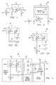
- Figure 1 is a schematic of a conventional shunt-shunt feedback current to voltage converter whereby the feedback resistor Rf tends to load the amplifier and decrease the feedback loop gain;
- Figure 2 is a schematic of the present invention including a compensating current provided at the output of the amplifier which mirrors the current at the input of the amplifier such that the amplifier provides no current to the feedback loop and thus the feedback resister Rf is not seen as a load;
- Figure 3A and Figure 3B depict a block diagram of a current steering DAC providing a complementary output and an opposite output, respectively; and
- Figure 4 is an overall DAC architecture including a current steering DAC providing a current and a complementary current of equal magnitude via a plurality of polarity control switches to a shunt-shunt feedback current to voltage converter according to the present invention.
-
- Referring now to Figure 2, there is shown generally at 20 an improved shunt-shunt feedback current to voltage converter according to a preferred embodiment of the present invention.
Converter 20 is seen to include an additional compensatingcurrent 22 being provided at the output of theamplifier 12 that mirrors the current 14 provided at the input of the amplifier, iin. Advantageously, if theinput current 14 is a source current, then thecompensating output current 22 is a sink current. Conversely, if theinput current 14 is a sink current, such as shown, then theoutput current 22 is a source current, as shown. Advantageously, by providing the additional compensatingcurrent 22 at the output of theamplifier 12 that mirrors theinput current 14, the feedback resistor Rf will not be seen as a load to theamplifier 12, and thus,amplifier 12 will not provide any current through the feedback loop, resistor Rf. Thus, the feedback loop DC gain become TDC = av. Therefore, the present invention provides a unique scheme that reduces the loading effect of the feedback loop on the amplifier in a shunt-shunt feedback current to voltage converter without the disadvantage of prior art solutions which consume considerable power. - Referring now to Figure 3A there is depicted at 30 a current steering digital to analog converter (DAC) having
complementary outputs - In the present invention two opposite and equal DAC current outputs are desired. Thus, an improved current steering DAC is shown at 40 in Figure 3B which provides two opposite and equal DAC output currents at
outputs source current 50 having a current I-X. The added constantcurrent sink 48 having current I can be trimmed to match precisely to the full-scale of theDAC 40. - Referring now to Figure 4, there is shown at 60 an overall DAC architecture according to the present invention including the
current steering DAC 40 shown in Figure 3B interfaced via a plurality of polarity control switches generally shown at 62 to the improved shunt-shunt feedback current tovoltage converter 20, as shown. Thus, thisDAC architecture 60 has three functional blocks, thecurrent steering DAC 40, the polarity control switches 62, and the output buffer orconverter 20. Thecurrent steering DAC 40 produces source current X and sink current X fromoutputs digital input DIN 46. Advantageously, the source current and sink current are selectively directed by thepolarity control switches 62 into theoutput buffer 20 which is translated thereby into voltage νout. Depending on the polarity control switch setup, output νout can swing either positive or negative. - For instance, if the νout swing needs to be positive with respect to common mode, then switches P1 and P2 of
switches 62 are closed while switches M1 and M2 are open. Thus, in this configuration switch P1 steers the DAC output sink current X to the amplifier inverting input, while switch P2 steers the DAC output source current X to the amplifier output. Since current through feedback resister Rf is solely provided by theDAC 40, theamplifier 12 itself is not loaded by the feedback resistor Rf. Advantageously, the loading of theDAC 40 output current source to theamplifier 12 is much less than any loading of resistor Rf. - Conversely, if the output νout swing needs to be negative with respect to common mode, then switch M1 steers the DAC output source current X to the
amplifier 12 inverting input, and switch M2 steers the DAC output sink current X to the amplifier output. - Advantageously, the polarity control switches 62 collectively steer the appropriate current to the input and output of the
output buffer 12 such that the current provided to the amplifier output mirrors the current provided to the amplifier input such that the feedback resistor Rf is not seen as a load to theamplifier 12, and thus, the feedback loop DC gain is TDC=av . Advantageously, this architecture utilizes a relatively small mirror current at the output of the amplifier which consumes very little power, thus providing a very efficient shunt-shunt feedback current tovoltage converter 60. - Though the invention has been described with respect to a specific preferred embodiment, many variations and modifications will become apparent to those skilled in the art upon reading the present application. It is therefore the intention that the appended claims be interpreted as broadly as possible in view of the prior art to include all such variations and modifications.
Claims (20)
- A voltage converter circuit, comprising:an amplifier having an input and an output;a feedback loop coupled between said input and said output to form a shunt-shunt current to voltage converter;an input current coupled to said input; anda compensating current mirroring said input current and being coupled to said output such that said amplifier does not provide current to said feedback loop.
- The voltage converter circuit as specified in Claim 1 wherein said input current is a sink current and said compensating current is a source current.
- The voltage converter circuit as specified in Claim 1 wherein said input current is a source current and said compensating current is a sink current.
- The voltage converter circuit as specified in any one of Claims 1 to 3 wherein said feedback loop comprises a resistor that does not load the amplifier.
- The voltage converter circuit as specified in any one of Claims 1 to 4 further comprising a capacitive load coupled to said output.
- The voltage converter circuit as specified in any one of Claims 1 to 5 wherein said amplifier has a gain of av, and said feedback loop also has a gain of av.
- The voltage converter circuit as specified in any one of Claims 1 to 6 wherein said input current and said compensating current are each provided by a current steering digital-to-analog control (DAC) circuit.
- The voltage converter circuit as specified in Claim 7 wherein said DAC provides a first current as said input current and a second current as said compensating current.
- The voltage converter circuit as specified in Claim 8 wherein said first current is a compliment of said second current such that one said current is a source current and said other current is a sink current.
- The voltage converter circuit as specified in any one of Claims 7 to 9 further comprising a switch coupling said DAC circuit to said amplifier.
- The voltage converter circuit as specified in Claim 10 wherein said switch is dynamically configurable as a function of a polarity of an output signal provided by said amplifier output.
- The voltage converter circuit as specified in Claim 11 wherein said switch is a plurality of switches configured as a polarity control switch.
- The voltage converter circuit as specified in any one of Claims 8 to 12 wherein said first current is a sink current when said amplifier output is positive, and said second current is a source current.
- The voltage converter circuit as specified in any one of Claims 8 to 12 wherein said first current is a source current when said amplifier output is negative, and said second current is a sink current.
- The voltage converter circuit as specified in any one of Claims 7 to 14 wherein the DAC input current and the compensating current load the amplifier less than a loading of the feedback loop to the amplifier.
- The voltage converter circuit as specified in any one of Claims 7 to 15 wherein the values of the input current and the compensating current are adjustably established by a digital input (DIN) control signal.
- The voltage converter circuit as specified in any one of Claims 1 to 16 wherein the amplifier is an operational amplifier.
- A method of operating a shunt-shunt current to voltage converter having an amplifier and feedback loop comprising the steps of:providing a compensating current to an output of the converter such that the amplifier does not provide current to the feedback loop.
- The method as specified in Claim 18 wherein the amplifier does not see the feedback loop as a load.
- The method as specified in Claim 18 or 19 wherein the compensating current mirrors an input current to the amplifier.
Applications Claiming Priority (2)
| Application Number | Priority Date | Filing Date | Title |
|---|---|---|---|
| US10/160,724 US6778113B2 (en) | 2002-06-03 | 2002-06-03 | Canceling feedback resister loading effect in a shunt-shunt feedback circuit |
| US160724 | 2002-06-03 |
Publications (2)
| Publication Number | Publication Date |
|---|---|
| EP1369990A1 true EP1369990A1 (en) | 2003-12-10 |
| EP1369990B1 EP1369990B1 (en) | 2009-04-01 |
Family
ID=29549280
Family Applications (1)
| Application Number | Title | Priority Date | Filing Date |
|---|---|---|---|
| EP03101600A Expired - Lifetime EP1369990B1 (en) | 2002-06-03 | 2003-06-03 | Canceling feedback resistor loading effect in a shunt-shunt feedback circuit |
Country Status (4)
| Country | Link |
|---|---|
| US (1) | US6778113B2 (en) |
| EP (1) | EP1369990B1 (en) |
| JP (1) | JP2004015806A (en) |
| DE (1) | DE60326904D1 (en) |
Families Citing this family (7)
| Publication number | Priority date | Publication date | Assignee | Title |
|---|---|---|---|---|
| US6885247B2 (en) * | 2001-12-07 | 2005-04-26 | Stmicroelectronics, Inc. | Current amplifier |
| US7154421B2 (en) * | 2003-12-12 | 2006-12-26 | Telasic Communications, Inc. | DNL/INL trim techniques for comparator based analog to digital converters |
| US9069369B1 (en) * | 2012-03-30 | 2015-06-30 | Altera Corporation | Voltage regulator and a method to operate the voltage regulator |
| US9983233B2 (en) * | 2014-02-06 | 2018-05-29 | Texas Instruments Incorporated | Current sensor |
| US9819357B1 (en) | 2017-05-11 | 2017-11-14 | Qualcomm Incorporated | Current removal for digital-to-analog converters |
| US10649477B2 (en) * | 2017-05-18 | 2020-05-12 | Cypress Semiconductor Corporation | Programmable shunt regulator |
| US10804859B2 (en) * | 2018-12-10 | 2020-10-13 | Analog Devices, Inc. | Transimpedance amplifiers with feedforward current |
Citations (5)
| Publication number | Priority date | Publication date | Assignee | Title |
|---|---|---|---|---|
| US4055812A (en) * | 1976-08-13 | 1977-10-25 | Rca Corporation | Current subtractor |
| US4642551A (en) * | 1985-10-22 | 1987-02-10 | Motorola, Inc. | Current to voltage converter circuit |
| US5625357A (en) * | 1995-02-16 | 1997-04-29 | Advanced Micro Devices, Inc. | Current steering semi-digital reconstruction filter |
| JPH09252224A (en) * | 1996-03-15 | 1997-09-22 | Rohm Co Ltd | Current / voltage conversion circuit |
| EP0911978A1 (en) * | 1997-10-23 | 1999-04-28 | STMicroelectronics S.r.l. | Generation of temperature compensation low noise symmetrical reference voltages |
Family Cites Families (5)
| Publication number | Priority date | Publication date | Assignee | Title |
|---|---|---|---|---|
| US4488144A (en) * | 1980-05-01 | 1984-12-11 | Analogic Corporation | High linearity digital to analog converter |
| KR100198541B1 (en) * | 1996-08-26 | 1999-06-15 | 구자홍 | Method for storing image frame data in memory |
| CN1143427C (en) * | 1999-09-02 | 2004-03-24 | 深圳赛意法微电子有限公司 | Mutual impedance amplifier |
| US6211661B1 (en) * | 2000-04-14 | 2001-04-03 | International Business Machines Corporation | Tunable constant current source with temperature and power supply compensation |
| US6353366B1 (en) * | 2000-04-28 | 2002-03-05 | Telecommunications Laboratories | Bandwidth enhancement of transimpedance amplifier by capacitive peaking design |
-
2002
- 2002-06-03 US US10/160,724 patent/US6778113B2/en not_active Expired - Lifetime
-
2003
- 2003-06-02 JP JP2003156676A patent/JP2004015806A/en not_active Abandoned
- 2003-06-03 DE DE60326904T patent/DE60326904D1/en not_active Expired - Lifetime
- 2003-06-03 EP EP03101600A patent/EP1369990B1/en not_active Expired - Lifetime
Patent Citations (5)
| Publication number | Priority date | Publication date | Assignee | Title |
|---|---|---|---|---|
| US4055812A (en) * | 1976-08-13 | 1977-10-25 | Rca Corporation | Current subtractor |
| US4642551A (en) * | 1985-10-22 | 1987-02-10 | Motorola, Inc. | Current to voltage converter circuit |
| US5625357A (en) * | 1995-02-16 | 1997-04-29 | Advanced Micro Devices, Inc. | Current steering semi-digital reconstruction filter |
| JPH09252224A (en) * | 1996-03-15 | 1997-09-22 | Rohm Co Ltd | Current / voltage conversion circuit |
| EP0911978A1 (en) * | 1997-10-23 | 1999-04-28 | STMicroelectronics S.r.l. | Generation of temperature compensation low noise symmetrical reference voltages |
Non-Patent Citations (1)
| Title |
|---|
| PATENT ABSTRACTS OF JAPAN vol. 1998, no. 01 30 January 1998 (1998-01-30) * |
Also Published As
| Publication number | Publication date |
|---|---|
| EP1369990B1 (en) | 2009-04-01 |
| JP2004015806A (en) | 2004-01-15 |
| US6778113B2 (en) | 2004-08-17 |
| US20030223254A1 (en) | 2003-12-04 |
| DE60326904D1 (en) | 2009-05-14 |
Similar Documents
| Publication | Publication Date | Title |
|---|---|---|
| KR102629644B1 (en) | Class-D amplifier with multiple independent output stages | |
| US5666086A (en) | Filter circuit employing a current amplifier having a fully differential output without a D.C. bias | |
| JP2000183672A (en) | Amplifier circuit | |
| ATE430404T1 (en) | DIFFERENTIAL OPERATION AMPLIFIER | |
| JPH10173445A (en) | amplifier | |
| EP0727049A1 (en) | Transconductance amplifier having a digitally variable transconductance as well as a variable gain stage and an automatic gain control circuit comprising such a variable gain stage | |
| US5565815A (en) | Current amplifier having a fully differential output without a d.c. bias and applications thereof | |
| US7187236B2 (en) | Rail-to-rail differential input amplification stage with main and surrogate differential pairs | |
| WO2017160556A1 (en) | Generation of voltage reference signals in a hybrid switched mode amplifier | |
| EP0415080B1 (en) | Device for converting unbalanced analog electric signals into fully-differential signals | |
| US6778113B2 (en) | Canceling feedback resister loading effect in a shunt-shunt feedback circuit | |
| EP0913926B1 (en) | Integrated power amplifier which allows parallel connections | |
| US6411165B1 (en) | Active common mode feedback for unbalanced input and feedback signals and methods thereof | |
| US7161419B2 (en) | Sensor device and a signal amplification device of a small detection signal provided by the sensor | |
| US5781068A (en) | Transadmittance amplifier for a motor | |
| US6492924B2 (en) | Circuits, systems, and methods for signal processors that buffer a signal dependent current | |
| US20060197592A1 (en) | Variable gain amplifier | |
| US5903189A (en) | High gain low distortion bridge amplifier with feedback | |
| WO2007105282A1 (en) | Variable gain amplifier | |
| US7643573B2 (en) | Power management in a data acquisition system | |
| JPH05283955A (en) | Audio signal amplifier | |
| KR100937437B1 (en) | Gain Amplifier with Switched-Capacitor Architecture for Minimizing Settling Time | |
| US4943784A (en) | Frequency stable digitally controlled driver circuit | |
| JP2001111419A (en) | Charge pump circuit | |
| JP2666570B2 (en) | FET bias control circuit for microwave amplification |
Legal Events
| Date | Code | Title | Description |
|---|---|---|---|
| PUAI | Public reference made under article 153(3) epc to a published international application that has entered the european phase |
Free format text: ORIGINAL CODE: 0009012 |
|
| AK | Designated contracting states |
Kind code of ref document: A1 Designated state(s): AT BE BG CH CY CZ DE DK EE ES FI FR GB GR HU IE IT LI LU MC NL PT RO SE SI SK TR |
|
| AX | Request for extension of the european patent |
Extension state: AL LT LV MK |
|
| 17P | Request for examination filed |
Effective date: 20040611 |
|
| AKX | Designation fees paid |
Designated state(s): DE FR GB |
|
| GRAP | Despatch of communication of intention to grant a patent |
Free format text: ORIGINAL CODE: EPIDOSNIGR1 |
|
| GRAS | Grant fee paid |
Free format text: ORIGINAL CODE: EPIDOSNIGR3 |
|
| GRAA | (expected) grant |
Free format text: ORIGINAL CODE: 0009210 |
|
| AK | Designated contracting states |
Kind code of ref document: B1 Designated state(s): DE FR GB |
|
| REG | Reference to a national code |
Ref country code: GB Ref legal event code: FG4D |
|
| REF | Corresponds to: |
Ref document number: 60326904 Country of ref document: DE Date of ref document: 20090514 Kind code of ref document: P |
|
| PLBE | No opposition filed within time limit |
Free format text: ORIGINAL CODE: 0009261 |
|
| STAA | Information on the status of an ep patent application or granted ep patent |
Free format text: STATUS: NO OPPOSITION FILED WITHIN TIME LIMIT |
|
| 26N | No opposition filed |
Effective date: 20100105 |
|
| REG | Reference to a national code |
Ref country code: FR Ref legal event code: PLFP Year of fee payment: 14 |
|
| REG | Reference to a national code |
Ref country code: FR Ref legal event code: PLFP Year of fee payment: 15 |
|
| REG | Reference to a national code |
Ref country code: FR Ref legal event code: PLFP Year of fee payment: 16 |
|
| PGFP | Annual fee paid to national office [announced via postgrant information from national office to epo] |
Ref country code: DE Payment date: 20180608 Year of fee payment: 16 |
|
| PGFP | Annual fee paid to national office [announced via postgrant information from national office to epo] |
Ref country code: FR Payment date: 20180516 Year of fee payment: 16 |
|
| PGFP | Annual fee paid to national office [announced via postgrant information from national office to epo] |
Ref country code: GB Payment date: 20180403 Year of fee payment: 16 |
|
| REG | Reference to a national code |
Ref country code: DE Ref legal event code: R119 Ref document number: 60326904 Country of ref document: DE |
|
| GBPC | Gb: european patent ceased through non-payment of renewal fee |
Effective date: 20190603 |
|
| PG25 | Lapsed in a contracting state [announced via postgrant information from national office to epo] |
Ref country code: DE Free format text: LAPSE BECAUSE OF NON-PAYMENT OF DUE FEES Effective date: 20200101 Ref country code: GB Free format text: LAPSE BECAUSE OF NON-PAYMENT OF DUE FEES Effective date: 20190603 |
|
| PG25 | Lapsed in a contracting state [announced via postgrant information from national office to epo] |
Ref country code: FR Free format text: LAPSE BECAUSE OF NON-PAYMENT OF DUE FEES Effective date: 20190630 |