EP1369925A2 - A phase change material electronic memory structure - Google Patents
A phase change material electronic memory structure Download PDFInfo
- Publication number
- EP1369925A2 EP1369925A2 EP03252885A EP03252885A EP1369925A2 EP 1369925 A2 EP1369925 A2 EP 1369925A2 EP 03252885 A EP03252885 A EP 03252885A EP 03252885 A EP03252885 A EP 03252885A EP 1369925 A2 EP1369925 A2 EP 1369925A2
- Authority
- EP
- European Patent Office
- Prior art keywords
- phase change
- change material
- conductor
- layer
- interconnection layer
- Prior art date
- Legal status (The legal status is an assumption and is not a legal conclusion. Google has not performed a legal analysis and makes no representation as to the accuracy of the status listed.)
- Withdrawn
Links
Images






Classifications
-
- H—ELECTRICITY
- H10—SEMICONDUCTOR DEVICES; ELECTRIC SOLID-STATE DEVICES NOT OTHERWISE PROVIDED FOR
- H10B—ELECTRONIC MEMORY DEVICES
- H10B63/00—Resistance change memory devices, e.g. resistive RAM [ReRAM] devices
- H10B63/80—Arrangements comprising multiple bistable or multi-stable switching components of the same type on a plane parallel to the substrate, e.g. cross-point arrays
-
- H—ELECTRICITY
- H10—SEMICONDUCTOR DEVICES; ELECTRIC SOLID-STATE DEVICES NOT OTHERWISE PROVIDED FOR
- H10N—ELECTRIC SOLID-STATE DEVICES NOT OTHERWISE PROVIDED FOR
- H10N70/00—Solid-state devices having no potential barriers, and specially adapted for rectifying, amplifying, oscillating or switching
- H10N70/011—Manufacture or treatment of multistable switching devices
- H10N70/061—Shaping switching materials
- H10N70/063—Shaping switching materials by etching of pre-deposited switching material layers, e.g. lithography
-
- H—ELECTRICITY
- H10—SEMICONDUCTOR DEVICES; ELECTRIC SOLID-STATE DEVICES NOT OTHERWISE PROVIDED FOR
- H10N—ELECTRIC SOLID-STATE DEVICES NOT OTHERWISE PROVIDED FOR
- H10N70/00—Solid-state devices having no potential barriers, and specially adapted for rectifying, amplifying, oscillating or switching
- H10N70/20—Multistable switching devices, e.g. memristors
- H10N70/231—Multistable switching devices, e.g. memristors based on solid-state phase change, e.g. between amorphous and crystalline phases, Ovshinsky effect
-
- H—ELECTRICITY
- H10—SEMICONDUCTOR DEVICES; ELECTRIC SOLID-STATE DEVICES NOT OTHERWISE PROVIDED FOR
- H10N—ELECTRIC SOLID-STATE DEVICES NOT OTHERWISE PROVIDED FOR
- H10N70/00—Solid-state devices having no potential barriers, and specially adapted for rectifying, amplifying, oscillating or switching
- H10N70/801—Constructional details of multistable switching devices
- H10N70/821—Device geometry
- H10N70/826—Device geometry adapted for essentially vertical current flow, e.g. sandwich or pillar type devices
-
- H—ELECTRICITY
- H10—SEMICONDUCTOR DEVICES; ELECTRIC SOLID-STATE DEVICES NOT OTHERWISE PROVIDED FOR
- H10N—ELECTRIC SOLID-STATE DEVICES NOT OTHERWISE PROVIDED FOR
- H10N70/00—Solid-state devices having no potential barriers, and specially adapted for rectifying, amplifying, oscillating or switching
- H10N70/801—Constructional details of multistable switching devices
- H10N70/841—Electrodes
- H10N70/8418—Electrodes adapted for focusing electric field or current, e.g. tip-shaped
-
- Y—GENERAL TAGGING OF NEW TECHNOLOGICAL DEVELOPMENTS; GENERAL TAGGING OF CROSS-SECTIONAL TECHNOLOGIES SPANNING OVER SEVERAL SECTIONS OF THE IPC; TECHNICAL SUBJECTS COVERED BY FORMER USPC CROSS-REFERENCE ART COLLECTIONS [XRACs] AND DIGESTS
- Y10—TECHNICAL SUBJECTS COVERED BY FORMER USPC
- Y10S—TECHNICAL SUBJECTS COVERED BY FORMER USPC CROSS-REFERENCE ART COLLECTIONS [XRACs] AND DIGESTS
- Y10S438/00—Semiconductor device manufacturing: process
- Y10S438/90—Bulk effect device making
Definitions
- RAM can be used in computer systems. Generally, RAM can perform read and write operations much faster than conventional long-term storage such as hard drives. In addition, RAM is generally more compact and generally consumes less power than hard drives.
- the RAM memory cells 110, 120, 130, 140 include functionality for setting the RAM memory cells 110, 120, 130, 140 to one of at least two logical states. Each logical state represents a bit of information. Additionally, the RAM memory cells 110, 120, 130, 140 include functionality for sensing the logical state of each of the RAM memory cells 110, 120, 130, 140.
- a particular RAM memory cell structure includes a phase change material.
- Phase change material memory cells generally include data being stored by setting the phase change material to one of two physical states of the phase change material.
- a first physical state of the phase change material can include a high electrical resistance state
- a second physical state of the phase change material can include a low electrical resistance state.
- the first physical state can represent a binary zero
- the second physical state can represent a binary one.
- Figure 3 shows a phase change material RAM memory cell in greater detail.
- a bit line 310 and a word line 320 are electrically connected to a phase change material memory cell 330.
- a voltage is applied to the bit line 310 and the word line 320 that causes a current I to flow through the phase change material memory cell 330. Heat is generated that sets the state of the phase change memory cell 330.
- phase change material memory cell structure of Figure 3 A disadvantage of the phase change material memory cell structure of Figure 3 is that the conductive bit line 310 and the conductive word line 320 each conduct significant amounts of Joule heating away from the phase change material memory cell 330, as is designated by H and the associated arrows of Figure 3. Therefore, in order for the phase change material memory cell 330 to be heated enough to set a proper physical state, a greater voltage and resulting current must be applied to compensate for the heat conducted away from the phase change memory cell 330 by the conductive bit line 310 and the conductive word line 320, than would be required without the conductive bit line 310 and the conductive word line 320 conducting heat. Generally, applying a greater amount of voltage and current is undesirable because this requires more power to be used by the RAM structure.
- the heat conduction away from the selected phase change material memory cell 330 can cause neighboring phase change material memory cells to be partially heated.
- the partial heating can cause the neighboring phase change material memory cells to start to change physical states. This effect is generally referred to as cross-talk, and should be minimized.
- phase change material memory element structure that provide more efficient heating of the phase change material within the phase change material memory element structure.
- the phase change material memory element structure should be easy to fabricate.
- the phase change material memory element structure should minimize the effects of cross-talk between neighboring phase change material memory elements within an array of phase change material memory elements.
- the invention includes a phase change material memory element structure, and method of forming, that provides more efficient heating of a phase change material within the phase change material memory element structure.
- the phase change material memory element structure is easy to fabricate.
- the phase change material memory element structure minimizes the effects of cross-talk between neighboring phase change material memory elements within an array of phase change material memory elements.
- a first embodiment of the invention includes an electronic memory structure.
- the electronic memory structure includes a substrate.
- a substantially planar first conductor is formed adjacent to the substrate.
- An interconnection layer is formed adjacent to the first conductor.
- a phase change material element is formed adjacent to the interconnection layer.
- the interconnection layer includes a conductive interconnect structure extending from the first conductor to the phase change material element.
- the interconnect structure includes a first surface physically connected to the first conductor.
- the interconnect structure further includes a second surface attached to the phase change material element. The second surface area of the second surface is substantially smaller than a first surface area of the first surface.
- a substantially planar second conductor is formed adjacent to the phase change material element.
- the phase change material layer 440 includes several phase change material layer elements 440 in which each element corresponds to a RAM cell. Not shown in Figure 4, but generally included, is an insulator material between neighboring RAM cells. That is, the insulator material (not shown) is generally located between the phase change material layer elements of neighboring RAM cells.
- the physical state of the phase change material layer 440 can be determined (read) by applying a voltage or current across the phase change material layer 440 and sensing the resulting current or voltage.
- the applied voltage or current while sensing the physical state of the phase change material layer 440 must be low enough not to change or modify the physical state of the phase change material layer 440. That is, operations to read the state of RAM phase change material layer element must not modify or alter the present physical state of the phase change material layer 440.
- the first conductive layer 420 and the second conductive layer 450 can act as heat sinks, and therefore, reduce the efficiency of modifications of the physical state of the phase change material layer 440. That is, the first conductive layer 420 and the second conductive layer 450 cause the amount of power applied to the phase change material layer 440 to change the physical state of the,phase change material layer 440 to be greater than if the first conductive layer 420 and the second conductive layer 450 did not conduct heat.
- the interconnection layer 430 provides thermal isolation between the phase change material layer 440 and the first conductive layer 420.
- a conductive interconnect structure 432 provides an electrical connection between the first conductive layer 420 and the phase change material layer 440.
- An insulator 434 is included within the conductive interconnect structures 432, and between separate conductive interconnect structures 432 associated with neighboring phase change material layer elements 440.
- phase change material layer 440 can be heated more efficiently.
- the first conductive layer 420 is not physically connected to the phase change material layer 440. Therefore, the first conductive layer 420 does not conduct nearly as much heat away from the phase change material layer 440 as it would if the first conductive layer 420 was flush with the phase change material layer 440.
- the first conductive layer 420 is formed proximate to the substrate 410.
- Proximate formation can include the first conductive layer 420 being formed directly adjacent to the substrate 410, or can include the first conductive layer 420 being separated from the substrate enough to allow for the formation of vertically oriented devices that are not directly adjacent to the substrate 410.
- Cross-talk with neighboring phase change material RAM cells is minimized because the first conductive layer 420 and the second conductive layer 450 do not conduct heat away from one phase change material layer element 440 to another phase change material layer element 440.
- the conductive interconnect structure 432 of the interconnection layer 430 can be formed by etching trenches in the interconnection layer 430.
- a conductor is formed at the edges of the trenches. The conductor forms the conductive interconnect structure 432.
- An embodiment includes the second substantially planar conductive layer 450 being physically and electrically connected to each of the phase change material layer elements 440.
- the first substantially planar conductive layer 420 can be electrically connected to each of the phase change material layer elements 440 through the conductive interconnect structure 432 of the interconnection layer 430.
- the interconnection layer 430 generally includes an insulator 434, and the conductive interconnect structure 432 that extends through the insulator 434 electrically connecting the first substantially planar conductive layer 420 to the phase change material layer elements 440.
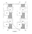
- the insulator 434 is shown in Figure 5 to show that an embodiment includes only outer comers of conductive interconnect structure 432 being physically and electrically connected to the phase change material layer elements 440.
- the embodiment of Figure 5 includes square-shaped trenches formed in the insulator 434 of the interconnection layer 430.
- the conductive interconnect structure 432 is formed over the edges of the trench. Additional insulator 434 is deposited over the conductive interconnect structure 432. The result is that only the outer edges of the square-shaped trenches are conductive, and provide an electrical connection between the first substantially conductive layer and the phase change material layer elements 440.
- the reduced contact area between the phase change material layer elements 440 and the first substantially planar conductive layer 420 addresses previously mentioned disadvantages of the prior art.
- a smaller percentage of area of the phase change material layer elements 440 is in contact with a conductor. Therefore, heat loss and thermal cross-talk are reduced.
- the reduction in heat loss enables a reduction in the amount of drive current required to crystallize the phase change material layer elements 440.
- the substrate 400 can be formed from Silicon, a Silicon Oxide, an Aluminum Oxide, a Magnesium Oxide, or other types of well-known ceramics. However, this list in not an exhaustive list. Other materials can be used to form the substrate 400.
- the conductive interconnect structure 432 of the interconnect layer 430 can be formed from Molybdenum, Tungsten, Aluminum, Titanium, Copper, Nickel or alloys thereof.
- the conductive interconnect structure 432 can also be formed from Tantalum-Silicon-Nickel. This is not an exhaustive list. Other materials can be used to form the conductive interconnect structure 432.
- the phase change material elements 440 can be formed from a group of elements selected from Te, Se, Ge, Sb, Bi, Pb, Sn, As , S. The formation of phase change materials in well-know in the field of material science.
- the second substantially planar conductive layer 450 can be formed from Copper, Aluminum, Tungsten or alloys thereof. However, this list in not an exhaustive list. Other materials can be used to form the second substantially planar conductive layer 450.
- FIG. 6 through Figure 23 show acts included within formation of an embodiment of the invention.
- Figure 6 shows a substrate 610 with a first substantially planar conductive layer 620 deposited over the substrate 610.
- the first substantially planar conductive layer 620 can be deposited by a chemical vapor deposition (CVD) process.
- the substrate can be formed from Silicon, a Silicon Oxide, an Aluminum Oxide, Glass, a Magnesium Oxide, or other types of well-known ceramics.
- the first substantially planar conductive layer 620 can be formed from Copper, Aluminum, Tungsten or alloys thereof.
- Figure 7 shows a layer of photo-resist 710 that has been deposited and patterned over the first substantially planar conductive layer 620.
- the pattern enables formation of the bit lines or word lines within the first substantially planar conductive layer 620.
- Figure 9 shows the photo-resist layer 710 having been removed leaving only the patterned first substantially planar conductive layer 810.
- the photo-resist can be removed through an etching process.
- a cross-sectional line A-A' is depicted in Figure 9 which will be used in the subsequent figures.
- Figure 11 shows the insulating dielectric layer 1010 having been polished to be substantially planar.
- a chemical mechanical polishing (CMP) process can be used to polish the insulating dielectric layer 1010.
- Figure 12 shows a lithographic patterned photo-resist 1210 having been deposited over the polished insulating dielectric layer 1010.
- the pattern determines the shape and location of the previously described trenches.
- the trenches allow formation of the previously described conductive interconnect structure 432.
- Figure 13 shows a patterned insulating dielectric layer 1310.
- the removal of the insulating dielectric providing formation of the trenches can include an oxide etch.
- the etching process can be adjusted to allow formation of sloped-edged trenches.
- the lithographic patterned photo-resist 1210 can be removed through a photo-resist ashing process.
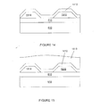
- Figure 17 shows a phase change material layer 1710 deposited over the interconnection layer 1620.
- the phase change material layer 1710 can be formed from a group of elements selected from Te, Se, Ge, Sb, Bi, Pb, Sn, As , S.
- a CVD process can be used to deposit the phase change material layer 1710.
- Figure 19 shows the phase change material layer 1710 having been etched and the photo-resist layer 1810 having been removed. Phase change material elements 1910 are left behind.
- Figure 20 shows an insulating layer 2010 having been deposited over the phase change material elements 1910, and the insulating layer 2010 having been polished.
- the insulating layer can be deposited through a CVD process and polished through a CMP process.
- Figure 21 shows the second substantially planar conductive layer 2110 having been deposited over the insulating layer 2010 and the phase change material elements 1910.
- Figure 22 shows the second substantially planar conductive layer 2110 having been patterned forming an array of conductive bit lines or word lines.
- a patterned second substantially planar conductive layer 2210 can be obtained by depositing a lithographic patterned photo-resist, etching the second substantially planar conductive layer 2110 and removing the patterned photo-resists.
- Figure 23 shows another insulting layer having been deposited and polished.
- the insulating layer can be depositing through a CVD process, and polished through a CMP process. This new insulating layer bond with the old insulating layer 2010 to form a new insulating layer 2310.
Landscapes
- Engineering & Computer Science (AREA)
- Manufacturing & Machinery (AREA)
- Semiconductor Memories (AREA)
Abstract
Description
Claims (10)
- An electronic memory structure comprising:a substrate [410];a substantially planar first conductor [420] formed proximate to the substrate [410];an interconnection layer [430] formed adjacent to the first conductor [420];a phase change material element [440] formed adjacent to the interconnection layer [430];the interconnection layer [430] comprising:a conductive interconnect structure [432] extending from the first conductor [420] to the phase change material element [440], the interconnect structure [432] having a first surface physically connected to the first conductor [420], the interconnect structure [432] having a second surface attached to the phase change material element [440], a second surface area of the second surface being substantially smaller than a first surface area of the first surface; and
a substantially planar second conductor [450] formed adjacent to the phase change material element [440]. - The electronic memory structure of claim 1, wherein the phase change material element [440] comprises a phase change surface physically connected to the interconnection layer [430] having a phase change surface area, a minority amount of the phase change surface area being physically connected to the conductive interconnect structure [432].
- The electronic memory structure of claim 1 or 2, wherein a minority amount of the second surface of the interconnect structure [432] is physically connected to the phase change surface area.
- The electronic memory structure of any preceding claim, wherein substantially all of the first surface of the interconnect structure [432] is physically connected to the first conductor [420].
- The electronic memory structure of any preceding claim, further comprising a plurality of phase change elements [440] commonly located between the interconnect layer [430] and the second conductor [450].
- The electronic memory structure of claim 5, further comprising an insulator material between the phase change elements.
- The electronic memory structure of claim 6, wherein the insulator material comprises a dielectric.
- The electronic memory structure of any preceding claim, wherein the first conductor [420] and the second conductor [450] are designated as word lines and bit lines.
- An electronic memory structure comprising:a substrate [410];a substantially planar first conductor [420] formed adjacent to the substrate[410];an interconnection layer [430] formed adjacent to the first conductor [420];a phase change material element [440] formed adjacent to the interconnection layer [430];the interconnection layer [430] comprising:a conductive interconnect structure [432] extending from the first conductor [420] to the phase change material element [440], the interconnect structure [432] having a first surface physically connected to the first conductor [420], the interconnect structure [432] having a second surface attached to the phase change material element [440];the phase change material element [440] comprising a phase change surface physically connected to the interconnection layer [430], the phase change surface having a phase change surface area, a minority amount of the phase change surface area being physically connected to the conductive interconnect structure [432]; anda substantially planar second conductor [450] formed adjacent to the phase change material element [440].
- A method of forming an electronic memory structure, the method comprising:depositing a first conductor [420] on a substrate [410];depositing an interconnection layer insulator over the first conductor and the substrate;etching a trench in the interconnection layer insulator down to the first conductor;depositing an interconnection layer conductor [420] over the trench;depositing a second interconnection layer insulator over the interconnection layer conductor;polishing the second interconnection layer insulator to expose a portion of the interconnection layer conductor;depositing a phase change material [440] over a portion of the exposed portion of the interconnection layer conductor; anddepositing a second conductor [450] over the phase change material.
Applications Claiming Priority (2)
| Application Number | Priority Date | Filing Date | Title |
|---|---|---|---|
| US10/142,494 US6605821B1 (en) | 2002-05-10 | 2002-05-10 | Phase change material electronic memory structure and method for forming |
| US142494 | 2002-05-10 |
Publications (2)
| Publication Number | Publication Date |
|---|---|
| EP1369925A2 true EP1369925A2 (en) | 2003-12-10 |
| EP1369925A3 EP1369925A3 (en) | 2005-06-15 |
Family
ID=27660882
Family Applications (1)
| Application Number | Title | Priority Date | Filing Date |
|---|---|---|---|
| EP03252885A Withdrawn EP1369925A3 (en) | 2002-05-10 | 2003-05-08 | A phase change material electronic memory structure |
Country Status (4)
| Country | Link |
|---|---|
| US (1) | US6605821B1 (en) |
| EP (1) | EP1369925A3 (en) |
| JP (1) | JP2003332530A (en) |
| CN (1) | CN1457058A (en) |
Families Citing this family (176)
| Publication number | Priority date | Publication date | Assignee | Title |
|---|---|---|---|---|
| US6649928B2 (en) * | 2000-12-13 | 2003-11-18 | Intel Corporation | Method to selectively remove one side of a conductive bottom electrode of a phase-change memory cell and structure obtained thereby |
| US6864503B2 (en) * | 2002-08-09 | 2005-03-08 | Macronix International Co., Ltd. | Spacer chalcogenide memory method and device |
| US7161167B2 (en) * | 2003-08-04 | 2007-01-09 | Intel Corporation | Lateral phase change memory |
| US20050029504A1 (en) * | 2003-08-04 | 2005-02-10 | Karpov Ilya V. | Reducing parasitic conductive paths in phase change memories |
| KR100568109B1 (en) * | 2003-11-24 | 2006-04-05 | 삼성전자주식회사 | Phase change memory device and its formation method |
| KR100558548B1 (en) * | 2003-11-27 | 2006-03-10 | 삼성전자주식회사 | Light Driver Circuit and Light Current Application Method in Phase Change Memory Devices |
| US7038231B2 (en) * | 2004-04-30 | 2006-05-02 | International Business Machines Corporation | Non-planarized, self-aligned, non-volatile phase-change memory array and method of formation |
| KR101006515B1 (en) | 2004-06-30 | 2011-01-10 | 주식회사 하이닉스반도체 | Phase change memory device and its manufacturing method |
| US7365355B2 (en) * | 2004-11-08 | 2008-04-29 | Ovonyx, Inc. | Programmable matrix array with phase-change material |
| US7608503B2 (en) | 2004-11-22 | 2009-10-27 | Macronix International Co., Ltd. | Side wall active pin memory and manufacturing method |
| US7220983B2 (en) * | 2004-12-09 | 2007-05-22 | Macronix International Co., Ltd. | Self-aligned small contact phase-change memory method and device |
| US7709334B2 (en) | 2005-12-09 | 2010-05-04 | Macronix International Co., Ltd. | Stacked non-volatile memory device and methods for fabricating the same |
| JP5474272B2 (en) * | 2005-03-15 | 2014-04-16 | ピーエスフォー ルクスコ エスエイアールエル | Memory device and manufacturing method thereof |
| EP1710850B1 (en) * | 2005-04-08 | 2010-01-06 | STMicroelectronics S.r.l. | Lateral phase change memory |
| US7427770B2 (en) | 2005-04-22 | 2008-09-23 | Micron Technology, Inc. | Memory array for increased bit density |
| US7514367B2 (en) * | 2005-06-17 | 2009-04-07 | Macronix International Co., Ltd. | Method for manufacturing a narrow structure on an integrated circuit |
| US7321130B2 (en) * | 2005-06-17 | 2008-01-22 | Macronix International Co., Ltd. | Thin film fuse phase change RAM and manufacturing method |
| US7534647B2 (en) | 2005-06-17 | 2009-05-19 | Macronix International Co., Ltd. | Damascene phase change RAM and manufacturing method |
| US7514288B2 (en) * | 2005-06-17 | 2009-04-07 | Macronix International Co., Ltd. | Manufacturing methods for thin film fuse phase change ram |
| US7598512B2 (en) * | 2005-06-17 | 2009-10-06 | Macronix International Co., Ltd. | Thin film fuse phase change cell with thermal isolation layer and manufacturing method |
| US8237140B2 (en) * | 2005-06-17 | 2012-08-07 | Macronix International Co., Ltd. | Self-aligned, embedded phase change RAM |
| US7696503B2 (en) | 2005-06-17 | 2010-04-13 | Macronix International Co., Ltd. | Multi-level memory cell having phase change element and asymmetrical thermal boundary |
| US7238994B2 (en) | 2005-06-17 | 2007-07-03 | Macronix International Co., Ltd. | Thin film plate phase change ram circuit and manufacturing method |
| KR100993664B1 (en) | 2005-10-17 | 2010-11-10 | 르네사스 일렉트로닉스 가부시키가이샤 | Semiconductor device and manufacturing method thereof |
| US7601995B2 (en) * | 2005-10-27 | 2009-10-13 | Infineon Technologies Ag | Integrated circuit having resistive memory cells |
| US7397060B2 (en) * | 2005-11-14 | 2008-07-08 | Macronix International Co., Ltd. | Pipe shaped phase change memory |
| US20070111429A1 (en) * | 2005-11-14 | 2007-05-17 | Macronix International Co., Ltd. | Method of manufacturing a pipe shaped phase change memory |
| US7635855B2 (en) | 2005-11-15 | 2009-12-22 | Macronix International Co., Ltd. | I-shaped phase change memory cell |
| US7786460B2 (en) | 2005-11-15 | 2010-08-31 | Macronix International Co., Ltd. | Phase change memory device and manufacturing method |
| US7394088B2 (en) | 2005-11-15 | 2008-07-01 | Macronix International Co., Ltd. | Thermally contained/insulated phase change memory device and method (combined) |
| US7450411B2 (en) | 2005-11-15 | 2008-11-11 | Macronix International Co., Ltd. | Phase change memory device and manufacturing method |
| US7414258B2 (en) | 2005-11-16 | 2008-08-19 | Macronix International Co., Ltd. | Spacer electrode small pin phase change memory RAM and manufacturing method |
| JP4628935B2 (en) * | 2005-11-19 | 2011-02-09 | エルピーダメモリ株式会社 | Nonvolatile semiconductor memory device |
| CN100524878C (en) | 2005-11-21 | 2009-08-05 | 旺宏电子股份有限公司 | Programmable resistive material memory array with air-insulated cells |
| US7449710B2 (en) * | 2005-11-21 | 2008-11-11 | Macronix International Co., Ltd. | Vacuum jacket for phase change memory element |
| US7507986B2 (en) | 2005-11-21 | 2009-03-24 | Macronix International Co., Ltd. | Thermal isolation for an active-sidewall phase change memory cell |
| US7829876B2 (en) | 2005-11-21 | 2010-11-09 | Macronix International Co., Ltd. | Vacuum cell thermal isolation for a phase change memory device |
| US7479649B2 (en) | 2005-11-21 | 2009-01-20 | Macronix International Co., Ltd. | Vacuum jacketed electrode for phase change memory element |
| US7599217B2 (en) | 2005-11-22 | 2009-10-06 | Macronix International Co., Ltd. | Memory cell device and manufacturing method |
| US7688619B2 (en) | 2005-11-28 | 2010-03-30 | Macronix International Co., Ltd. | Phase change memory cell and manufacturing method |
| JP4847743B2 (en) * | 2005-11-28 | 2011-12-28 | エルピーダメモリ株式会社 | Nonvolatile memory device |
| US7459717B2 (en) | 2005-11-28 | 2008-12-02 | Macronix International Co., Ltd. | Phase change memory cell and manufacturing method |
| US7521364B2 (en) | 2005-12-02 | 2009-04-21 | Macronix Internation Co., Ltd. | Surface topology improvement method for plug surface areas |
| JP4017650B2 (en) * | 2005-12-02 | 2007-12-05 | シャープ株式会社 | Variable resistance element and manufacturing method thereof |
| JP4939324B2 (en) * | 2005-12-02 | 2012-05-23 | シャープ株式会社 | Variable resistance element and manufacturing method thereof |
| JP4061328B2 (en) * | 2005-12-02 | 2008-03-19 | シャープ株式会社 | Variable resistance element and manufacturing method thereof |
| US7605079B2 (en) * | 2005-12-05 | 2009-10-20 | Macronix International Co., Ltd. | Manufacturing method for phase change RAM with electrode layer process |
| US7642539B2 (en) * | 2005-12-13 | 2010-01-05 | Macronix International Co., Ltd. | Thin film fuse phase change cell with thermal isolation pad and manufacturing method |
| US7531825B2 (en) | 2005-12-27 | 2009-05-12 | Macronix International Co., Ltd. | Method for forming self-aligned thermal isolation cell for a variable resistance memory array |
| US8062833B2 (en) * | 2005-12-30 | 2011-11-22 | Macronix International Co., Ltd. | Chalcogenide layer etching method |
| US7560337B2 (en) | 2006-01-09 | 2009-07-14 | Macronix International Co., Ltd. | Programmable resistive RAM and manufacturing method |
| US7741636B2 (en) * | 2006-01-09 | 2010-06-22 | Macronix International Co., Ltd. | Programmable resistive RAM and manufacturing method |
| US7595218B2 (en) * | 2006-01-09 | 2009-09-29 | Macronix International Co., Ltd. | Programmable resistive RAM and manufacturing method |
| US7825396B2 (en) * | 2006-01-11 | 2010-11-02 | Macronix International Co., Ltd. | Self-align planerized bottom electrode phase change memory and manufacturing method |
| US7432206B2 (en) * | 2006-01-24 | 2008-10-07 | Macronix International Co., Ltd. | Self-aligned manufacturing method, and manufacturing method for thin film fuse phase change ram |
| US7456421B2 (en) * | 2006-01-30 | 2008-11-25 | Macronix International Co., Ltd. | Vertical side wall active pin structures in a phase change memory and manufacturing methods |
| US7956358B2 (en) * | 2006-02-07 | 2011-06-07 | Macronix International Co., Ltd. | I-shaped phase change memory cell with thermal isolation |
| US7910907B2 (en) | 2006-03-15 | 2011-03-22 | Macronix International Co., Ltd. | Manufacturing method for pipe-shaped electrode phase change memory |
| US7554144B2 (en) * | 2006-04-17 | 2009-06-30 | Macronix International Co., Ltd. | Memory device and manufacturing method |
| US7928421B2 (en) | 2006-04-21 | 2011-04-19 | Macronix International Co., Ltd. | Phase change memory cell with vacuum spacer |
| US8129706B2 (en) * | 2006-05-05 | 2012-03-06 | Macronix International Co., Ltd. | Structures and methods of a bistable resistive random access memory |
| US7608848B2 (en) * | 2006-05-09 | 2009-10-27 | Macronix International Co., Ltd. | Bridge resistance random access memory device with a singular contact structure |
| US7423300B2 (en) | 2006-05-24 | 2008-09-09 | Macronix International Co., Ltd. | Single-mask phase change memory element |
| US7732800B2 (en) * | 2006-05-30 | 2010-06-08 | Macronix International Co., Ltd. | Resistor random access memory cell with L-shaped electrode |
| US7820997B2 (en) * | 2006-05-30 | 2010-10-26 | Macronix International Co., Ltd. | Resistor random access memory cell with reduced active area and reduced contact areas |
| US7696506B2 (en) | 2006-06-27 | 2010-04-13 | Macronix International Co., Ltd. | Memory cell with memory material insulation and manufacturing method |
| US7785920B2 (en) | 2006-07-12 | 2010-08-31 | Macronix International Co., Ltd. | Method for making a pillar-type phase change memory element |
| US7442603B2 (en) * | 2006-08-16 | 2008-10-28 | Macronix International Co., Ltd. | Self-aligned structure and method for confining a melting point in a resistor random access memory |
| US7560723B2 (en) * | 2006-08-29 | 2009-07-14 | Micron Technology, Inc. | Enhanced memory density resistance variable memory cells, arrays, devices and systems including the same, and methods of fabrication |
| US7772581B2 (en) | 2006-09-11 | 2010-08-10 | Macronix International Co., Ltd. | Memory device having wide area phase change element and small electrode contact area |
| US7504653B2 (en) * | 2006-10-04 | 2009-03-17 | Macronix International Co., Ltd. | Memory cell device with circumferentially-extending memory element |
| US7510929B2 (en) * | 2006-10-18 | 2009-03-31 | Macronix International Co., Ltd. | Method for making memory cell device |
| US7863655B2 (en) | 2006-10-24 | 2011-01-04 | Macronix International Co., Ltd. | Phase change memory cells with dual access devices |
| US20080094885A1 (en) * | 2006-10-24 | 2008-04-24 | Macronix International Co., Ltd. | Bistable Resistance Random Access Memory Structures with Multiple Memory Layers and Multilevel Memory States |
| US7388771B2 (en) * | 2006-10-24 | 2008-06-17 | Macronix International Co., Ltd. | Methods of operating a bistable resistance random access memory with multiple memory layers and multilevel memory states |
| US7527985B2 (en) * | 2006-10-24 | 2009-05-05 | Macronix International Co., Ltd. | Method for manufacturing a resistor random access memory with reduced active area and reduced contact areas |
| US8067762B2 (en) | 2006-11-16 | 2011-11-29 | Macronix International Co., Ltd. | Resistance random access memory structure for enhanced retention |
| US7476587B2 (en) | 2006-12-06 | 2009-01-13 | Macronix International Co., Ltd. | Method for making a self-converged memory material element for memory cell |
| US7682868B2 (en) | 2006-12-06 | 2010-03-23 | Macronix International Co., Ltd. | Method for making a keyhole opening during the manufacture of a memory cell |
| US7473576B2 (en) * | 2006-12-06 | 2009-01-06 | Macronix International Co., Ltd. | Method for making a self-converged void and bottom electrode for memory cell |
| US7697316B2 (en) * | 2006-12-07 | 2010-04-13 | Macronix International Co., Ltd. | Multi-level cell resistance random access memory with metal oxides |
| US7903447B2 (en) * | 2006-12-13 | 2011-03-08 | Macronix International Co., Ltd. | Method, apparatus and computer program product for read before programming process on programmable resistive memory cell |
| US8344347B2 (en) | 2006-12-15 | 2013-01-01 | Macronix International Co., Ltd. | Multi-layer electrode structure |
| US7718989B2 (en) * | 2006-12-28 | 2010-05-18 | Macronix International Co., Ltd. | Resistor random access memory cell device |
| US7515461B2 (en) * | 2007-01-05 | 2009-04-07 | Macronix International Co., Ltd. | Current compliant sensing architecture for multilevel phase change memory |
| US7433226B2 (en) | 2007-01-09 | 2008-10-07 | Macronix International Co., Ltd. | Method, apparatus and computer program product for read before programming process on multiple programmable resistive memory cell |
| US7440315B2 (en) | 2007-01-09 | 2008-10-21 | Macronix International Co., Ltd. | Method, apparatus and computer program product for stepped reset programming process on programmable resistive memory cell |
| US7663135B2 (en) | 2007-01-31 | 2010-02-16 | Macronix International Co., Ltd. | Memory cell having a side electrode contact |
| US7535756B2 (en) | 2007-01-31 | 2009-05-19 | Macronix International Co., Ltd. | Method to tighten set distribution for PCRAM |
| US7619311B2 (en) | 2007-02-02 | 2009-11-17 | Macronix International Co., Ltd. | Memory cell device with coplanar electrode surface and method |
| US7701759B2 (en) | 2007-02-05 | 2010-04-20 | Macronix International Co., Ltd. | Memory cell device and programming methods |
| US7483292B2 (en) * | 2007-02-07 | 2009-01-27 | Macronix International Co., Ltd. | Memory cell with separate read and program paths |
| US7463512B2 (en) | 2007-02-08 | 2008-12-09 | Macronix International Co., Ltd. | Memory element with reduced-current phase change element |
| US8138028B2 (en) | 2007-02-12 | 2012-03-20 | Macronix International Co., Ltd | Method for manufacturing a phase change memory device with pillar bottom electrode |
| US7884343B2 (en) | 2007-02-14 | 2011-02-08 | Macronix International Co., Ltd. | Phase change memory cell with filled sidewall memory element and method for fabricating the same |
| US7619237B2 (en) * | 2007-02-21 | 2009-11-17 | Macronix International Co., Ltd. | Programmable resistive memory cell with self-forming gap |
| US8008643B2 (en) * | 2007-02-21 | 2011-08-30 | Macronix International Co., Ltd. | Phase change memory cell with heater and method for fabricating the same |
| US7956344B2 (en) * | 2007-02-27 | 2011-06-07 | Macronix International Co., Ltd. | Memory cell with memory element contacting ring-shaped upper end of bottom electrode |
| US7786461B2 (en) | 2007-04-03 | 2010-08-31 | Macronix International Co., Ltd. | Memory structure with reduced-size memory element between memory material portions |
| US8610098B2 (en) | 2007-04-06 | 2013-12-17 | Macronix International Co., Ltd. | Phase change memory bridge cell with diode isolation device |
| US7755076B2 (en) | 2007-04-17 | 2010-07-13 | Macronix International Co., Ltd. | 4F2 self align side wall active phase change memory |
| US7569844B2 (en) * | 2007-04-17 | 2009-08-04 | Macronix International Co., Ltd. | Memory cell sidewall contacting side electrode |
| US7483316B2 (en) * | 2007-04-24 | 2009-01-27 | Macronix International Co., Ltd. | Method and apparatus for refreshing programmable resistive memory |
| US7888719B2 (en) * | 2007-05-23 | 2011-02-15 | Taiwan Semiconductor Manufacturing Co., Ltd. | Semiconductor memory structures |
| TWI336128B (en) * | 2007-05-31 | 2011-01-11 | Ind Tech Res Inst | Phase change memory devices and fabrication methods thereof |
| US8410607B2 (en) * | 2007-06-15 | 2013-04-02 | Taiwan Semiconductor Manufacturing Co., Ltd. | Semiconductor memory structures |
| US7663134B2 (en) * | 2007-07-10 | 2010-02-16 | Taiwan Semiconductor Manufacturing Company, Ltd. | Memory array with a selector connected to multiple resistive cells |
| US8513637B2 (en) | 2007-07-13 | 2013-08-20 | Macronix International Co., Ltd. | 4F2 self align fin bottom electrodes FET drive phase change memory |
| TWI402980B (en) | 2007-07-20 | 2013-07-21 | Macronix Int Co Ltd | Resistive memory structure with buffer layer |
| US7884342B2 (en) | 2007-07-31 | 2011-02-08 | Macronix International Co., Ltd. | Phase change memory bridge cell |
| US7729161B2 (en) * | 2007-08-02 | 2010-06-01 | Macronix International Co., Ltd. | Phase change memory with dual word lines and source lines and method of operating same |
| US9018615B2 (en) * | 2007-08-03 | 2015-04-28 | Macronix International Co., Ltd. | Resistor random access memory structure having a defined small area of electrical contact |
| TWI346372B (en) * | 2007-09-12 | 2011-08-01 | Nanya Technology Corp | Phase change memory array and fabrications thereof |
| US7642125B2 (en) | 2007-09-14 | 2010-01-05 | Macronix International Co., Ltd. | Phase change memory cell in via array with self-aligned, self-converged bottom electrode and method for manufacturing |
| US8178386B2 (en) | 2007-09-14 | 2012-05-15 | Macronix International Co., Ltd. | Phase change memory cell array with self-converged bottom electrode and method for manufacturing |
| US7551473B2 (en) | 2007-10-12 | 2009-06-23 | Macronix International Co., Ltd. | Programmable resistive memory with diode structure |
| US7919766B2 (en) | 2007-10-22 | 2011-04-05 | Macronix International Co., Ltd. | Method for making self aligning pillar memory cell device |
| US7804083B2 (en) | 2007-11-14 | 2010-09-28 | Macronix International Co., Ltd. | Phase change memory cell including a thermal protect bottom electrode and manufacturing methods |
| US7646631B2 (en) | 2007-12-07 | 2010-01-12 | Macronix International Co., Ltd. | Phase change memory cell having interface structures with essentially equal thermal impedances and manufacturing methods |
| US7639527B2 (en) | 2008-01-07 | 2009-12-29 | Macronix International Co., Ltd. | Phase change memory dynamic resistance test and manufacturing methods |
| US7879643B2 (en) | 2008-01-18 | 2011-02-01 | Macronix International Co., Ltd. | Memory cell with memory element contacting an inverted T-shaped bottom electrode |
| US8043888B2 (en) * | 2008-01-18 | 2011-10-25 | Freescale Semiconductor, Inc. | Phase change memory cell with heater and method therefor |
| US8563355B2 (en) * | 2008-01-18 | 2013-10-22 | Freescale Semiconductor, Inc. | Method of making a phase change memory cell having a silicide heater in conjunction with a FinFET |
| US7879645B2 (en) | 2008-01-28 | 2011-02-01 | Macronix International Co., Ltd. | Fill-in etching free pore device |
| US8158965B2 (en) | 2008-02-05 | 2012-04-17 | Macronix International Co., Ltd. | Heating center PCRAM structure and methods for making |
| JP5364280B2 (en) * | 2008-03-07 | 2013-12-11 | 株式会社東芝 | Nonvolatile memory device and manufacturing method thereof |
| US8084842B2 (en) | 2008-03-25 | 2011-12-27 | Macronix International Co., Ltd. | Thermally stabilized electrode structure |
| US8030634B2 (en) | 2008-03-31 | 2011-10-04 | Macronix International Co., Ltd. | Memory array with diode driver and method for fabricating the same |
| JP5305711B2 (en) * | 2008-03-31 | 2013-10-02 | 株式会社東芝 | Nonvolatile memory device and manufacturing method thereof |
| US7825398B2 (en) | 2008-04-07 | 2010-11-02 | Macronix International Co., Ltd. | Memory cell having improved mechanical stability |
| US7791057B2 (en) | 2008-04-22 | 2010-09-07 | Macronix International Co., Ltd. | Memory cell having a buried phase change region and method for fabricating the same |
| US8077505B2 (en) | 2008-05-07 | 2011-12-13 | Macronix International Co., Ltd. | Bipolar switching of phase change device |
| US7701750B2 (en) | 2008-05-08 | 2010-04-20 | Macronix International Co., Ltd. | Phase change device having two or more substantial amorphous regions in high resistance state |
| US8415651B2 (en) | 2008-06-12 | 2013-04-09 | Macronix International Co., Ltd. | Phase change memory cell having top and bottom sidewall contacts |
| US8134857B2 (en) | 2008-06-27 | 2012-03-13 | Macronix International Co., Ltd. | Methods for high speed reading operation of phase change memory and device employing same |
| US7932506B2 (en) | 2008-07-22 | 2011-04-26 | Macronix International Co., Ltd. | Fully self-aligned pore-type memory cell having diode access device |
| US7903457B2 (en) | 2008-08-19 | 2011-03-08 | Macronix International Co., Ltd. | Multiple phase change materials in an integrated circuit for system on a chip application |
| US7719913B2 (en) | 2008-09-12 | 2010-05-18 | Macronix International Co., Ltd. | Sensing circuit for PCRAM applications |
| US8324605B2 (en) | 2008-10-02 | 2012-12-04 | Macronix International Co., Ltd. | Dielectric mesh isolated phase change structure for phase change memory |
| US7897954B2 (en) | 2008-10-10 | 2011-03-01 | Macronix International Co., Ltd. | Dielectric-sandwiched pillar memory device |
| US8036014B2 (en) * | 2008-11-06 | 2011-10-11 | Macronix International Co., Ltd. | Phase change memory program method without over-reset |
| US8907316B2 (en) | 2008-11-07 | 2014-12-09 | Macronix International Co., Ltd. | Memory cell access device having a pn-junction with polycrystalline and single crystal semiconductor regions |
| US8664689B2 (en) | 2008-11-07 | 2014-03-04 | Macronix International Co., Ltd. | Memory cell access device having a pn-junction with polycrystalline plug and single-crystal semiconductor regions |
| US7869270B2 (en) | 2008-12-29 | 2011-01-11 | Macronix International Co., Ltd. | Set algorithm for phase change memory cell |
| US8089137B2 (en) | 2009-01-07 | 2012-01-03 | Macronix International Co., Ltd. | Integrated circuit memory with single crystal silicon on silicide driver and manufacturing method |
| US8107283B2 (en) | 2009-01-12 | 2012-01-31 | Macronix International Co., Ltd. | Method for setting PCRAM devices |
| US8030635B2 (en) | 2009-01-13 | 2011-10-04 | Macronix International Co., Ltd. | Polysilicon plug bipolar transistor for phase change memory |
| US8064247B2 (en) | 2009-01-14 | 2011-11-22 | Macronix International Co., Ltd. | Rewritable memory device based on segregation/re-absorption |
| US8933536B2 (en) | 2009-01-22 | 2015-01-13 | Macronix International Co., Ltd. | Polysilicon pillar bipolar transistor with self-aligned memory element |
| US8084760B2 (en) | 2009-04-20 | 2011-12-27 | Macronix International Co., Ltd. | Ring-shaped electrode and manufacturing method for same |
| US8173987B2 (en) | 2009-04-27 | 2012-05-08 | Macronix International Co., Ltd. | Integrated circuit 3D phase change memory array and manufacturing method |
| US8097871B2 (en) | 2009-04-30 | 2012-01-17 | Macronix International Co., Ltd. | Low operational current phase change memory structures |
| US7933139B2 (en) | 2009-05-15 | 2011-04-26 | Macronix International Co., Ltd. | One-transistor, one-resistor, one-capacitor phase change memory |
| US7968876B2 (en) | 2009-05-22 | 2011-06-28 | Macronix International Co., Ltd. | Phase change memory cell having vertical channel access transistor |
| US8350316B2 (en) | 2009-05-22 | 2013-01-08 | Macronix International Co., Ltd. | Phase change memory cells having vertical channel access transistor and memory plane |
| US8809829B2 (en) | 2009-06-15 | 2014-08-19 | Macronix International Co., Ltd. | Phase change memory having stabilized microstructure and manufacturing method |
| US8406033B2 (en) | 2009-06-22 | 2013-03-26 | Macronix International Co., Ltd. | Memory device and method for sensing and fixing margin cells |
| US8058095B2 (en) | 2009-06-23 | 2011-11-15 | Micron Technology, Inc. | Encapsulated phase change cell structures and methods |
| US8363463B2 (en) | 2009-06-25 | 2013-01-29 | Macronix International Co., Ltd. | Phase change memory having one or more non-constant doping profiles |
| US8238149B2 (en) | 2009-06-25 | 2012-08-07 | Macronix International Co., Ltd. | Methods and apparatus for reducing defect bits in phase change memory |
| US8110822B2 (en) | 2009-07-15 | 2012-02-07 | Macronix International Co., Ltd. | Thermal protect PCRAM structure and methods for making |
| US8198619B2 (en) | 2009-07-15 | 2012-06-12 | Macronix International Co., Ltd. | Phase change memory cell structure |
| US7894254B2 (en) | 2009-07-15 | 2011-02-22 | Macronix International Co., Ltd. | Refresh circuitry for phase change memory |
| US8064248B2 (en) | 2009-09-17 | 2011-11-22 | Macronix International Co., Ltd. | 2T2R-1T1R mix mode phase change memory array |
| US8178387B2 (en) | 2009-10-23 | 2012-05-15 | Macronix International Co., Ltd. | Methods for reducing recrystallization time for a phase change material |
| US8729521B2 (en) | 2010-05-12 | 2014-05-20 | Macronix International Co., Ltd. | Self aligned fin-type programmable memory cell |
| US8310864B2 (en) | 2010-06-15 | 2012-11-13 | Macronix International Co., Ltd. | Self-aligned bit line under word line memory array |
| US8395935B2 (en) | 2010-10-06 | 2013-03-12 | Macronix International Co., Ltd. | Cross-point self-aligned reduced cell size phase change memory |
| US8497705B2 (en) | 2010-11-09 | 2013-07-30 | Macronix International Co., Ltd. | Phase change device for interconnection of programmable logic device |
| US8467238B2 (en) | 2010-11-15 | 2013-06-18 | Macronix International Co., Ltd. | Dynamic pulse operation for phase change memory |
| US8987700B2 (en) | 2011-12-02 | 2015-03-24 | Macronix International Co., Ltd. | Thermally confined electrode for programmable resistance memory |
| TWI549229B (en) | 2014-01-24 | 2016-09-11 | 旺宏電子股份有限公司 | Multiple phase change materials in a memory device for system on a chip application |
| US9559113B2 (en) | 2014-05-01 | 2017-01-31 | Macronix International Co., Ltd. | SSL/GSL gate oxide in 3D vertical channel NAND |
| US9159412B1 (en) | 2014-07-15 | 2015-10-13 | Macronix International Co., Ltd. | Staggered write and verify for phase change memory |
| US9672906B2 (en) | 2015-06-19 | 2017-06-06 | Macronix International Co., Ltd. | Phase change memory with inter-granular switching |
| CN107017341B (en) * | 2017-03-28 | 2020-09-25 | 华中科技大学 | Asymmetric annular microelectrode phase change memory unit and device |
Family Cites Families (7)
| Publication number | Priority date | Publication date | Assignee | Title |
|---|---|---|---|---|
| US6147395A (en) * | 1996-10-02 | 2000-11-14 | Micron Technology, Inc. | Method for fabricating a small area of contact between electrodes |
| US5952671A (en) * | 1997-05-09 | 1999-09-14 | Micron Technology, Inc. | Small electrode for a chalcogenide switching device and method for fabricating same |
| US6031287A (en) * | 1997-06-18 | 2000-02-29 | Micron Technology, Inc. | Contact structure and memory element incorporating the same |
| US5933365A (en) | 1997-06-19 | 1999-08-03 | Energy Conversion Devices, Inc. | Memory element with energy control mechanism |
| US5912839A (en) | 1998-06-23 | 1999-06-15 | Energy Conversion Devices, Inc. | Universal memory element and method of programming same |
| WO2002009206A1 (en) * | 2000-07-22 | 2002-01-31 | Ovonyx, Inc. | Electrically programmable memory element |
| US6567293B1 (en) * | 2000-09-29 | 2003-05-20 | Ovonyx, Inc. | Single level metal memory cell using chalcogenide cladding |
-
2002
- 2002-05-10 US US10/142,494 patent/US6605821B1/en not_active Expired - Fee Related
-
2003
- 2003-03-10 CN CN03120148A patent/CN1457058A/en active Pending
- 2003-04-23 JP JP2003118298A patent/JP2003332530A/en not_active Ceased
- 2003-05-08 EP EP03252885A patent/EP1369925A3/en not_active Withdrawn
Also Published As
| Publication number | Publication date |
|---|---|
| CN1457058A (en) | 2003-11-19 |
| US6605821B1 (en) | 2003-08-12 |
| EP1369925A3 (en) | 2005-06-15 |
| JP2003332530A (en) | 2003-11-21 |
Similar Documents
| Publication | Publication Date | Title |
|---|---|---|
| US6605821B1 (en) | Phase change material electronic memory structure and method for forming | |
| US11563055B2 (en) | Self-aligned cross-point phase change memory-switch array | |
| CN110808332B (en) | semiconductor storage device | |
| KR100873973B1 (en) | Phase Change Memory Cell with High Read Margin with Low Power Operation | |
| US7408240B2 (en) | Memory device | |
| KR100293866B1 (en) | Memory array having a multi-state element and method for forming such array or cells thereof | |
| US7618840B2 (en) | Sublithographic contact structure, in particular for a phase change memory cell, and fabrication process thereof | |
| US7619247B2 (en) | Structure for amorphous carbon based non-volatile memory | |
| US7470922B2 (en) | Increasing adherence of dielectrics to phase change materials | |
| US7026639B2 (en) | Phase change memory element capable of low power operation and method of fabricating the same | |
| TWI384585B (en) | Variable resistance memory device having reduced bottom contact area and method of forming the same | |
| US20070267618A1 (en) | Memory device | |
| US20060228883A1 (en) | Phase change memory cell defined by a pattern shrink material process | |
| US8101938B2 (en) | Method of forming a chalcogenide memory cell having an ultrasmall cross-sectional area and a chalcogenide memory cell produced by the method | |
| TW200849561A (en) | Resistive memory cell fabrication methods and devices | |
| JP5435424B2 (en) | Programmable resistive memory device, system using the same, and method of forming the same | |
| US20070290185A1 (en) | Phase change memory cells and methods for fabricating the same | |
| US20240334712A1 (en) | Memory cell based on a phase-change material | |
| US20250374836A1 (en) | Electronic device comprising a memory circuit based on phase-change material | |
| CN119072135A (en) | Electronic devices | |
| JP2006303294A (en) | Variable-phase nonvolatile memory and its manufacturing method |
Legal Events
| Date | Code | Title | Description |
|---|---|---|---|
| PUAI | Public reference made under article 153(3) epc to a published international application that has entered the european phase |
Free format text: ORIGINAL CODE: 0009012 |
|
| AK | Designated contracting states |
Kind code of ref document: A2 Designated state(s): AT BE BG CH CY CZ DE DK EE ES FI FR GB GR HU IE IT LI LU MC NL PT RO SE SI SK TR |
|
| AX | Request for extension of the european patent |
Extension state: AL LT LV MK |
|
| PUAL | Search report despatched |
Free format text: ORIGINAL CODE: 0009013 |
|
| AK | Designated contracting states |
Kind code of ref document: A3 Designated state(s): AT BE BG CH CY CZ DE DK EE ES FI FR GB GR HU IE IT LI LU MC NL PT RO SE SI SK TR |
|
| AX | Request for extension of the european patent |
Extension state: AL LT LV MK |
|
| AKX | Designation fees paid | ||
| REG | Reference to a national code |
Ref country code: DE Ref legal event code: 8566 |
|
| STAA | Information on the status of an ep patent application or granted ep patent |
Free format text: STATUS: THE APPLICATION IS DEEMED TO BE WITHDRAWN |
|
| 18D | Application deemed to be withdrawn |
Effective date: 20051216 |
|
| RIN1 | Information on inventor provided before grant (corrected) |
Inventor name: BROCKLIN, ANDY VAN Inventor name: KOLL, ANDREW Inventor name: FRICKE, PETER Inventor name: PUNSALAN, DAVID Inventor name: ULMER, KURT Inventor name: KRAMER, KEN Inventor name: ELLENSON, JIM Inventor name: MEYER, NEAL Inventor name: LAZAROFF, DENNIS Inventor name: LEE, HEON |