EP1369776A2 - Information processor having delayed branch function - Google Patents
Information processor having delayed branch function Download PDFInfo
- Publication number
- EP1369776A2 EP1369776A2 EP03253206A EP03253206A EP1369776A2 EP 1369776 A2 EP1369776 A2 EP 1369776A2 EP 03253206 A EP03253206 A EP 03253206A EP 03253206 A EP03253206 A EP 03253206A EP 1369776 A2 EP1369776 A2 EP 1369776A2
- Authority
- EP
- European Patent Office
- Prior art keywords
- branch
- instruction
- information
- address
- delay slot
- Prior art date
- Legal status (The legal status is an assumption and is not a legal conclusion. Google has not performed a legal analysis and makes no representation as to the accuracy of the status listed.)
- Granted
Links
Images


Classifications
-
- G—PHYSICS
- G06—COMPUTING OR CALCULATING; COUNTING
- G06F—ELECTRIC DIGITAL DATA PROCESSING
- G06F9/00—Arrangements for program control, e.g. control units
- G06F9/06—Arrangements for program control, e.g. control units using stored programs, i.e. using an internal store of processing equipment to receive or retain programs
- G06F9/30—Arrangements for executing machine instructions, e.g. instruction decode
- G06F9/38—Concurrent instruction execution, e.g. pipeline or look ahead
- G06F9/3802—Instruction prefetching
- G06F9/3804—Instruction prefetching for branches, e.g. hedging, branch folding
- G06F9/3806—Instruction prefetching for branches, e.g. hedging, branch folding using address prediction, e.g. return stack, branch history buffer
-
- G—PHYSICS
- G06—COMPUTING OR CALCULATING; COUNTING
- G06F—ELECTRIC DIGITAL DATA PROCESSING
- G06F9/00—Arrangements for program control, e.g. control units
- G06F9/06—Arrangements for program control, e.g. control units using stored programs, i.e. using an internal store of processing equipment to receive or retain programs
- G06F9/30—Arrangements for executing machine instructions, e.g. instruction decode
- G06F9/38—Concurrent instruction execution, e.g. pipeline or look ahead
- G06F9/3802—Instruction prefetching
-
- G—PHYSICS
- G06—COMPUTING OR CALCULATING; COUNTING
- G06F—ELECTRIC DIGITAL DATA PROCESSING
- G06F9/00—Arrangements for program control, e.g. control units
- G06F9/06—Arrangements for program control, e.g. control units using stored programs, i.e. using an internal store of processing equipment to receive or retain programs
- G06F9/30—Arrangements for executing machine instructions, e.g. instruction decode
- G06F9/38—Concurrent instruction execution, e.g. pipeline or look ahead
- G06F9/3836—Instruction issuing, e.g. dynamic instruction scheduling or out of order instruction execution
- G06F9/3842—Speculative instruction execution
-
- G—PHYSICS
- G06—COMPUTING OR CALCULATING; COUNTING
- G06F—ELECTRIC DIGITAL DATA PROCESSING
- G06F9/00—Arrangements for program control, e.g. control units
- G06F9/06—Arrangements for program control, e.g. control units using stored programs, i.e. using an internal store of processing equipment to receive or retain programs
- G06F9/30—Arrangements for executing machine instructions, e.g. instruction decode
- G06F9/38—Concurrent instruction execution, e.g. pipeline or look ahead
- G06F9/3836—Instruction issuing, e.g. dynamic instruction scheduling or out of order instruction execution
- G06F9/3853—Instruction issuing, e.g. dynamic instruction scheduling or out of order instruction execution of compound instructions
Definitions
- the present invention relates to various kinds of information processors having a delayed branch function, and more particularly to a variable-length VLIW (Very Long Instruction Word) information processor having a delayed branch function.
- VLIW Very Long Instruction Word
- a branch prediction has been performed with a branch target buffer (BTB), and a delayed branch scheme has also been adopted in which a branch is executed after the execution of instructions (delay slot instructions) subsequent to a branch instruction.
- BTB branch target buffer
- delay slot instructions information on the number of steps SN is included in a branch instruction code.
- NOP No Operation
- variable-length VLIW processor as follows has been developed.
- a packing flag indicating a boundary between VLIWs is inserted in each instruction code of a VLIW so that VLIWs are variable in length.
- the variable-length VLIWs compressed VLIW
- their boundaries are detected using the value of packing flags.
- NOP instructions are added to VLIWs whose instruction length is shorter than the maximum length, before they are provided to an instruction pipeline.
- variable-length VLIW Even if a BTB output indicating a branch instruction is obtained by accessing the instruction cache and the BTB simultaneously using an instruction address, in the case of the variable-length VLIW, it is necessary to confirm up to which portion of a series of instructions, read from the instruction cache, belongs to one variable-length VLIW and then decode the VLIW so as to check which portion of the VLIW is the branch instruction, and further to read the information of the number of steps SN included in the branch instruction code.
- the number of steps SN can be variable in length without incorporating the information of the number of steps SN into the branch instruction code. In this case, there is no need to read the number of steps SN.
- processors other than the VLIW processor, also perform processes of reading instructions from the instruction cache and decoding the read instructions in a similar manner, such problems may occur in various kinds of processors having the delayed branch function.
- an information processor having a delayed branch function wherein, irrespective of whether or not information of the number of steps of delay slot instructions is included in a branch instruction code, it is possible to achieve an early confirmation of the number of steps of delay slot instructions and also to reduce the branch penalty by avoiding unnecessary pre-readings of instructions.
- an information processor having a delayed branch function, the processor comprising: an instruction cache; and an instruction read circuit for reading instruction codes from the instruction cache by addressing the instruction cache, wherein the instruction read circuit comprises:
- the number of steps of the delay slot instructions can be read directly from the storage, without decoding the instruction codes and confirming the number of steps of the delay slot instruction. Therefore, without performing unnecessary pre-readings of instructions under the assumption that the number of steps is the maximum value, it is possible to prevent a delay in providing instructions to the instruction pipeline, thereby reducing the branch penalty.
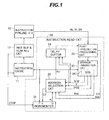
- Fig. 1 is a schematic block diagram showing a part of a processor having a delayed branch function, according to a first embodiment of the present invention.
- the processor as an information processor is a VLIW processor.
- An instruction pipeline 10 includes, for example, four parallel processing units to be able to perform spatial-parallel executions while performing temporal-parallel executions in a pipeline of each processing unit.
- Each parallel processing unit of the instruction pipeline 10 has stages of an instruction fetch, an instruction decode, an instruction execution, a memory access, and a register write.
- Fig. 5 is a schematic illustration partly showing a program stored in a main memory unit (not shown) while dividing the program into four slots in correspondence with the four-parallel instruction pipeline 10.
- the VLIW are variable in length in the program, if no NOP instruction for fixing the VLIW-length is added to the VLIW by a compiler.
- instruction codes whose head addresses are &h10C &h118 and &h124 (&h indicates a hexadecimal number), correspond to one variable-length VLIW.
- the instruction cache 11 in response to an input address Ao, the instruction cache 11 outputs 16-byte instructions whose head address is the address Ao.
- An instruction buffer & VLIW adjustment circuit 12 maintains the output instructions, and recognizes the boundary between variable-length VLIWs by detecting an instruction code whose PF is '1'.
- the circuit 12 extends a VLIW shorter than 16 bytes into a fixed-length VLIW of 16 bytes by adding NOP instructions thereto before providing it to the instruction pipeline 10. For example, referring to Fig. 5, when 16 bytes of addresses &h200 to &h20F are read and then 16 bytes of addresses &h210 to &h21F are read, 12 bytes of addresses &h208 to &h213 are recognized as a variable-length VLIW and a four-byte NOP instruction is added thereto by the instruction buffer & VLIW adjustment circuit 12. The 12 bytes of addresses &h214 to h21F are used in the same way when the next 16 bytes are read.
- An instruction read circuit 20 generates the read address for the instruction cache 11.
- the branch instruction is a delayed branch instruction, and the number of steps SN of delay slot instructions is included in the branch instruction code in this embodiment.
- a branch instruction code "JZ R1/ R2, 2" indicates that, if the content of a register R1 is 0, a branch is executed to an address corresponding to the content (R2) of a register R2, and the number of steps SN is 2.
- the delayed branch instruction is followed by VLIWs whose head addresses are &h118 &h124, and &h134 in sequence, and thus a VLIW of addresses &h118 to &h123 and a VLIW of addresses of &h124 to &h133 are the delay slot instructions.
- the delay slot instructions are executed irrespective of whether or not the branch is executed by the branch instruction.
- the procedure goes to the content (R2), for example the address &h208, of the register R2 after the delay slot instructions are executed.
- the procedure goes to the address &h134 subsequent to the delay slot instructions. Since the branch instruction and the delay slot instructions are executed temporally in parallel by the instruction pipeline 10, the branch penalty is reduced.
- All elements 21 to 25 of the instruction read circuit 20 operate in synchronism with a clock.
- the content of an incrementer 21 is composed of 28 bits obtained by omitting the lower 4 bits of 0.
- the incrementer 21 is used for outputting sequential addresses, and when a load input L is low, the content of the incrementer 21 is increased by a predetermined value of 16 in response to the rising of the clock (the value in which the lower 4 bits are omitted increases by 1).
- the load input L is high, the value on a parallel input P is loaded into the incrementer 21.
- the content of the incrementer 21 is output as an address Ai through an output Q.
- An address selection circuit 22 selects one of addresses Ai, Apb and Aab provided from the incrementer 21, a branch prediction circuit 23, and a post-prediction processing circuit 25, respectively, and then outputs it as an address Ao to the instruction cache 11, the branch prediction circuit 23, and a delay buffer 24.
- the branch prediction circuit 23 includes a branch target buffer BTB 241.
- the BTB 241 is a RAM in which a table as shown in Fig. 3 is stored. Each record of this table has the fields of a tag, a branch instruction's branch target address, a valid flag V as branch history information, and delay slot information POS regarding the number of steps of delay slot instructions.
- the valid flag V When the valid flag V is '1' or '0', it indicates that a branch was performed or not performed, respectively, by a previous branch instruction.
- the BTB 241 is addressed by an index address Ax which is lower bits of the input address Ao.
- the tag address At is compared with higher bits of the address Ao.
- the 'hit' indicates that the record has been registered in the BTB 241 and a delayed branch instruction is included in a next variable-length VLIW to be recognized by the instruction buffer & VLIW adjustment circuit 12 after being read from the instruction cache 11.
- the branch prediction circuit 23 outputs the hit signal H/M, the branch target address Apb, the valid flag V, and the delay slot information POS to provide them to the address selection circuit 22.
- Fig. 2 is a diagram showing an embodiment of the address selection circuit 22 of Fig. 1.
- the address selection circuit 22 includes two selectors 231 and 232, and a control circuit 233 which provides control signals SL1 and SL2 to selection control inputs of the two selectors 231 and 232, respectively.
- the selector 231 selects and outputs one of addresses Aab and Apb.
- the selector 232 selects one of the address Ai and the output of the selector 231, and outputs the selected one as an address Ao.
- the control circuit 233 receives the hit signal H/M, the valid flag V, the delay slot information POS, and a prediction error signal ER. Based on these signals, the control circuit 233 generates the selection control signals SL1 and SL2, and the load signal LD.
- Fig. 4 is a flow chart showing the operation of the control circuit 233 when the prediction error signal ER is low.
- the delay slot information POS is substituted for a POSX to hold the value.
- the POSX is a shift register in the control circuit 233.
- Such a loop of steps S4 to S6 allows VLIW instruction addresses of the delay slot to be sequentially read.
- the control circuit 233 causes a pulse of the load signal LD to be provided to the load input L of the incrementer 21 to load the branch target address Apb to the incrementer 21.
- the selected Ai is provided as an address Ao to the instruction cache 11, and the contents of the addresses &h120 to &h12F are read from the instruction cache 11.
- step S6 the shift register POSX is shifted to right by one bit to be '001'.
- step S6 the shift register POSX is shifted to right by one bit to be '000'.
- There is only one instruction code having PF '1' in the contents of the addresses &h200 to &h20F.
- step S1 when the procedure goes from step S1 to step S2 next time, the contents of addresses &h210 to &h21F are read from the instruction cache 11, and the VLIW of addresses &h208 to &h213 is recognized by the instruction buffer & VLIW adjustment circuit 12.
- the information POS of the number of steps SN of delay slot instructions can be read directly from the BTB 241, without decoding the instruction codes and confirming the number of steps SN. Therefore, without performing unnecessary pre-readings of instructions under the assumption that the number of steps SN is the maximum value, it is possible to prevent a delay in providing instructions to the instruction pipeline 10, thereby reducing the branch penalty.
- the address Ao, the hit signal H/M, and the valid flag V are maintained in the delay buffer 24 of FIFO.
- the decode stage of the instruction pipeline 10 indicates a branch instruction
- its branch target address Ab and the number of instruction steps SN are provided to the post-prediction processing circuit 25.
- the post-prediction processing circuit 25 reads the hit signal H/M, the valid flag V, and the address Ao corresponding to the branch instruction from the delay buffer 24.
- the valid flag V is effective only when the hit signal H/M is high.
- these SN, Ao, H/M, and V in the post-prediction processing circuit 25 are represented by [SN], [Ao], [H/M], and [V], respectively.
- the post-prediction processing circuit 25 When the hit signal H/M is low, because the record regarding this branch instruction is not present in the branch target buffer 241, the post-prediction processing circuit 25 writes it into the branch target buffer 241. In this case, the value of the flag Vr is written as the value of the valid flag V of the branch target buffer 241. In parallel with this operation, the post-prediction circuit 25 sets the prediction error signal ER high, and provides the branch target address Ab as an address Aab to the selector 231.
- the post-prediction processing circuit 25 of Fig. 1 obtains an address &h134 ⁇ &h130 next to the delay slot, and the address selection circuit 22 selects the obtained address as the address Aab and outputs the selected address as the address Ao.
- This address Ao &h130 is loaded into the incrementer 21. Accordingly, the address Ao varies as &h130, &h140 ⁇ ⁇ ⁇ , in sequence.
- Fig. 6 is a schematic illustration partly showing a program processed by the second embodiment while dividing the program into four slots in correspondence with the four-parallel instruction pipeline 10 of Fig. 1.
- a branch instruction "JZ R1, R2" having a head address &h114 is different from the branch instruction of Fig. 5 only in that the number of steps SN is not included in the branch instruction of Fig. 6. Instead of using the number of steps SN, the packing flag PF is used to designate the final step of the delay slot instructions.
- delay slot instructions range from an instruction code subsequent to a VLIW of addresses &h10 to &h117 which includes the branch instruction to an instruction code in which the PF firstly becomes 1. Namely, the delay slot instructions range from address &h118 to address &h133.
- step S5 When the prediction error signal ER is low, the operation of the control circuit 233 of Fig. 2 is the same as shown in the flow chart of Fig. 4.
- step S5 When the contents of the addresses &h130 to &h13F (corresponding to the "2" times) are read in step S5, it is determined by the instruction buffer & VLIW adjustment circuit 12 that the instruction code whose PF is '1' is the last step of the delay slot instructions.
- each VLIW among the delay slot instructions, other than the final step is at an address whose lower bits is equal to "&hF".
- the instruction buffer & VLIW adjustment circuit 12 recognizes each of the following three instruction blocks as a VLIW:
- information of the number of steps SN of delay slot instructions is not included in the branch instruction, simplifying the instruction code, and thus the configuration of the instruction pipeline 10 is simpler than that of the first embodiment.
- the processor with the delayed branch function is a variable-length VLIW processor
- the present invention since the present invention has the feature that the delay slot information POS is stored in the BTB to use it, the present invention can be also applied to fixed-length VLIW processors or various kinds of non-VLIW processors having a delayed branch function.
- branch prediction circuit 23 may also be configured such that branch history information (corresponding to the valid flag V in above embodiments) in the BTB is composed of a plurality of bits, and the branch prediction is performed by recognizing the alternating pattern of the presence and absence of branches, or based on statistical results of the presence and absence of past branches.
- branch history information corresponding to the valid flag V in above embodiments
Landscapes
- Engineering & Computer Science (AREA)
- Software Systems (AREA)
- Theoretical Computer Science (AREA)
- Physics & Mathematics (AREA)
- General Engineering & Computer Science (AREA)
- General Physics & Mathematics (AREA)
- Advance Control (AREA)
- Executing Machine-Instructions (AREA)
- Memory System Of A Hierarchy Structure (AREA)
Abstract
Description
In this case, there is no need to read the number of steps SN.
Claims (11)
- An information processor having a delayed branch function, the processor comprising: an instruction cache; and an instruction read circuit for reading instruction codes from the instruction cache by addressing the instruction cache, wherein the instruction read circuit comprises:a branch prediction circuit, including a storage in which a branch target address, branch history information, and delay slot information on a last position of delay slot instructions are stored in correspondence with an address of a branch instruction, outputting hit information as to whether or not an input address is coincident with the branch instruction address, when the coincidence is true, further outputting the delay slot information and prediction information on a presence of a branch based on the branch history information, and when the prediction information indicates that there is a branch, further outputting the branch target address;an incrementer for outputting a sequential address; andan address selection circuit for selectively outputting the branch target address or an output of the incrementer, based on the hit information, the delay slot information, and the prediction information.
- The information processor according to claim 1, wherein the address selection circuit comprises:a selector for selectively outputting the output of the incrementer or the branch target address to the branch prediction circuit; anda selection control circuit for, in synchronism with a clock, causing the selector to select the output of the incrementer when the hit information indicates that the two addresses are not identical, causing the selector to select the output of the incrementer a predetermined number of times based on the delay slot information when the hit information indicates that the coincidence is true, and further, causing the selector to select the branch target address and causing the incrementer to load the branch target address when the prediction information indicates that there is a branch.
- The information processor according to claim 1 or 2, further comprising a post-prediction processing circuit for, when the hit information indicates that the two addresses are not identical and an instruction of an address corresponding to the hit information is decoded to be a branch instruction, storing a branch target address of the branch instruction and the branch slot information in correspondence with the address of the branch instruction, and updating the corresponding branch history information of the branch target buffer on the basis of a result of judging a branch condition of the branch instruction.
- The information processor according to claim 3, wherein, when the hit information indicates that the coincidence is true, and the prediction information is different from the branch-condition judgment result, the post-prediction processing circuit makes an error signal active, and outputs an address to be executed next time on the basis of the branch-condition judgment result.
- The information processor according to claim 4, wherein, when the error signal is inactive, the address selection circuit selectively outputs the output of the incrementer or the branch target address based on the hit information, the delay slot information, and the prediction information, and
when the error signal is active, the address selection circuit outputs an address to be executed next time output from the post-prediction processing circuit occurs. - The information processor according to any of claims 3 to 5, further comprising a delay buffer for delaying the output of the selector, the hit information, and the branch history information to the post-prediction processing circuit.
- The information processor according to any preceding claim, further comprising:an instruction pipeline for receiving VLIWs; andan instruction buffer & VLIW adjustment circuit for determining a boundary between VLIWs based on a value of a packing flag in each of instruction codes included in a plurality of instructions read from the instruction cache, and adding dummy information to a VLIW so that the VLIW's instruction length is maximized if the VLIW's instruction length is less than a maximum value, and then providing the VLIW to the instruction pipeline.
- The information processor according to claim 7, wherein a delayed branch instruction of a variable-length delay slot is included in an instruction set, and information of the number of instruction steps of the variable-length delay slot is included in the delayed branch instruction, and
the instruction buffer & VLIW adjustment circuit determines instructions of the number of steps subsequent to the delayed branch instruction as a delay slot, and provides the instructions determined as the delay slot to the instruction pipeline irrespective of whether or not a branch condition of the branch instruction is satisfied. - The information processor according to claim 8, wherein the instruction buffer & VLIW adjustment circuit determines, as a delay slot, instruction codes in a range from an instruction code next to a branch instruction to an instruction code in which a packing flag firstly designates the boundary, and provides the VLIWs of the delay slot to the instruction pipeline irrespective of whether or not the branch condition of the branch instruction is satisfied.
- The information processor according to claim 9, wherein the instruction buffer & VLIW adjustment circuit determines an end of instructions read from the instruction cache at once as a boundary of a VLIW included in the delay slot.
- A method for reading instruction codes from an instruction cache of a processor, comprising the steps of:storing, in a branch prediction circuit, a branch target address, branch history information and delay slot information on a last position of delay slot instructions, in correspondence with an address of a branch instruction;outputting hit information as to whether or not an input address is coincident with the branch instruction address, when the coincidence is true, further outputting the delay slot information and prediction information on a presence of a branch based on the branch history information, and when the prediction information indicates that there is a branch, further outputting the branch target address;incrementing and outputting a sequential address; andselectively outputting the branch target address or the sequential address, based on the hit information, the delay slot information, and the prediction information.
Applications Claiming Priority (2)
| Application Number | Priority Date | Filing Date | Title |
|---|---|---|---|
| JP2002162445A JP3738842B2 (en) | 2002-06-04 | 2002-06-04 | Information processing apparatus with delayed branch function |
| JP2002162445 | 2002-06-04 |
Publications (3)
| Publication Number | Publication Date |
|---|---|
| EP1369776A2 true EP1369776A2 (en) | 2003-12-10 |
| EP1369776A3 EP1369776A3 (en) | 2006-05-31 |
| EP1369776B1 EP1369776B1 (en) | 2008-08-13 |
Family
ID=29545680
Family Applications (1)
| Application Number | Title | Priority Date | Filing Date |
|---|---|---|---|
| EP03253206A Expired - Lifetime EP1369776B1 (en) | 2002-06-04 | 2003-05-22 | Information processor having delayed branch function |
Country Status (4)
| Country | Link |
|---|---|
| US (1) | US7546445B2 (en) |
| EP (1) | EP1369776B1 (en) |
| JP (1) | JP3738842B2 (en) |
| DE (1) | DE60322785D1 (en) |
Cited By (1)
| Publication number | Priority date | Publication date | Assignee | Title |
|---|---|---|---|---|
| WO2008072178A1 (en) * | 2006-12-11 | 2008-06-19 | Nxp B.V. | Pipelined processor and compiler/scheduler for variable number branch delay slots |
Families Citing this family (11)
| Publication number | Priority date | Publication date | Assignee | Title |
|---|---|---|---|---|
| EP1378824A1 (en) * | 2002-07-02 | 2004-01-07 | STMicroelectronics S.r.l. | A method for executing programs on multiple processors and corresponding processor system |
| US7827392B2 (en) * | 2006-06-05 | 2010-11-02 | Qualcomm Incorporated | Sliding-window, block-based branch target address cache |
| JP2008071061A (en) * | 2006-09-13 | 2008-03-27 | Fujitsu Ltd | Information processing device |
| US8495341B2 (en) * | 2010-02-17 | 2013-07-23 | International Business Machines Corporation | Instruction length based cracking for instruction of variable length storage operands |
| US9703559B2 (en) | 2011-11-09 | 2017-07-11 | Nec Corporation | Digital signal processor, program control method, and control program |
| US20140180848A1 (en) * | 2012-12-20 | 2014-06-26 | Wal-Mart Stores, Inc. | Estimating Point Of Sale Wait Times |
| US10001993B2 (en) | 2013-08-08 | 2018-06-19 | Linear Algebra Technologies Limited | Variable-length instruction buffer management |
| US11768689B2 (en) | 2013-08-08 | 2023-09-26 | Movidius Limited | Apparatus, systems, and methods for low power computational imaging |
| US9535701B2 (en) * | 2014-01-29 | 2017-01-03 | Telefonaktiebolaget Lm Ericsson (Publ) | Efficient use of branch delay slots and branch prediction in pipelined computer architectures |
| US9430245B2 (en) | 2014-03-28 | 2016-08-30 | Telefonaktiebolaget Lm Ericsson (Publ) | Efficient branch predictor history recovery in pipelined computer architectures employing branch prediction and branch delay slots of variable size |
| EP4116819A1 (en) * | 2014-07-30 | 2023-01-11 | Movidius Limited | Vector processor |
Family Cites Families (7)
| Publication number | Priority date | Publication date | Assignee | Title |
|---|---|---|---|---|
| US5367703A (en) * | 1993-01-08 | 1994-11-22 | International Business Machines Corporation | Method and system for enhanced branch history prediction accuracy in a superscalar processor system |
| US5706459A (en) | 1994-01-06 | 1998-01-06 | Fujitsu Limited | Processor having a variable number of stages in a pipeline |
| US5774737A (en) * | 1995-10-13 | 1998-06-30 | Matsushita Electric Industrial Co., Ltd. | Variable word length very long instruction word instruction processor with word length register or instruction number register |
| JP3439033B2 (en) * | 1996-07-08 | 2003-08-25 | 株式会社日立製作所 | Interrupt control device and processor |
| EP1050811A1 (en) * | 1999-05-03 | 2000-11-08 | STMicroelectronics SA | Branching in a computer system |
| US6275929B1 (en) * | 1999-05-26 | 2001-08-14 | Infineon Technologies Ag L. Gr. | Delay-slot control mechanism for microprocessors |
| US6415376B1 (en) * | 2000-06-16 | 2002-07-02 | Conexant Sytems, Inc. | Apparatus and method for issue grouping of instructions in a VLIW processor |
-
2002
- 2002-06-04 JP JP2002162445A patent/JP3738842B2/en not_active Expired - Fee Related
-
2003
- 2003-05-16 US US10/438,986 patent/US7546445B2/en not_active Expired - Fee Related
- 2003-05-22 DE DE60322785T patent/DE60322785D1/en not_active Expired - Lifetime
- 2003-05-22 EP EP03253206A patent/EP1369776B1/en not_active Expired - Lifetime
Cited By (2)
| Publication number | Priority date | Publication date | Assignee | Title |
|---|---|---|---|---|
| WO2008072178A1 (en) * | 2006-12-11 | 2008-06-19 | Nxp B.V. | Pipelined processor and compiler/scheduler for variable number branch delay slots |
| US8959500B2 (en) | 2006-12-11 | 2015-02-17 | Nytell Software LLC | Pipelined processor and compiler/scheduler for variable number branch delay slots |
Also Published As
| Publication number | Publication date |
|---|---|
| JP3738842B2 (en) | 2006-01-25 |
| US20030226003A1 (en) | 2003-12-04 |
| JP2004013255A (en) | 2004-01-15 |
| EP1369776B1 (en) | 2008-08-13 |
| US7546445B2 (en) | 2009-06-09 |
| EP1369776A3 (en) | 2006-05-31 |
| DE60322785D1 (en) | 2008-09-25 |
Similar Documents
| Publication | Publication Date | Title |
|---|---|---|
| US4827402A (en) | Branch advanced control apparatus for advanced control of a branch instruction in a data processing system | |
| EP1157329B1 (en) | Methods and apparatus for branch prediction using hybrid history with index sharing | |
| US5202967A (en) | Data processing apparatus for performing parallel decoding and parallel execution of a variable word length instruction | |
| US7836287B2 (en) | Reducing the fetch time of target instructions of a predicted taken branch instruction | |
| US5193205A (en) | Pipeline processor, with return address stack storing only pre-return processed address for judging validity and correction of unprocessed address | |
| US5706459A (en) | Processor having a variable number of stages in a pipeline | |
| JP2744890B2 (en) | Branch prediction data processing apparatus and operation method | |
| US6151672A (en) | Methods and apparatus for reducing interference in a branch history table of a microprocessor | |
| US7546445B2 (en) | Information processor having delayed branch function with storing delay slot information together with branch history information | |
| JP3242508B2 (en) | Microcomputer | |
| US6631459B1 (en) | Extended instruction word folding apparatus | |
| EP0094535A2 (en) | Pipe-line data processing system | |
| EP0354740B1 (en) | Data processing apparatus for performing parallel decoding and parallel execution of a variable word length instruction | |
| US5295248A (en) | Branch control circuit | |
| US6754813B1 (en) | Apparatus and method of processing information for suppression of branch prediction | |
| US7765387B2 (en) | Program counter control method and processor thereof for controlling simultaneous execution of a plurality of instructions including branch instructions using a branch prediction mechanism and a delay instruction for branching | |
| US6016541A (en) | Instruction controlling system and method thereof | |
| US20060095746A1 (en) | Branch predictor, processor and branch prediction method | |
| US6275924B1 (en) | System for buffering instructions in a processor by reissuing instruction fetches during decoder stall time | |
| US6862680B2 (en) | Microprocessor processing specified instructions as operands | |
| US6182211B1 (en) | Conditional branch control method | |
| US20090070569A1 (en) | Branch prediction device,branch prediction method, and microprocessor | |
| US6266764B1 (en) | Program controller for switching between first program and second program | |
| US6360310B1 (en) | Apparatus and method for instruction cache access | |
| US20040019772A1 (en) | Microprocessor |
Legal Events
| Date | Code | Title | Description |
|---|---|---|---|
| PUAI | Public reference made under article 153(3) epc to a published international application that has entered the european phase |
Free format text: ORIGINAL CODE: 0009012 |
|
| AK | Designated contracting states |
Kind code of ref document: A2 Designated state(s): AT BE BG CH CY CZ DE DK EE ES FI FR GB GR HU IE IT LI LU MC NL PT RO SE SI SK TR |
|
| AX | Request for extension of the european patent |
Extension state: AL LT LV MK |
|
| PUAL | Search report despatched |
Free format text: ORIGINAL CODE: 0009013 |
|
| AK | Designated contracting states |
Kind code of ref document: A3 Designated state(s): AT BE BG CH CY CZ DE DK EE ES FI FR GB GR HU IE IT LI LU MC NL PT RO SE SI SK TR |
|
| AX | Request for extension of the european patent |
Extension state: AL LT LV MK |
|
| 17P | Request for examination filed |
Effective date: 20060809 |
|
| AKX | Designation fees paid |
Designated state(s): DE FR GB |
|
| 17Q | First examination report despatched |
Effective date: 20070402 |
|
| GRAP | Despatch of communication of intention to grant a patent |
Free format text: ORIGINAL CODE: EPIDOSNIGR1 |
|
| GRAS | Grant fee paid |
Free format text: ORIGINAL CODE: EPIDOSNIGR3 |
|
| GRAA | (expected) grant |
Free format text: ORIGINAL CODE: 0009210 |
|
| AK | Designated contracting states |
Kind code of ref document: B1 Designated state(s): DE FR GB |
|
| REG | Reference to a national code |
Ref country code: GB Ref legal event code: FG4D |
|
| REF | Corresponds to: |
Ref document number: 60322785 Country of ref document: DE Date of ref document: 20080925 Kind code of ref document: P |
|
| PLBE | No opposition filed within time limit |
Free format text: ORIGINAL CODE: 0009261 |
|
| STAA | Information on the status of an ep patent application or granted ep patent |
Free format text: STATUS: NO OPPOSITION FILED WITHIN TIME LIMIT |
|
| 26N | No opposition filed |
Effective date: 20090514 |
|
| PGFP | Annual fee paid to national office [announced via postgrant information from national office to epo] |
Ref country code: GB Payment date: 20140521 Year of fee payment: 12 |
|
| PGFP | Annual fee paid to national office [announced via postgrant information from national office to epo] |
Ref country code: DE Payment date: 20140515 Year of fee payment: 12 Ref country code: FR Payment date: 20140509 Year of fee payment: 12 |
|
| REG | Reference to a national code |
Ref country code: DE Ref legal event code: R119 Ref document number: 60322785 Country of ref document: DE |
|
| GBPC | Gb: european patent ceased through non-payment of renewal fee |
Effective date: 20150522 |
|
| REG | Reference to a national code |
Ref country code: FR Ref legal event code: ST Effective date: 20160129 |
|
| PG25 | Lapsed in a contracting state [announced via postgrant information from national office to epo] |
Ref country code: DE Free format text: LAPSE BECAUSE OF NON-PAYMENT OF DUE FEES Effective date: 20151201 Ref country code: GB Free format text: LAPSE BECAUSE OF NON-PAYMENT OF DUE FEES Effective date: 20150522 |
|
| PG25 | Lapsed in a contracting state [announced via postgrant information from national office to epo] |
Ref country code: FR Free format text: LAPSE BECAUSE OF NON-PAYMENT OF DUE FEES Effective date: 20150601 |