EP1369716A2 - Tapered optical waveguide device in semiconductor - Google Patents
Tapered optical waveguide device in semiconductor Download PDFInfo
- Publication number
- EP1369716A2 EP1369716A2 EP03011073A EP03011073A EP1369716A2 EP 1369716 A2 EP1369716 A2 EP 1369716A2 EP 03011073 A EP03011073 A EP 03011073A EP 03011073 A EP03011073 A EP 03011073A EP 1369716 A2 EP1369716 A2 EP 1369716A2
- Authority
- EP
- European Patent Office
- Prior art keywords
- taper
- waveguide
- angle
- tapered
- along
- Prior art date
- Legal status (The legal status is an assumption and is not a legal conclusion. Google has not performed a legal analysis and makes no representation as to the accuracy of the status listed.)
- Withdrawn
Links
- 230000003287 optical effect Effects 0.000 title claims abstract description 26
- 239000004065 semiconductor Substances 0.000 title claims abstract description 22
- 238000000926 separation method Methods 0.000 claims abstract description 22
- 238000000034 method Methods 0.000 claims description 24
- 230000008569 process Effects 0.000 claims description 24
- 229910052710 silicon Inorganic materials 0.000 claims description 7
- 239000010703 silicon Substances 0.000 claims description 7
- XUIMIQQOPSSXEZ-UHFFFAOYSA-N Silicon Chemical compound [Si] XUIMIQQOPSSXEZ-UHFFFAOYSA-N 0.000 description 6
- 230000005540 biological transmission Effects 0.000 description 6
- 230000008878 coupling Effects 0.000 description 5
- 238000010168 coupling process Methods 0.000 description 5
- 238000005859 coupling reaction Methods 0.000 description 5
- 238000004519 manufacturing process Methods 0.000 description 5
- 238000005530 etching Methods 0.000 description 3
- 230000007704 transition Effects 0.000 description 3
- VYPSYNLAJGMNEJ-UHFFFAOYSA-N Silicium dioxide Chemical compound O=[Si]=O VYPSYNLAJGMNEJ-UHFFFAOYSA-N 0.000 description 2
- 238000005516 engineering process Methods 0.000 description 2
- 230000004048 modification Effects 0.000 description 2
- 238000012986 modification Methods 0.000 description 2
- 239000013307 optical fiber Substances 0.000 description 2
- 238000004458 analytical method Methods 0.000 description 1
- 239000000835 fiber Substances 0.000 description 1
- 239000012212 insulator Substances 0.000 description 1
- 239000000463 material Substances 0.000 description 1
- 238000000206 photolithography Methods 0.000 description 1
- 230000005855 radiation Effects 0.000 description 1
- 239000000377 silicon dioxide Substances 0.000 description 1
- 238000004088 simulation Methods 0.000 description 1
- 239000000758 substrate Substances 0.000 description 1
Images

Classifications
-
- G—PHYSICS
- G02—OPTICS
- G02B—OPTICAL ELEMENTS, SYSTEMS OR APPARATUS
- G02B6/00—Light guides; Structural details of arrangements comprising light guides and other optical elements, e.g. couplings
- G02B6/10—Light guides; Structural details of arrangements comprising light guides and other optical elements, e.g. couplings of the optical waveguide type
- G02B6/12—Light guides; Structural details of arrangements comprising light guides and other optical elements, e.g. couplings of the optical waveguide type of the integrated circuit kind
- G02B6/122—Basic optical elements, e.g. light-guiding paths
- G02B6/1228—Tapered waveguides, e.g. integrated spot-size transformers
Definitions
- the present invention relates to semiconductor waveguides, and in particular relates to tapered waveguides, for example which are used to interconnect relatively wide waveguides with relatively narrow waveguides, and in particular to interconnect an optical fibre with a single mode semiconductor waveguide.
- the invention is described primarily in relation to rib waveguides (for example fabricated by photolithography and etching processes), but it is applicable to semiconductor waveguides generally.
- Figure 1 shows, schematically, a plan view of a Bookham Technology tapered silicon rib waveguide (not to scale), and cross sectional views of the start and end of the taper. Some typical dimensions for the taper are shown in microns.
- the width of the waveguide shown in Figure 1 reduces gradually along its length.
- the taper functions by gradually pushing the fundamental optical mode which initially substantially fills the rib section bcde down into the slab guide regions be on either side, which then form a new rib guide be at the end of the taper.
- a perfectly fabricated waveguide of this design operates with low loss. In practice, imperfections in waveguide processing can result in the taper angle exceeding the adiabatic limit (i.e.
- Figure 2 shows, schematically, a cross-section through a rib waveguide in which there are notches 1, which are imperfections resulting from the etching fabrication process.
- the size of such notches can vary up to about 0.5x0.5 microns in size.
- imperfections can result in the taper angle exceeding the adiabatic limit.
- the most straightforward way to overcome this problem would be to reduce the taper angle until the adiabatic limit is restored. However, this can result in inconveniently long tapers.
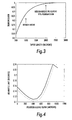
- This is illustrated by the graph of Figure 3 which shows optical transmission as a function of taper length through the taper section BC of Figure 1 for the situation where notches of 0.5 ⁇ 0.5 microns have been formed in the waveguide as shown in Figure 2.
- the design intent is typically a taper length of 1000 microns, for which optical transmission of about 97% is achievable. With the notches it is found that the transmission is reduced to about 85% and that to achieve a transmission of 97% the length of the taper section would have to be increased from 1000 to about 2000 microns, making the component impractically long.
- the graph (solid line) illustrated in Figure 4 shows a typical plot of the adiabatic limit for section BC of the taper in Figure 1 with a waveguide notch of 0.5 ⁇ 0.5 microns.
- a taper that generally follows a curve set at a fixed angle below (i.e. a constant angular separation below) the adiabatic limit, such as the dotted curve shown in Figure 4, will result in a minimum length taper for a given loss.
- a transmission of 98% is achievable in a taper following a curve 0.05 degrees below the adiabatic limit with a length of only 1206 microns, compared to a length of over 2000 microns that would be needed in a straight taper.
- the dotted curve of Figure 4 is an arbitrary constant angular separation below the adiabatic limit and is intended merely to illustrate this principle; the actual constant angular separation shown in Figure 4 is not intended to have any special relevance.
- a first aspect of the invention provides a device comprising a tapered semiconductor optical waveguide which tapers, at an angle of taper with respect to a longitudinal axis of the waveguide, from a relatively wide region to a relatively narrow region, wherein the angle of taper varies along the length of the tapered waveguide such that at all points along the taper it is no greater than, and within a substantially constant angular separation of, the adiabatic limit of the fundamental mode of the waveguide at that point along the taper.
- the relatively wide region of the tapered waveguide is a multimode region; preferably the relatively narrow region of the tapered waveguide is a single mode region.
- the transition from the relatively wide region to the relatively narrow region of the waveguide may alternatively be multimode to multimode, or single mode to single mode.
- maintaining the taper at no greater than the adiabatic limit suppresses coupling to radiation modes.
- the angle of taper at any particular point along the tapered waveguide is the angle that a lateral surface (or, for curved waveguides, the tangent of the lateral surface) of the waveguide makes with respect to the longitudinal axis of the waveguide at that point.
- the waveguide will normally be symmetrical about the longitudinal axis, and therefore the angle of taper will normally be identical on both opposite sides of the waveguide at any particular point along the longitudinal axis.
- the angle of taper at all points along the taper is a substantially constant angular separaton below the adiabatic limit of the fundamental mode of the waveguide at that point along the taper.
- a second aspect of the invention provides a device comprising a tapered semiconductor optical waveguide which tapers, at an angle of taper with respect to a longitudinal axis of the waveguide, from a relatively wide region to a relatively narrow region, wherein the angle of taper varies along the length of the tapered waveguide such that at all points along the taper it is a substantially constant angular separation below the adiabatic limit of the fundamental mode of the waveguide at that point along the taper.
- adiabatic limit is meant the maximum angle of taper at which the waveguide retains substantially the same optical mode along its length.
- adiabatic limit of the fundamental mode of the waveguide is therefore meant the angle of taper at which the waveguide remains substantially in the fundamental mode (where the waveguide is multimode), at which it remains substantially in the single mode (where the waveguide is single mode), and at which the fundamental mode transforms into the single mode (where there is a transition from multimode to single mode). In the latter case, in essence, the fundamental mode and the single mode are substantially the same optical mode throughout the length of the taper.
- a third aspect of the invention provides a process of fabricating a device comprising a tapered semiconductor optical waveguide which tapers, at an angle of taper with respect to a longitudinal axis of the waveguide, from a relatively wide region to a relatively narrow region, the process comprising fabricating the tapered waveguide such that the angle of taper varies along the length of the tapered waveguide such that at all points along the taper it is no greater than, and within a constant angular separation of, the adiabatic limit of the fundamental mode of the waveguide at that point along the taper.
- a fourth aspect of the invention provides a process of fabricating a device comprising a tapered semiconductor optical waveguide which tapers, at an angle of taper with respect to a longitudinal axis of the waveguide, from a relatively wide region to a relatively narrow region, the process comprising fabricating the tapered waveguide such that the angle of taper varies along the length of the tapered waveguide such that at all points along the taper it is a substantially constant angular separation below the adiabatic limit of the fundamental mode of the waveguide at that point along the taper.
- the substantially constant angular separation below the adiabatic limit of the fundamental mode of the waveguide is a substantially constant angular separation which is at least 1.0%, more preferably at least 5.0%, even more preferably at least 10.0%, especially at least 20.0%, of the adiabatic limit at any particular point along the taper.
- the substantially constant angular separation is no greater than 80%, more preferably no greater than 60%, even more preferably no greater than 50%, especially no greater than 30%, of the adiabatic limit at any particular point along the taper.
- a substantially constant angular separation of 0.05 degrees below the adiabatic limit at that point is a taper angle of 0.15 degrees, and the angular separation from the adiabatic limit is therefore 25% of the adiabatic limit at that point.
- the constant angular separation of 0.05 degrees will be equivalent to varying percentages of the adiabatic limit (while remaining constant at 0.05 degrees smaller than the adiabatic limit).
- the substantially constant angular separation is in the range of 0.001 degrees to 0.5 degrees, more preferably 0.01 degrees to 0.2 degrees, especially 0.02 degrees to 0.1 degrees, for example 0.05 degrees.
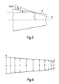
- Figure 5 is a schematic representation (not to scale) of part of a tapered waveguide 3 of a device according to the invention.
- the angle of taper ⁇ is indicated, this being the angle that the side surface of the waveguide makes with a line parallel to the longitudinal axis A of the waveguide.
- the adiabatic limit ⁇ A of the tapered waveguide is indicated, and this is an angle (also with respect to a line parallel to the longitudinal axis A) that is greater than the actual angle of taper by a constant angular separation C.A.S. as indicated in the figure.
- the angle of taper varies along the length of the tapered waveguide such that there are at least two changes in the angle of taper.
- a fifth aspect of the invention provides a device comprising a tapered semiconductor optical waveguide which tapers, at an angle of taper with respect to a longitudinal axis of the waveguide, from a relatively wide region to a relatively narrow region, wherein the angle of taper varies along the length of the tapered waveguide such that there are at least two changes in the angle of taper, and at all points along the taper the angle of taper is no greater than the adiabatic limit of the fundamental mode of the waveguide at that point along the taper.
- the invention provides a process of fabricating a device comprising a tapered semiconductor optical waveguide which tapers, at an angle of taper with respect to a longitudinal axis of the waveguide, from a relatively wide region to a relatively narrow region, the process comprising fabricating the tapered waveguide such that the angle of taper varies along the length of the tapered waveguide such that there at least two changes in the angle of taper, and at all points along the taper the angle of taper is no greater than the adiabatic limit of the fundamental mode of the waveguide at that point along the taper.
- the angle of taper may vary substantially continuously along the length of the waveguide (i.e. the taper is substantially continuously curved); in such embodiments the tapered waveguide effectively has an infinite number of changes in the angle of taper, along its length.
- the tapered waveguide preferably comprises a series of substantially straight tapered sections, each of which has a different angle of taper to that of its immediately neighbouring section(s). Such embodiments are preferred because their fabrication is generally easier than that of continuously curved tapers.
- FIG 6 is a schematic representation of a plan view of a tapered waveguide of a device according to the invention.
- the tapered waveguide shown comprises a modification (in accordance with the invention) of taper section BC of the known tapered rib waveguide shown in Figure 1.
- the modification comprises adjusting the angle of taper for each of eleven sections along the waveguide such that it is substantially at 0.05 degrees below the adiabatic limit for that section of the waveguide, as plotted in Figure 4 (the dotted line).
- width width/ ⁇ m section length/ ⁇ m Taper angle ( ⁇ )/degrees a 6.40 ab 98 0.105 b 6.04 bc 114 0.090 c 5.68 cd 131 0.077 d 5.33 de 158 0.065 e 4.97 ef 174 0.059 f 4.61 fg 166 0.062 g 4.25 gh 132 0.078 h 3.89 hi 92 0.109 i 3.54 ij 68 0.152 j 3.18 jk 54 0.191 k 2.82 kl 19 0.181 I 2.70
- the semiconductor of the waveguide according to the invention is silicon.
- the device may comprise a "silicon-on-insulator" device in which the tapered waveguide, and preferably one or more other waveguides and/or optical elements are fabricated in a layer of silicon overlying a layer of silica, which itself overlies a substrate, preferably also of silicon.
- the tapered waveguide is a rib waveguide, in which an elongate rib of the semiconductor stands proud of slab regions of the semiconductor on each side thereof.
- the invention is applicable to other types of waveguide, for example, ridge, channel, strip, etc, waveguides.
Landscapes
- Engineering & Computer Science (AREA)
- Physics & Mathematics (AREA)
- Power Engineering (AREA)
- Microelectronics & Electronic Packaging (AREA)
- General Physics & Mathematics (AREA)
- Optics & Photonics (AREA)
- Optical Integrated Circuits (AREA)
- Semiconductor Lasers (AREA)
Abstract
Description
| width | width/µm | section | length/µm | Taper angle ()/degrees | |
| a | 6.40 | ab | 98 | 0.105 | |
| b | 6.04 | bc | 114 | 0.090 | |
| c | 5.68 | cd | 131 | 0.077 | |
| d | 5.33 | de | 158 | 0.065 | |
| e | 4.97 | ef | 174 | 0.059 | |
| f | 4.61 | fg | 166 | 0.062 | |
| g | 4.25 | gh | 132 | 0.078 | |
| h | 3.89 | hi | 92 | 0.109 | |
| i | 3.54 | ij | 68 | 0.152 | |
| j | 3.18 | jk | 54 | 0.191 | |
| k | 2.82 | kl | 19 | 0.181 | |
| I | 2.70 |
Claims (16)
- A device comprising a tapered semiconductor optical waveguide which tapers, at an angle of taper with respect to a longitudinal axis of the waveguide, from a relatively wide region to a relatively narrow region, wherein the angle of taper varies along the length of the tapered waveguide such that at all points along the taper it is no greater than, and within a substantially constant angular separation of, the adiabatic limit of the fundamental mode of the waveguide at that point along the taper.
- A process of fabricating a device according to claim 1, comprising fabricating the tapered waveguide such that the angle of taper varies along the length of the tapered waveguide such that at all points along the taper it is no greater than, and within a constant angular separation of, the adiabatic limit of the fundamental mode of the waveguide at that point along the taper.
- A device according to claim 1, or a process according to claim 2, in which the angle of taper at all points along the taper is a said substantially constant angular separation below the adiabatic limit of the fundamental mode of the waveguide at that point along the taper.
- A device or process according to any preceding claim, in which said substantially constant angular separation is no greater than 80% of the adiabatic limit at any particular point along the taper.
- A device or process according to any preceding claim in which said substantially constant angular separation is at least 1.0% of the adiabatic limit at any particular point along the taper.
- A device or process according to any preceding claim, in which said substantially constant angular separation is in the range of 0.001 degrees to 0.1 degrees.
- A device or process according to any preceding claim, in which the angle of taper varies along the length of the tapered waveguide such that there are at least two changes in the angle of taper.
- A device comprising a tapered semiconductor optical waveguide which tapers, at an angle of taper with respect to a longitudinal axis of the waveguide, from a relatively wide region to a relatively narrow region, wherein the angle of taper varies along the length of the tapered waveguide such that there are at least two changes in the angle of taper, and at all points along the taper the angle of taper is no greater than the adiabatic limit of the fundamental mode of the waveguide at that point along the taper.
- A process of fabricating a device according to claim 8, comprising fabricating the tapered waveguide such that there are at least two changes in the angle of taper along the length of the tapered waveguide, and at all points along the taper the angle of taper is no greater than the adiabatic limit of the fundamental mode of the waveguide at that point along the taper.
- A device or process according to any preceding claim, in which there are at least three changes in the angle of taper along the length of the tapered waveguide.
- A device or process according to any preceding claim, in which there are at least four, preferably at least five, changes in the angle of taper along the length of the tapered waveguide.
- A device or process according to any preceding claim, in which the tapered waveguide comprises a series of substantially straight tapered sections, each of which has a different angle of taper to that of its immediately neighbouring section(s).
- A device or process according to any one of claims 1 to 11, in which the angle of taper varies substantially continuously along the length of the tapered waveguide.
- A device or process according to any preceding claim, in which the tapered waveguide is a rib waveguide
- A device or process according to any preceding claim, in which the semiconductor is silicon.
- A device or process according to any preceding claim, in which the relatively wide region of the tapered waveguide is a multimode region, and the relatively narrow region of the tapered waveguide is a single mode region.
Applications Claiming Priority (2)
| Application Number | Priority Date | Filing Date | Title |
|---|---|---|---|
| GB0212092A GB2388917A (en) | 2002-05-25 | 2002-05-25 | Semiconductor optical waveguide with a varying taper |
| GB0212092 | 2002-05-25 |
Publications (2)
| Publication Number | Publication Date |
|---|---|
| EP1369716A2 true EP1369716A2 (en) | 2003-12-10 |
| EP1369716A3 EP1369716A3 (en) | 2004-07-28 |
Family
ID=9937426
Family Applications (1)
| Application Number | Title | Priority Date | Filing Date |
|---|---|---|---|
| EP03011073A Withdrawn EP1369716A3 (en) | 2002-05-25 | 2003-05-20 | Tapered optical waveguide device in semiconductor |
Country Status (3)
| Country | Link |
|---|---|
| US (2) | US6853775B2 (en) |
| EP (1) | EP1369716A3 (en) |
| GB (1) | GB2388917A (en) |
Families Citing this family (14)
| Publication number | Priority date | Publication date | Assignee | Title |
|---|---|---|---|---|
| FR2936613B1 (en) * | 2008-09-30 | 2011-03-18 | Commissariat Energie Atomique | LIGHT COUPLER BETWEEN AN OPTICAL FIBER AND A WAVEGUIDE MADE ON A SOIL SUBSTRATE. |
| JP5933293B2 (en) * | 2012-03-01 | 2016-06-08 | 富士通株式会社 | Optical device, optical transmitter, optical receiver, optical transmitter / receiver, and method of manufacturing optical device |
| CN105264414B (en) * | 2013-06-07 | 2018-11-30 | 日本电气株式会社 | Waveguide Mode Converters, Polarizing Beam Splitters and Optical Devices |
| US9575251B1 (en) * | 2015-08-11 | 2017-02-21 | Oracle International Corporation | Optical mode converter having multiple regions |
| US9829626B2 (en) | 2016-01-13 | 2017-11-28 | Oracle International Corporation | Hybrid-integrated multi-chip module |
| WO2019180655A1 (en) | 2018-03-21 | 2019-09-26 | Ecole Polytechnique Federale De Lausanne (Epfl) | Optical coupling device |
| JP7135739B2 (en) * | 2018-11-01 | 2022-09-13 | 日本電信電話株式会社 | METHOD FOR MANUFACTURE OF SPOT SIZE CONVERTER AND SPOT SIZE CONVERTER |
| US10845669B2 (en) * | 2019-02-08 | 2020-11-24 | Ii-Vi Delaware Inc. | Vertical junction based silicon modulator |
| US11994715B2 (en) * | 2021-03-02 | 2024-05-28 | Rockley Photonics Limited | Compact waveguide taper and waveguide crossing |
| CN114114537B (en) * | 2021-12-08 | 2022-11-01 | 南通大学 | Design method of ultra-compact adiabatic tapered waveguide |
| CN115718347B (en) * | 2022-12-05 | 2023-06-27 | 南通大学 | Suitable for TE 1 And TE (TE) 3 Adiabatic mode switching connector for switching between modes |
| US20240219637A1 (en) | 2022-12-30 | 2024-07-04 | Openlight Photonics, Inc. | Thin silicon photonics with integrated iii-v waveguide |
| CN116449560B (en) * | 2023-04-04 | 2023-12-29 | 南通大学 | A reverse design method for adiabatic tapered waveguides in optical communications |
| CN116482856B (en) * | 2023-04-25 | 2024-01-26 | 南通大学 | Optimal design method of adiabatic mode converter in optical communication system |
Family Cites Families (12)
| Publication number | Priority date | Publication date | Assignee | Title |
|---|---|---|---|---|
| JPS58173704A (en) * | 1982-04-05 | 1983-10-12 | Matsushita Electric Ind Co Ltd | Optical focusing device |
| EP0495202B1 (en) * | 1991-01-15 | 1996-04-24 | Siemens Aktiengesellschaft | Device to change an optical wave with a small waist diameter into a wave with a bigger waist diameter |
| US5323476A (en) * | 1992-08-14 | 1994-06-21 | Siemens Aktiengesellschaft | Apparatus for increasing the cross section of optical waves |
| WO1994022038A1 (en) * | 1993-03-15 | 1994-09-29 | Telstra Corporation Limited | Improvements to optical waveguides |
| US5761364A (en) * | 1995-11-02 | 1998-06-02 | Motorola, Inc. | Optical waveguide |
| GB2317023B (en) * | 1997-02-07 | 1998-07-29 | Bookham Technology Ltd | A tapered rib waveguide |
| US6381380B1 (en) * | 1998-06-24 | 2002-04-30 | The Trustees Of Princeton University | Twin waveguide based design for photonic integrated circuits |
| US6470117B1 (en) * | 1998-12-04 | 2002-10-22 | Radiant Photonics, Inc. | Compression-molded three-dimensional tapered universal waveguide couplers |
| CA2258140C (en) * | 1999-01-06 | 2003-02-18 | Itf Optical Technologies Inc.-Technologies Optiques Itf Inc. | Optical fiber filters and method of making the same |
| US6293688B1 (en) * | 1999-11-12 | 2001-09-25 | Sparkolor Corporation | Tapered optical waveguide coupler |
| ATE256875T1 (en) * | 2001-03-29 | 2004-01-15 | Imec Inter Uni Micro Electr | TAPERED WAVEGUIDE (TAPER) WITH LATERAL BEAM-LIMITING RIBBED WAVEGUIDES |
| CA2354903C (en) * | 2001-08-08 | 2008-10-14 | Itf Technologies Optiques Inc./Itf Optical Technologies Inc. | Polarization-combining fused-fiber optical coupler and method of producing the same |
-
2002
- 2002-05-25 GB GB0212092A patent/GB2388917A/en not_active Withdrawn
-
2003
- 2003-05-20 EP EP03011073A patent/EP1369716A3/en not_active Withdrawn
- 2003-05-22 US US10/444,862 patent/US6853775B2/en not_active Expired - Fee Related
-
2005
- 2005-02-04 US US11/051,070 patent/US7035509B2/en not_active Expired - Lifetime
Also Published As
| Publication number | Publication date |
|---|---|
| EP1369716A3 (en) | 2004-07-28 |
| US20040037506A1 (en) | 2004-02-26 |
| GB2388917A (en) | 2003-11-26 |
| US7035509B2 (en) | 2006-04-25 |
| US6853775B2 (en) | 2005-02-08 |
| GB0212092D0 (en) | 2002-07-03 |
| US20050244104A1 (en) | 2005-11-03 |
Similar Documents
| Publication | Publication Date | Title |
|---|---|---|
| CN1146736C (en) | wedge rib waveguide | |
| EP1356327B1 (en) | Optical mode size converter with vertical and horizontal mode shaping | |
| EP0731366B1 (en) | Twodimensional segmentation of an integrated optics waveguide to match the waveguide's mode to that of a fibre | |
| US6853775B2 (en) | Semiconductor optical waveguide device | |
| EP0731367B1 (en) | Integrated optic waveguide with side gaps of increasing depth to match the waveguide's mode to that of a fibre | |
| US7668416B2 (en) | Single mode photonic circuit architecture and a new optical splitter design based on parallel waveguide mode conversion | |
| US6169825B1 (en) | Integrated optical polarizer | |
| EP1189084B1 (en) | Planar lightwave circuit and optical circuit | |
| US6571039B1 (en) | Optical waveguide having a weakly-confining waveguide section and a strongly-confining waveguide section optically coupled by a tapered neck | |
| US6643432B2 (en) | Optical waveguide device and optical waveguide method | |
| EP0645650B1 (en) | Integrated optical polarization converter with enhanced periodic coupling | |
| EP0629297A1 (en) | Integrated optical component. | |
| EP1555551B1 (en) | Apparatus for compactly coupling an optical fiber and a planar optical waveguide | |
| US20050089291A1 (en) | Waveguide structure and method of manufacturing the same | |
| US20050185893A1 (en) | Method and apparatus for tapering an optical waveguide | |
| KR20230158396A (en) | Back-end-of-line edge couplers with a tapered grating | |
| US7088889B2 (en) | Optical splitter | |
| KR102891313B1 (en) | Edge couplers including a metamaterial layer | |
| CN1474952A (en) | Birefringence Control in Optical Waveguides and Sequential Waveguide Gratings | |
| Shinya et al. | Functional components in SOI photonic crystal slabs | |
| Harpin | Integrated optics in silicon: coming of age | |
| Chen et al. | Vertical tapered mode size transformer in polymer waveguides for efficient fiber coupling | |
| HK1026271A (en) | A tapered rib waveguide | |
| US20060093298A1 (en) | Integrated optical waveguide and process for fabrication |
Legal Events
| Date | Code | Title | Description |
|---|---|---|---|
| PUAI | Public reference made under article 153(3) epc to a published international application that has entered the european phase |
Free format text: ORIGINAL CODE: 0009012 |
|
| AK | Designated contracting states |
Kind code of ref document: A2 Designated state(s): AT BE BG CH CY CZ DE DK EE ES FI FR GB GR HU IE IT LI LU MC NL PT RO SE SI SK TR |
|
| AX | Request for extension of the european patent |
Extension state: AL LT LV MK |
|
| PUAL | Search report despatched |
Free format text: ORIGINAL CODE: 0009013 |
|
| AK | Designated contracting states |
Kind code of ref document: A3 Designated state(s): AT BE BG CH CY CZ DE DK EE ES FI FR GB GR HU IE IT LI LU MC NL PT RO SE SI SK TR |
|
| AX | Request for extension of the european patent |
Extension state: AL LT LV MK |
|
| RIC1 | Information provided on ipc code assigned before grant |
Ipc: 7G 02B 6/12 B Ipc: 7G 02B 6/30 B Ipc: 7G 02B 6/122 A |
|
| AKX | Designation fees paid | ||
| REG | Reference to a national code |
Ref country code: DE Ref legal event code: 8566 |
|
| STAA | Information on the status of an ep patent application or granted ep patent |
Free format text: STATUS: THE APPLICATION IS DEEMED TO BE WITHDRAWN |
|
| 18D | Application deemed to be withdrawn |
Effective date: 20050129 |