EP1367761A1 - Measurement of jitter in digital communications signals - Google Patents
Measurement of jitter in digital communications signals Download PDFInfo
- Publication number
- EP1367761A1 EP1367761A1 EP02253762A EP02253762A EP1367761A1 EP 1367761 A1 EP1367761 A1 EP 1367761A1 EP 02253762 A EP02253762 A EP 02253762A EP 02253762 A EP02253762 A EP 02253762A EP 1367761 A1 EP1367761 A1 EP 1367761A1
- Authority
- EP
- European Patent Office
- Prior art keywords
- jitter
- measurement
- pass filter
- communications signal
- samples
- Prior art date
- Legal status (The legal status is an assumption and is not a legal conclusion. Google has not performed a legal analysis and makes no representation as to the accuracy of the status listed.)
- Granted
Links
- 238000005259 measurement Methods 0.000 title claims abstract description 81
- 238000004891 communication Methods 0.000 title claims abstract description 22
- 230000006870 function Effects 0.000 claims abstract description 38
- 238000000034 method Methods 0.000 claims description 10
- 238000012545 processing Methods 0.000 description 7
- 238000012360 testing method Methods 0.000 description 6
- 238000001914 filtration Methods 0.000 description 4
- 238000013461 design Methods 0.000 description 3
- 238000010586 diagram Methods 0.000 description 3
- 230000004044 response Effects 0.000 description 3
- 238000009825 accumulation Methods 0.000 description 2
- 238000004458 analytical method Methods 0.000 description 2
- 230000000694 effects Effects 0.000 description 2
- 238000007781 pre-processing Methods 0.000 description 2
- 230000001360 synchronised effect Effects 0.000 description 2
- 102100032467 Transmembrane protease serine 13 Human genes 0.000 description 1
- 238000013459 approach Methods 0.000 description 1
- 230000008901 benefit Effects 0.000 description 1
- 230000005540 biological transmission Effects 0.000 description 1
- 230000001419 dependent effect Effects 0.000 description 1
- 238000001514 detection method Methods 0.000 description 1
- 230000009977 dual effect Effects 0.000 description 1
- 238000000765 microspectrophotometry Methods 0.000 description 1
- 238000012544 monitoring process Methods 0.000 description 1
- 235000019799 monosodium phosphate Nutrition 0.000 description 1
- 230000003287 optical effect Effects 0.000 description 1
- 230000002093 peripheral effect Effects 0.000 description 1
- 230000008569 process Effects 0.000 description 1
- 238000013139 quantization Methods 0.000 description 1
- 238000011084 recovery Methods 0.000 description 1
- 230000009467 reduction Effects 0.000 description 1
- 238000005070 sampling Methods 0.000 description 1
- 238000012883 sequential measurement Methods 0.000 description 1
- 238000004088 simulation Methods 0.000 description 1
- 239000013598 vector Substances 0.000 description 1
Images


Classifications
-
- H—ELECTRICITY
- H04—ELECTRIC COMMUNICATION TECHNIQUE
- H04L—TRANSMISSION OF DIGITAL INFORMATION, e.g. TELEGRAPHIC COMMUNICATION
- H04L1/00—Arrangements for detecting or preventing errors in the information received
- H04L1/20—Arrangements for detecting or preventing errors in the information received using signal quality detector
- H04L1/205—Arrangements for detecting or preventing errors in the information received using signal quality detector jitter monitoring
Definitions
- This invention relates to methods and apparatus for measuring jitter affecting digital signals used for transmitting information in communications networks.
- Digital communications networks are continuing to grow relentlessly in extent and capacity, and to become increasingly pervasive in the social and business infrastructure of many countries. Consequently test and measurement equipment for assisting monitoring and management of such networks to avoid interruption of their operation is crucially important.
- timing jitter is defined in publications of the International Telecommunications Union (ITU) as "short-term variations of the significant instances of a digital signal from their ideal positions in time (where short-term implies these variations are of frequency greater than or equal to 10 Hz)". Limits are specified in various international standards (e.g. ITU-T Recommendations G.823, G.824 and G.825) for maximum permissible levels of jitter at interfaces within a digital network.
- limits are specified in pairs, one for a measurement using a wide-band measurement filter and one using a high-band measurement filter (with a lower cut-off frequency which is above that of the wide-band filter, and with the same minimum upper cut-off frequency).
- the wide-band filter's lower cut-off frequency is chosen in accordance with the characteristics of timing circuits (e.g. implemented as either phase-locked loops or high-pass filters) which may be incorporated in network equipment.
- the high-band filter's lower cut-off frequency is related to the bandwidth of input timing acquisition circuitry.
- the minimum upper cut-off frequency is chosen to reflect reasonable measurement limitations and to include all expected, significant alignment jitter.
- the required measurement bandwidth is implemented by using a fixed low-pass, wide-band filter for one measurement and switching in a high-pass filter for the other measurement. An additional RMS jitter measurement is performed using a third high pass filter selection.
- Network equipment can typically be configured to operate at any one of several different rates of transmission of data symbols (line rates), in a hierarchy of related rates such as those specified in the SONET (Synchronous Optical Network) and SDH (Synchronous Digital Hierarchy) systems.
- line rates have respective pairs of wide-band and high-band measurement bandwidths specified, usually requiring respective high-pass filters which are switched in to enable one or both of the two measurements to be made for a particular line rate.
- For each line rate there is also a different low pass filter. For certain purposes measurements at bandwidths additional to those required by the standards may be desirable.
- a jitter measurement test usually takes several minutes. Therefore completing measurements for all filter combinations desired for a given line rate can be very time consuming.
- a method of measuring jitter in a digital communications signal comprising the steps of:
- apparatus for measuring jitter in a digital communications signal comprising:
- the circuitry shown in the drawings implements five high-pass filter functions and a parallel, through-path which operate simultaneously so the jitter data in six different measurement bandwidths is available simultaneously.
- the parallel processing capabilities of an FPGA are used to provide digital high-pass filter banks, and also provide low-pass filtering for some line rates. This is advantageous in comparison to analogue filters which typically exhibit some variation in filter characteristic from unit to unit, requiring careful design and setup adjustments to compensate.
- a large area of circuitry would be required to implement several different bandwidth options using analogue components, leading to a physically bulky and awkward equipment.
- an analogue implementation to provide simultaneous measurement results would require multiple, costly analogue-to-digital converters (ADCs) in parallel and associated peripheral components.
- ADCs analogue-to-digital converters
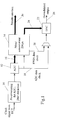
- a clock signal from a device under test is supplied to a pre-processing circuit 10 which prepares the signal for input to an ADC 12.
- This pre-processing includes for example phase detection to extract the jitter component of the clock signal, and filtering for anti-aliasing.
- the ADC 12 samples the input signal at a suitable sample rate, dependent on the jitter measurement bandwidth, and provides 12-bit digitised values of the successive samples to a filter/measurement FPGA 14 via a parallel data bus 16, together with a data clock signal on a line 18.
- the FPGA 14 filters and measures the samples as described in more detail below, so that the required jitter measurements can be derived and output on a parallel results bus interface 20 for display, further processing etc.
- Selected samples as filtered by the FPGA 14 are also output to a digital-to-analogue converter (DAC) 22 via a parallel bus 24, together with a clock signal on a line 26, so that a demodulated signal representative of the jitter in the signal from the DUT can be output on a line 28.
- DAC digital-to-analogue converter
- the FPGA implements five parallel high-pass filter functions.
- the output of each filter and of a through-path is processed by a peak-to-peak measurement module, a root-mean-square (RMS) measurement module and a jitter peak occurrence (hit) counter module within the FPGA.
- RMS root-mean-square
- hit jitter peak occurrence
- the sample values output by the ADC on the data bus 16 are fed to a first of a pair of selectors 30 and 32 for selecting either of two post-emphasis filters 34 and 36 with filter characteristics H21 and H22 respectively, which compensate for clock recovery frequency response effects.
- the selectors 30 and 32 can also feed the received data samples directly from one to the other, to bypass the post-emphasis filtering.
- the data samples emerging from the selector 32 are passed through a filter 38, implementing the low-pass filtering function required by the ITU Recommendations, to a bank 40 of digital high-pass filter functions.
- This bank comprises five filter functions 40(i) to 40(v) together with a through path 40(vi).
- the filter functions 40(iii) and 40(v) implement the high-band measurement bandwidths required by the ITU Recommendations for the line rate being tested.
- the functions 40(i), 40(ii) and 40(iv) provide a third bandwidth for RMS jitter measurements and two further bandwidths which are considered to be useful to provide additional versatility in a jitter test environment.
- the data samples from the filter 38 are supplied to all the filter functions 40(i) to 40(vi) simultaneously.
- the outputs from the high-pass filter functions and the through path are connected to a latency adjustment circuit 42, to ensure that the filter delay for a given sample is the same for each path and the parallel measurements are therefore simultaneous, and from there to a measurement block 44.
- the measurement block 44 implements six sets of measurement functions, each set comprising an RMS integrator, positive peak detector, negative peak detector, positive peak occurrence counter and negative peak occurrence counter. Each of these six sets of measurement functions is coupled to a respective high-pass filter function or the through path in the bank 40 via a respective path through the latency adjustment circuit 42, so that data processing for the measurement functions implemented in the block 44 proceeds for all six filter functions in the bank 40 simultaneously.
- the measurement block 40 accumulates measurement information over a succession of measurement intervals, and the results of the data processing at the end of each measurement interval are supplied by the measurement block 44 via the results interface 20 to an instrument processor for reporting of the required jitter measurements in conventional manner.
- All the results collected during one measurement interval are available for display while the measurement results for the following interval are being accumulated.
- the jitter measurements for one, several or all of the high-pass filter functions 40 may be displayed simultaneously. Changes in display choices can be performed without any delay for gathering of the related measurements.
- Data are supplied to the DAC 22 ( Figure 1) via the bus 24 from the circuit 42, which connects one of the outputs from the high-pass filter bank 40 to the bus 24 in accordance with a user selection.
- the digital filter implementations used for the high-pass filter functions 40 incorporate relatively wide (32-bit) data words to provide filter roll-off accuracy and measurement resolution.
- the filters are implemented as recursive infinite impulse response (IIR) filters to minimize the requirement for FPGA capacity.
- FIG. 3 the input data for the feedback stage are supplied to an input circuit 46 which is coupled to a first commutator 48 which switches repetitively between two states at the sample data rate. In a first state the received data are fed through a first feedback path 50, implementing the required IIR feedback operation. In the commutator's second state the data are fed to a second feedback path 52, implementing the same feedback function. The outputs of the two feedback paths 50 and 52 are coupled to a second commutator 54 operating synchronously with the first commutator 48.
- the Y(n) summation is performed in the input stage 46 and can be done at full rate as it is a feed forward circuit and can be pipelined.
- the X(n) summation is accomplished over two sample periods, using the two multiplexed parallel feedback paths 50 and 52.
- k 2 is implemented as a fixed coefficient. Some approximation occurs owing to quantization of the k 2 term. However, the feedback loop only operates every two samples, reducing the accumulation of such error. This reduction in error accumulation has a more dominant effect on the accuracy of the filter response than the approximation error.
- a set of mathematical software modelling programs are used to design and analyse a bank of high pass filters over a range of possible data sample rates.
- the programs also analyse the filters at each data rate to identify the number of summation operations required to create a 'sum of bit-shifted inputs' implementation of the coefficient multiplier.
- Some sample frequencies could only be used if the coefficients are implemented using a large number of summations, so these frequencies are preferably avoided.
- the results of this modelling are inspected to identify a sample frequency that offers optimum accuracy, whilst allowing the simplest coefficients (least number of bits) to be used.
- the filter designs are simulated using a true fixed point simulator.
- the simulation results data are used as the FPGA test vectors.
- the jitter measurement circuitry described above enables jitter measurement equipment to make multiple, simultaneous jitter measurements at different measurement bandwidths of a communications signal at a selected line rate, thereby effecting a substantial saving in time over previous sequential measurement approaches.
Landscapes
- Engineering & Computer Science (AREA)
- Quality & Reliability (AREA)
- Computer Networks & Wireless Communication (AREA)
- Signal Processing (AREA)
- Dc Digital Transmission (AREA)
Abstract
Description
- Figure 1
- is a block schematic diagram of principal components of jitter measurement circuitry;
- Figure 2
- is a block schematic diagram of filter and measurement functionality implemented in a field programmable gate array (FPGA) forming part of the circuitry of Figure 1; and
- Figure 3
- is a block schematic diagram of a parallel feedback processing function incorporated in the FPGA of Figure 2.
- The data rate required to sample the full jitter measurement bandwidth accurately (e.g. 204 MSPs) is very fast, such that, in conjunction with the 32-bit wide data words, the fastest available FPGA could not perform the feedback operation required (32 x 32 bit, fixed coefficient multiplication) for an IIR filter within one sample period.
- Some of the high-pass filters have very low cut-off frequencies in relation to the data sampling rate, such that they could almost be considered as DC stops. However, the relevant jitter measurement standards require that the filters provide a 1st order Butterworth roll-off characteristic, and that the cut-off frequency meets a specified tolerance, so a simple DC stop filter could not be used. The coefficient values comprising the definition of the digital filter functions therefore have to be very accurate.
- In selecting multiplier coefficients for a digital filter, it is advantageous to be able to select a data sample rate that is related to the coefficients so as to reduce the coefficient multiplication operations to single and dual bit operations. More complex multiplication operations would require extra FPGA capacity, and would reduce the maximum speed at which the FPGA can perform the coefficient multiplication operations. In implementing a bank of filters operating simultaneously a data rate is selected to suit all the filters.
u(n) is the input to the feedback path for the nth sample; and
k is a constant feedback factor.
Considered over two sample periods this becomes:
Claims (7)
- A method of measuring jitter in a digital communications signal, comprising the steps of:generating multiple successive samples representative of jitter in a digital communications signal;supplying the successive samples in parallel to a plurality of high-pass filter functions to generate filtered samples;supplying the filtered samples from each high-pass filter function to a respective one of a plurality of measurement functions, for measurement of parameters of the filtered samples from the corresponding high-pass filter function, the parameters comprising jitter peak amplitude and jitter RMS amplitude; andselecting parameter measurements provided by the measurement functions and deriving therefrom a measurement of jitter in the communications signal.
- The method of claim 1, wherein the measured parameters include a count of jitter peak occurrences over a predetermined time interval.
- The method of claim 2, wherein the measured parameters include a count of jitter positive and negative peak occurrences over the predetermined time interval.
- The method of any of the preceding claims, wherein the measured parameters include positive and negative jitter peak amplitudes.
- The method of claim 1, wherein all measurements of jitter for a plurality of the high-pass filter functions are available for display simultaneously.
- The method of any of the preceding claims, wherein one of the high-pass filter functions is a through path filter function.
- Apparatus for measuring jitter in a digital communications signal, comprising:a generator for generating multiple successive samples representative of jitter in a digital communications signal;a plurality of high-pass filters for receiving the successive samples in parallel to generate filtered samples;for each high-pass filter, a respective plurality of measurement circuits for receiving and measuring parameters of the filtered samples from that high-pass filter, the parameters comprising jitter peak amplitude and jitter RMS amplitude; anda selector for selecting parameter measurements provided by the measurement circuits and deriving therefrom a measurement of jitter in the communications signal.
Priority Applications (4)
| Application Number | Priority Date | Filing Date | Title |
|---|---|---|---|
| EP02253762A EP1367761B1 (en) | 2002-05-29 | 2002-05-29 | Measurement of jitter in digital communications signals |
| DE60217649T DE60217649T2 (en) | 2002-05-29 | 2002-05-29 | Dither measurement in digital communication signals |
| JP2003150124A JP2004029013A (en) | 2002-05-29 | 2003-05-28 | Digital communication signal jitter measurement method |
| US10/447,139 US20030223487A1 (en) | 2002-05-29 | 2003-05-29 | Measurement of jitter in digital communications signals |
Applications Claiming Priority (1)
| Application Number | Priority Date | Filing Date | Title |
|---|---|---|---|
| EP02253762A EP1367761B1 (en) | 2002-05-29 | 2002-05-29 | Measurement of jitter in digital communications signals |
Publications (2)
| Publication Number | Publication Date |
|---|---|
| EP1367761A1 true EP1367761A1 (en) | 2003-12-03 |
| EP1367761B1 EP1367761B1 (en) | 2007-01-17 |
Family
ID=29414814
Family Applications (1)
| Application Number | Title | Priority Date | Filing Date |
|---|---|---|---|
| EP02253762A Expired - Lifetime EP1367761B1 (en) | 2002-05-29 | 2002-05-29 | Measurement of jitter in digital communications signals |
Country Status (4)
| Country | Link |
|---|---|
| US (1) | US20030223487A1 (en) |
| EP (1) | EP1367761B1 (en) |
| JP (1) | JP2004029013A (en) |
| DE (1) | DE60217649T2 (en) |
Families Citing this family (5)
| Publication number | Priority date | Publication date | Assignee | Title |
|---|---|---|---|---|
| US7545858B2 (en) * | 2004-06-29 | 2009-06-09 | Agilent Technologies, Inc. | Method of measuring jitter frequency response |
| US7239969B2 (en) | 2004-11-09 | 2007-07-03 | Guide Technology, Inc. | System and method of generating test signals with injected data-dependent jitter (DDJ) |
| GB2463260B (en) * | 2008-09-05 | 2012-09-12 | Phabrix Ltd | Jitter Evaluation |
| JP6164680B2 (en) | 2012-12-27 | 2017-07-19 | リーダー電子株式会社 | Method and apparatus for generating jitter-related data |
| US9172428B2 (en) * | 2013-06-28 | 2015-10-27 | Intel Corporation | Determining the spectral energy content of a data bus |
Citations (1)
| Publication number | Priority date | Publication date | Assignee | Title |
|---|---|---|---|---|
| US5757652A (en) * | 1995-12-21 | 1998-05-26 | Tektronix, Inc. | Electrical signal jitter and wander measurement system and method |
Family Cites Families (6)
| Publication number | Priority date | Publication date | Assignee | Title |
|---|---|---|---|---|
| US3676583A (en) * | 1969-08-13 | 1972-07-11 | Victor Company Of Japan | Jitter correction system |
| US4149044A (en) * | 1978-01-10 | 1979-04-10 | Hekimian Norris C | Method and apparatus for graphically displaying amplitude and phase jitter |
| US4975634A (en) * | 1989-04-07 | 1990-12-04 | General Signal Corporation | Jitter measurement device |
| GB2368651B (en) * | 2000-10-31 | 2006-05-31 | Consultronics Europ Ltd | Method and apparatus for measurement of jitter |
| WO2003044543A2 (en) * | 2001-08-22 | 2003-05-30 | Wavecrest Corporation | Method and apparatus for measuring a waveform |
| JP3790741B2 (en) * | 2002-12-17 | 2006-06-28 | アンリツ株式会社 | Jitter measuring apparatus and jitter measuring method |
-
2002
- 2002-05-29 EP EP02253762A patent/EP1367761B1/en not_active Expired - Lifetime
- 2002-05-29 DE DE60217649T patent/DE60217649T2/en not_active Expired - Fee Related
-
2003
- 2003-05-28 JP JP2003150124A patent/JP2004029013A/en active Pending
- 2003-05-29 US US10/447,139 patent/US20030223487A1/en not_active Abandoned
Patent Citations (1)
| Publication number | Priority date | Publication date | Assignee | Title |
|---|---|---|---|---|
| US5757652A (en) * | 1995-12-21 | 1998-05-26 | Tektronix, Inc. | Electrical signal jitter and wander measurement system and method |
Non-Patent Citations (2)
| Title |
|---|
| ITU-T: "The control of jitter and wander within digital networks which are based on the 1544 kbit/s hierarchy", ITU-T RECOMMENDATION G.824, March 2000 (2000-03-01), Geneva, CH, XP002223720 * |
| ITU-T: "The control of jitter and wander within digital networks which are based on the synchronous digital hierarchy (SDH)", ITU-T RECOMMENDATION G.825, March 2000 (2000-03-01), Geneva, CH, XP002223721 * |
Also Published As
| Publication number | Publication date |
|---|---|
| US20030223487A1 (en) | 2003-12-04 |
| EP1367761B1 (en) | 2007-01-17 |
| JP2004029013A (en) | 2004-01-29 |
| DE60217649D1 (en) | 2007-03-08 |
| DE60217649T2 (en) | 2007-05-24 |
Similar Documents
| Publication | Publication Date | Title |
|---|---|---|
| US7236555B2 (en) | Method and apparatus for measuring jitter | |
| SE516135C2 (en) | Method and apparatus for digitizing a signal with large frequency bandwidth | |
| EP0941480B1 (en) | Measurement instrument amplitude calibration | |
| US5650951A (en) | Programmable data acquisition system with a microprocessor for correcting magnitude and phase of quantized signals while providing a substantially linear phase response | |
| EP1367761B1 (en) | Measurement of jitter in digital communications signals | |
| US4689759A (en) | Process and installation for the analysis and retrieval of a sampling and interpolation signal | |
| CN113009201B (en) | Electric signal sampling device | |
| WO2003044543A2 (en) | Method and apparatus for measuring a waveform | |
| US20040213565A1 (en) | Method and apparatus for optical signal and noise analysis using pulse amplitude histogram | |
| CN117538588A (en) | Amplitude-frequency response and phase-frequency response compensation device, compensation method and oscilloscope | |
| CN114545078B (en) | Intermediate frequency signal processing system and processing method | |
| US6961520B2 (en) | Method for measurement of optical or electrical signal sequences and eye diagram monitor for measurement and display of signal sequences | |
| EP1475641B1 (en) | Method and device for precise measurement of dependency on amplitude and phase of plurality of high frequency signals | |
| JP2000221248A (en) | Semiconductor test equipment | |
| CN118068063A (en) | Oscilloscope | |
| JP2003004782A (en) | Network measurement method and device | |
| CN120908516B (en) | A high-voltage pulse calibration method and system based on distributed deployment | |
| Pickerd | DSP in high performance oscilloscopes | |
| CN112213625B (en) | Automatic temperature experiment test method and device for signal generation plate | |
| García et al. | An 8 GHz digital spectrometer for millimeter-wave astronomy | |
| CN100502261C (en) | Method for testing analog channel suppressing degree of receiver | |
| CN119087007B (en) | Broadband digital triggering system, method and related electronic equipment | |
| Pawłowski et al. | Programmable, switched-capacitor finite impulse response filter realized in CMOS technology for education purposes | |
| JP2010256123A (en) | Transmission path evaluation method, transmission path evaluation system, and transmission path modeling apparatus | |
| Comoretto et al. | Radioastronomic signal processing cores for the SKA radio telescope |
Legal Events
| Date | Code | Title | Description |
|---|---|---|---|
| PUAI | Public reference made under article 153(3) epc to a published international application that has entered the european phase |
Free format text: ORIGINAL CODE: 0009012 |
|
| AK | Designated contracting states |
Kind code of ref document: A1 Designated state(s): AT BE CH CY DE DK ES FI FR GB GR IE IT LI LU MC NL PT SE TR |
|
| AX | Request for extension of the european patent |
Extension state: AL LT LV MK RO SI |
|
| 17P | Request for examination filed |
Effective date: 20040603 |
|
| AKX | Designation fees paid |
Designated state(s): DE FR GB |
|
| 17Q | First examination report despatched |
Effective date: 20041118 |
|
| GRAP | Despatch of communication of intention to grant a patent |
Free format text: ORIGINAL CODE: EPIDOSNIGR1 |
|
| GRAS | Grant fee paid |
Free format text: ORIGINAL CODE: EPIDOSNIGR3 |
|
| GRAA | (expected) grant |
Free format text: ORIGINAL CODE: 0009210 |
|
| AK | Designated contracting states |
Kind code of ref document: B1 Designated state(s): DE FR GB |
|
| REG | Reference to a national code |
Ref country code: GB Ref legal event code: FG4D |
|
| RAP2 | Party data changed (patent owner data changed or rights of a patent transferred) |
Owner name: AGILENT TECHNOLOGIES, INC. |
|
| REF | Corresponds to: |
Ref document number: 60217649 Country of ref document: DE Date of ref document: 20070308 Kind code of ref document: P |
|
| PGFP | Annual fee paid to national office [announced via postgrant information from national office to epo] |
Ref country code: DE Payment date: 20070702 Year of fee payment: 6 |
|
| PLBE | No opposition filed within time limit |
Free format text: ORIGINAL CODE: 0009261 |
|
| STAA | Information on the status of an ep patent application or granted ep patent |
Free format text: STATUS: NO OPPOSITION FILED WITHIN TIME LIMIT |
|
| 26N | No opposition filed |
Effective date: 20071018 |
|
| PG25 | Lapsed in a contracting state [announced via postgrant information from national office to epo] |
Ref country code: FR Free format text: LAPSE BECAUSE OF FAILURE TO SUBMIT A TRANSLATION OF THE DESCRIPTION OR TO PAY THE FEE WITHIN THE PRESCRIBED TIME-LIMIT Effective date: 20070907 |
|
| PG25 | Lapsed in a contracting state [announced via postgrant information from national office to epo] |
Ref country code: FR Free format text: LAPSE BECAUSE OF FAILURE TO SUBMIT A TRANSLATION OF THE DESCRIPTION OR TO PAY THE FEE WITHIN THE PRESCRIBED TIME-LIMIT Effective date: 20070117 |
|
| PGFP | Annual fee paid to national office [announced via postgrant information from national office to epo] |
Ref country code: GB Payment date: 20080604 Year of fee payment: 7 |
|
| PG25 | Lapsed in a contracting state [announced via postgrant information from national office to epo] |
Ref country code: DE Free format text: LAPSE BECAUSE OF NON-PAYMENT OF DUE FEES Effective date: 20081202 |
|
| GBPC | Gb: european patent ceased through non-payment of renewal fee |
Effective date: 20090529 |
|
| PG25 | Lapsed in a contracting state [announced via postgrant information from national office to epo] |
Ref country code: GB Free format text: LAPSE BECAUSE OF NON-PAYMENT OF DUE FEES Effective date: 20090529 |