EP1367712A2 - Amplifier and radio frequency tuner - Google Patents
Amplifier and radio frequency tuner Download PDFInfo
- Publication number
- EP1367712A2 EP1367712A2 EP03101451A EP03101451A EP1367712A2 EP 1367712 A2 EP1367712 A2 EP 1367712A2 EP 03101451 A EP03101451 A EP 03101451A EP 03101451 A EP03101451 A EP 03101451A EP 1367712 A2 EP1367712 A2 EP 1367712A2
- Authority
- EP
- European Patent Office
- Prior art keywords
- amplifier
- stage
- input
- output
- transistors
- Prior art date
- Legal status (The legal status is an assumption and is not a legal conclusion. Google has not performed a legal analysis and makes no representation as to the accuracy of the status listed.)
- Granted
Links
Images


Classifications
-
- H—ELECTRICITY
- H03—ELECTRONIC CIRCUITRY
- H03F—AMPLIFIERS
- H03F1/00—Details of amplifiers with only discharge tubes, only semiconductor devices or only unspecified devices as amplifying elements
- H03F1/26—Modifications of amplifiers to reduce influence of noise generated by amplifying elements
-
- H—ELECTRICITY
- H03—ELECTRONIC CIRCUITRY
- H03F—AMPLIFIERS
- H03F3/00—Amplifiers with only discharge tubes or only semiconductor devices as amplifying elements
- H03F3/189—High-frequency amplifiers, e.g. radio frequency amplifiers
- H03F3/19—High-frequency amplifiers, e.g. radio frequency amplifiers with semiconductor devices only
- H03F3/195—High-frequency amplifiers, e.g. radio frequency amplifiers with semiconductor devices only in integrated circuits
-
- H—ELECTRICITY
- H03—ELECTRONIC CIRCUITRY
- H03F—AMPLIFIERS
- H03F3/00—Amplifiers with only discharge tubes or only semiconductor devices as amplifying elements
- H03F3/45—Differential amplifiers
- H03F3/45071—Differential amplifiers with semiconductor devices only
- H03F3/45076—Differential amplifiers with semiconductor devices only characterised by the way of implementation of the active amplifying circuit in the differential amplifier
- H03F3/4508—Differential amplifiers with semiconductor devices only characterised by the way of implementation of the active amplifying circuit in the differential amplifier using bipolar transistors as the active amplifying circuit
- H03F3/45085—Long tailed pairs
-
- H—ELECTRICITY
- H03—ELECTRONIC CIRCUITRY
- H03F—AMPLIFIERS
- H03F2200/00—Indexing scheme relating to amplifiers
- H03F2200/294—Indexing scheme relating to amplifiers the amplifier being a low noise amplifier [LNA]
-
- H—ELECTRICITY
- H03—ELECTRONIC CIRCUITRY
- H03F—AMPLIFIERS
- H03F2200/00—Indexing scheme relating to amplifiers
- H03F2200/372—Noise reduction and elimination in amplifier
Definitions
- the present invention relates to an amplifier, for example for use as a low noise amplifier (LNA) in a radio frequency tuner.
- the present invention also relates to a radio frequency tuner including such an amplifier.
- LNA low noise amplifier
- an amplifier comprising an inverting amplifier stage having an input connected via an input resistance to an input of the amplifier and via a feedback resistance to an output of the amplifier stage characterised by comprising a transconductance stage for passing through the input resistance a current substantially proportional to the output voltage of the amplifier stage.
- the amplifier stage may comprise a common emitter or common source transistor.
- the amplifier may comprise a low noise amplifier.
- a radio frequency tuner comprising an amplifier according to the first aspect of the invention.
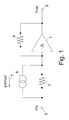
- the amplifier shown in Figure 1 is suitable for use as an LNA ahead of a frequency changer or a first frequency changer of a radio frequency tuner.
- the amplifier comprises an amplifier stage 1 whose input is connected via an input resistor 2 to an input 3 of the amplifier and via a resistor 4 to an output of the amplifier stage, which is also connected to an output 5 of the amplifier.
- the amplifier stage 1 has an open loop gain -A.
- the amplifier also comprises a transconductance stage illustrated diagrammatically at 6 and having a transconductance gm.
- the amplifier receives an input signal Vin at the input 3 and supplies an output Vout at the output 5.
- the transconductance stage 6 converts the output voltage of the amplifier stage 1 to a current gm.Vout, which is applied across the input resistor 2.
- An arrow 6 indicates the output phase of the transconductance stage 6 such that the output current gm.Vout is applied to the terminal of the resistor 2 connected to the input 3 with respect to the other terminal of the resistor 2 connected to
- Vin (1 gm.A. Rf 1 + A . Rin.i + i Rf 1 + A
- the gain A of the amplifier stage 1 is arranged to be relatively large and, as A tends to infinity, the expression for the input voltage Vin may be rewritten as:
- the value Rin of the input resistor 2 may be set to 10 ohms and the factor (1+ ⁇ ) may be set to 10. This gives an input impedance of 100 ohms and an S1 1 of - 17dB.
- the noise figure of the amplifier is dominated by the resistance Rin of the input resistor 2 and by the contribution of noise from the base spreading resistance Rbb and the base current shot noise of the input stage of the amplifier stage 1.
- the transconductance stage 6 may be implemented with resistors having values at least five times that of Rin, which gives rise to low current noise so that the noise contribution of the transconductance stage 6 is negligible.
- the noise figure of the whole amplifier may be reduced to 3dB while maintaining S11 at approximately -20dB and IIP3 at substantially +20dBm.
- the amplifier stage 1 comprises a common emitter input amplifying stage and an emitter follower output stage.
- the input stage comprises an NPN bipolar junction transistor 10 having a collector load in the form of a constant current source 11 connected to a positive power supply line 12.
- the emitter of the transistor 10 is connected to ground gnd via a resistor 13, which is bypassed at signal frequencies by a capacitor 14.
- the collector of the transistor 10 is connected to the emitter follower output stage comprising an NPN bipolar junction transistor 15 whose emitter load comprises a constant current source 16.
- the transconductance stage 6 comprises a long tail pair of NPN bipolar junction transistors 17 and 18, whose emitters are connected via emitter degeneration resistors 19 and 20, respectively, to a constant tail current source 21.
- the collector of the transistor 17 is connected to a first end of the input resistor 2 connected to the base of the transistor 10.
- the collector of the transistor 18 is connected to the other end of the input resistor 2 and via a coupling capacitor 22 to the input 3 of the amplifier.
- the bases of the transistors 17 and 18 are connected via isolating resistors 23 and 24, respectively, to a bias voltage source 25.
- the base of the transistor 17 is grounded at signal frequencies by a capacitor 26 whereas the base of the transistor 18 forming the input of the transconductance stage 6 is connected via a coupling capacitor 27 to the output of the amplifier stage 1 and to the output 5 of the amplifier.
- the ends of the input resistor 2 are connected to constant current sources 28 and 29 so as to balance the DC voltage across the resistor 2.
- the amplifier of Figures 1 and 2 has a low noise figure combined with good IIP3 and S1 figures and is therefore suitable for use as the LNA 31 of the tuner of Figure 3, although such an amplifier may be used in any application requiring these performance characteristics. These performance characteristics can be achieved with relatively low power dissipation.
Landscapes
- Engineering & Computer Science (AREA)
- Power Engineering (AREA)
- Microelectronics & Electronic Packaging (AREA)
- Amplifiers (AREA)
- Input Circuits Of Receivers And Coupling Of Receivers And Audio Equipment (AREA)
Abstract
Description



Claims (10)
- An amplifier comprising an inverting amplifier stage (1) having an input connected via an input resistance (2) to an input (3) of the amplifier and via a feedback resistance (4) to an output (5) of the amplifier stage, characterised by comprising a transconductance stage (6) for passing through the input resistance (2) a current substantially proportional to the output voltage (Vout) of the amplifier stage (1).
- An amplifier as claimed in claim 1, characterised in that the amplifier stage (1) comprises a common emitter or common source transistor (10).
- An amplifier as claimed in claim 1 or 2, characterised in that the amplifier stage (1) comprises an output emitter follower or source follower (15,16).
- An amplifier as claimed in any one of the preceding claims, characterised in that the transconductance stage (6) comprises a long tail pair of transistors (17,18).
- An amplifier as claimed in claim 4, characterised in that the collectors or drains of the long tail pair of transistors (17,18) are connected across the input resistance (2).
- An amplifier as claimed in claim 4 or 5, characterised in that the transconductance stage (6) comprises a constant tail current source (21).
- An amplifier as claimed in any one of claims 4 to 6, characterised in that the long tail pair of transistors (17,18) comprises emitter or source degeneration resistances (19,20).
- An amplifier as claimed in any one of claims 4 to 7, characterised in that the collector or drain of each of the transistors (17,18) of the long tail pair is connected to a respective constant current source (28,29).
- An amplifier as claimed in any one of the preceding claims, characterised by comprising a low noise amplifier (31).
- A radio frequency tuner characterised by comprising an amplifier (31) as claimed in any one of the preceding claims.
Applications Claiming Priority (2)
| Application Number | Priority Date | Filing Date | Title |
|---|---|---|---|
| GB0212335A GB2389259A (en) | 2002-05-29 | 2002-05-29 | Amplifier and radio frequency tuner |
| GB0212335 | 2002-05-29 |
Publications (3)
| Publication Number | Publication Date |
|---|---|
| EP1367712A2 true EP1367712A2 (en) | 2003-12-03 |
| EP1367712A3 EP1367712A3 (en) | 2004-07-21 |
| EP1367712B1 EP1367712B1 (en) | 2008-03-19 |
Family
ID=9937610
Family Applications (1)
| Application Number | Title | Priority Date | Filing Date |
|---|---|---|---|
| EP03101451A Expired - Lifetime EP1367712B1 (en) | 2002-05-29 | 2003-05-21 | Amplifier and radio frequency tuner |
Country Status (5)
| Country | Link |
|---|---|
| US (1) | US6995610B2 (en) |
| EP (1) | EP1367712B1 (en) |
| JP (1) | JP2004007700A (en) |
| KR (1) | KR20030093113A (en) |
| GB (1) | GB2389259A (en) |
Cited By (1)
| Publication number | Priority date | Publication date | Assignee | Title |
|---|---|---|---|---|
| CN107196643A (en) * | 2017-05-07 | 2017-09-22 | 长沙方星腾电子科技有限公司 | A kind of analog buffer circuit |
Families Citing this family (2)
| Publication number | Priority date | Publication date | Assignee | Title |
|---|---|---|---|---|
| US7310505B2 (en) * | 2003-09-09 | 2007-12-18 | Zenith Electronics Corporation | Attenuation control for tuners |
| US8456577B2 (en) | 2007-06-29 | 2013-06-04 | Gvbb Holdings S.A.R.L. | Method and apparatus for chroma key production |
Family Cites Families (10)
| Publication number | Priority date | Publication date | Assignee | Title |
|---|---|---|---|---|
| US4473804A (en) * | 1982-02-23 | 1984-09-25 | Tektronix, Inc. | Linear class B transconductance power amplifier |
| US4562406A (en) * | 1982-09-16 | 1985-12-31 | Ampex Corporation | Current controlled amplifier |
| US5374966A (en) * | 1993-04-15 | 1994-12-20 | Westinghouse Electric Corporation | Low noise impedance-matched video amplifier |
| GB9424877D0 (en) * | 1994-12-09 | 1995-02-08 | Plessey Semiconductors Ltd | Amplifier circuit arrangements |
| US5498865A (en) * | 1994-12-16 | 1996-03-12 | Eastman Kodak Company | Photodiode amplifier circuit with improved sensitivity to high efficiency illumination |
| US5631598A (en) * | 1995-06-07 | 1997-05-20 | Analog Devices, Inc. | Frequency compensation for a low drop-out regulator |
| US5581213A (en) * | 1995-06-07 | 1996-12-03 | Hughes Aircraft Company | Variable gain amplifier circuit |
| GB2305563A (en) * | 1995-09-20 | 1997-04-09 | Plessey Semiconductors Ltd | Common base bipolar rf amplifiers using feedback |
| JP3437917B2 (en) * | 1997-09-26 | 2003-08-18 | シャープ株式会社 | Light receiving amplifier |
| DE19946459B4 (en) * | 1999-09-28 | 2004-01-08 | Siemens Ag | Low-noise broadband amplifier device and use of the amplifier device |
-
2002
- 2002-05-29 GB GB0212335A patent/GB2389259A/en not_active Withdrawn
-
2003
- 2003-05-15 US US10/439,126 patent/US6995610B2/en not_active Expired - Fee Related
- 2003-05-21 EP EP03101451A patent/EP1367712B1/en not_active Expired - Lifetime
- 2003-05-28 KR KR10-2003-0033956A patent/KR20030093113A/en not_active Ceased
- 2003-05-28 JP JP2003150893A patent/JP2004007700A/en active Pending
Cited By (1)
| Publication number | Priority date | Publication date | Assignee | Title |
|---|---|---|---|---|
| CN107196643A (en) * | 2017-05-07 | 2017-09-22 | 长沙方星腾电子科技有限公司 | A kind of analog buffer circuit |
Also Published As
| Publication number | Publication date |
|---|---|
| GB2389259A (en) | 2003-12-03 |
| JP2004007700A (en) | 2004-01-08 |
| EP1367712A3 (en) | 2004-07-21 |
| EP1367712B1 (en) | 2008-03-19 |
| KR20030093113A (en) | 2003-12-06 |
| GB0212335D0 (en) | 2002-07-10 |
| US20030222711A1 (en) | 2003-12-04 |
| US6995610B2 (en) | 2006-02-07 |
Similar Documents
| Publication | Publication Date | Title |
|---|---|---|
| US7477106B2 (en) | Power amplifier with bias control | |
| KR101011829B1 (en) | Switching gain amplifier | |
| US6175274B1 (en) | Switched gain low noise amplifier | |
| JP2002353745A (en) | High frequency amplifier and high frequency multistage amplifier | |
| JP5441483B2 (en) | Variable gain RF amplifier | |
| US20090137220A1 (en) | Variable gain amplifier and receiver including the same | |
| TW595092B (en) | Amplifier and radio frequency tuner | |
| US6995610B2 (en) | Amplifier and radio frequency tuner | |
| US7009450B2 (en) | Low distortion and high slew rate output stage for voltage feedback amplifier | |
| JP2000134046A (en) | Current amplifier | |
| US6791414B2 (en) | Signal processing stage and radio frequency tuner | |
| CN100490306C (en) | Amplifier circuit for AM broadcasting | |
| US8115553B1 (en) | High linearity, low noise, wide bandwidth amplifier/buffer | |
| US6693492B2 (en) | Variable gain low-noise amplifier and method | |
| EP1676362B1 (en) | Electronic circuit for amplification of a bipolar signal | |
| US7253689B2 (en) | Low distortion amplifier | |
| US7746176B2 (en) | Receiver comprising an amplifier | |
| EP1049249A1 (en) | Variable gain amplifiers | |
| JP2008099146A (en) | Amplification circuit and receiver | |
| JP2998107B2 (en) | Intermediate frequency amplifier | |
| EP1569337B1 (en) | Intermediate frequency circuit of television tuner | |
| EP1455441A2 (en) | Television tuner | |
| JP3339546B2 (en) | Audio signal amplifier circuit | |
| JPH09246897A (en) | Variable gain amplifier circuit | |
| JP2003198275A (en) | Wide-band amplifier |
Legal Events
| Date | Code | Title | Description |
|---|---|---|---|
| PUAI | Public reference made under article 153(3) epc to a published international application that has entered the european phase |
Free format text: ORIGINAL CODE: 0009012 |
|
| AK | Designated contracting states |
Kind code of ref document: A2 Designated state(s): AT BE BG CH CY CZ DE DK EE ES FI FR GB GR HU IE IT LI LU MC NL PT RO SE SI SK TR |
|
| AX | Request for extension of the european patent |
Extension state: AL LT LV MK |
|
| PUAL | Search report despatched |
Free format text: ORIGINAL CODE: 0009013 |
|
| AK | Designated contracting states |
Kind code of ref document: A3 Designated state(s): AT BE BG CH CY CZ DE DK EE ES FI FR GB GR HU IE IT LI LU MC NL PT RO SE SI SK TR |
|
| AX | Request for extension of the european patent |
Extension state: AL LT LV MK |
|
| 17P | Request for examination filed |
Effective date: 20040817 |
|
| AKX | Designation fees paid |
Designated state(s): GB |
|
| REG | Reference to a national code |
Ref country code: DE Ref legal event code: 8566 |
|
| GRAP | Despatch of communication of intention to grant a patent |
Free format text: ORIGINAL CODE: EPIDOSNIGR1 |
|
| GRAS | Grant fee paid |
Free format text: ORIGINAL CODE: EPIDOSNIGR3 |
|
| GRAA | (expected) grant |
Free format text: ORIGINAL CODE: 0009210 |
|
| AK | Designated contracting states |
Kind code of ref document: B1 Designated state(s): GB |
|
| REG | Reference to a national code |
Ref country code: GB Ref legal event code: FG4D |
|
| RAP2 | Party data changed (patent owner data changed or rights of a patent transferred) |
Owner name: INTEL CORPORATION |
|
| PLBE | No opposition filed within time limit |
Free format text: ORIGINAL CODE: 0009261 |
|
| STAA | Information on the status of an ep patent application or granted ep patent |
Free format text: STATUS: NO OPPOSITION FILED WITHIN TIME LIMIT |
|
| 26N | No opposition filed |
Effective date: 20081222 |
|
| PGFP | Annual fee paid to national office [announced via postgrant information from national office to epo] |
Ref country code: GB Payment date: 20120516 Year of fee payment: 10 |
|
| GBPC | Gb: european patent ceased through non-payment of renewal fee |
Effective date: 20130521 |
|
| PG25 | Lapsed in a contracting state [announced via postgrant information from national office to epo] |
Ref country code: GB Free format text: LAPSE BECAUSE OF NON-PAYMENT OF DUE FEES Effective date: 20130521 |