EP1367598A1 - Testing method and device for non volatile memories having a LPC (low pin count) communication serial interface - Google Patents
Testing method and device for non volatile memories having a LPC (low pin count) communication serial interface Download PDFInfo
- Publication number
- EP1367598A1 EP1367598A1 EP02425361A EP02425361A EP1367598A1 EP 1367598 A1 EP1367598 A1 EP 1367598A1 EP 02425361 A EP02425361 A EP 02425361A EP 02425361 A EP02425361 A EP 02425361A EP 1367598 A1 EP1367598 A1 EP 1367598A1
- Authority
- EP
- European Patent Office
- Prior art keywords
- bank
- lpc
- data
- registers
- test mode
- Prior art date
- Legal status (The legal status is an assumption and is not a legal conclusion. Google has not performed a legal analysis and makes no representation as to the accuracy of the status listed.)
- Ceased
Links
- 238000012360 testing method Methods 0.000 title claims abstract description 40
- 230000015654 memory Effects 0.000 title claims abstract description 13
- 238000004891 communication Methods 0.000 title claims abstract description 12
- 239000004065 semiconductor Substances 0.000 claims abstract description 4
- 230000003213 activating effect Effects 0.000 claims abstract 2
- 238000000034 method Methods 0.000 claims description 6
- 238000013500 data storage Methods 0.000 claims description 2
- 238000010998 test method Methods 0.000 claims description 2
- 238000013100 final test Methods 0.000 description 3
- 238000004458 analytical method Methods 0.000 description 1
- 230000000630 rising effect Effects 0.000 description 1
- 238000012956 testing procedure Methods 0.000 description 1
Images

Classifications
-
- G—PHYSICS
- G11—INFORMATION STORAGE
- G11C—STATIC STORES
- G11C29/00—Checking stores for correct operation ; Subsequent repair; Testing stores during standby or offline operation
- G11C29/04—Detection or location of defective memory elements, e.g. cell constructio details, timing of test signals
- G11C29/08—Functional testing, e.g. testing during refresh, power-on self testing [POST] or distributed testing
- G11C29/48—Arrangements in static stores specially adapted for testing by means external to the store, e.g. using direct memory access [DMA] or using auxiliary access paths
Definitions
- the present invention relates to an electronic memory device, which is monolithically integrated in a semiconductor and provided with an LPC (Low Pin Count) interface.
- LPC Low Pin Count
- the invention relates to a flash memory of the standard type, integrated to an LPC interface block.
- the resulting memory device has two communication interfaces: a serial interface and a parallel interface.
- the invention further relates to a method of testing and debugging, at the Ews/FinalTest stage, integrated flash memories for PCBios applications operated on a 33 MHz PCI bus, and allows a full testing flow to be carried out to cover all and any device faults.
- serial interface of a flash non-volatile memory has been used in applications according to a precise communication protocol.
- parallel interfaces have been used almost exclusively at the device testing stage, to shorten test time.
- the integrated memory device shows on its exterior twenty address pins, sixteen data pins, and a few control pins, among which the synchronizing or clock signal CLK and a signal for setting both IC interfaces.
- the software for the testing flows at both the Ews (on-wafer testing) and Final Test (assembled-device testing) stages, is currently conceived for operation in the parallel mode.
- the underlying technical problem of this invention is to provide a new testing mode, having structural and functional characteristics such to be implemented through the serial instead of the parallel interface.
- the object of this invention is to provide a new testing procedure that is essentially based on the serial communication protocol.
- the solution idea on which the invention is based is that of allowing access to the test modes that are available to the manufacturer of the device, just allowing to load the data and address registers that accessible only in the test mode.
- the invention further relates to a testing method as defined in Claim 8 following.
- an electronic memory device embodying this invention is generally shown at 1 in schematic form.
- the device 1 is a non-volatile memory integrated in a semiconductor, e.g. of the flash EEPROM type. It should be understood, however, that the considerations made herein can also be applied to other types of memory devices.
- the single prerequisite is that the device 1 should include a serial interface 2 of the LPC (Low Pin Count) type.
- LPC Low Pin Count
- the device conventionally comprises an array 3 of non-volatile memory cells, as well as of associated row and column decode circuits and memory data read, change and erase circuit portions, not shown because conventional.
- the device 1 comprises a number of circuit blocks interconnected by a set of bus connections, as described here below.
- An address storage block 7, comprising thirty two latch registers and decode logic for the test mode command, is connected to the array 3 by an ADDR address bus 11, which includes a switch b .
- the block 7 generates the test mode signal TM the logic portion incorporated therein.
- a DATAL ⁇ 15:0> data storage block 8 is connected to the array 3 by a DBUS data bus 5.
- the block 8 is loaded with external data through a BUSOUT bus 12, extending from the LPC interface 2.
- the data are loaded during data cycles into memory locations that are specified by a branch-off 13 of the address bus, which has a switch d connected in and conveys the ⁇ 15:7> addresses during the address cycles.
- a branch-off 14 of the bus 12 is connected to the block 7 through a switch c.
- a number of latch registers in particular a number of banks 4 of T_latch registers, are provided in the device 1 to be accessed via the address bus 11.
- the bank 4 can be accessed through a branch-off of the address bus 11 in which a switch a is connected.
- the bank 4 is closely associated with a T_latch signal generating block 9 that is accessed from the array 3 over a branch-off of the DBUS bus 5.
- the DBUS bus 5 operates sinchronously to deliver data to the T-latch signal generating block 9, the block 9 being input, additionally to the DBUS signals, the signals from the block 4 that contain information about the relevant bank number, through a sixteen-bit connection.
- sixteen banks of sixteen T-latches each are available in the block 4.
- T_latches are particular registers that, once set for a suitable mode, enable the various paths required to carry out the test, irrespective of the operational state of the device.
- the device 1 also incorporates a state machine 6 that is adapted to generate appropriate enable signals upon receiving the clock pulse CK, as explained hereinafter.
- the state machine 6 additionally to receiving the external clock signal, is also to receive the test mode signal TM, and generates the enable signals of all the protocol steps, further controlling the operation of the switches a , b , c , d .
- switches provided in the bus connections would be elements adapted to interrupt the parallel inflow of data to each connection in the bus connection bundle.
- Switch a allows to set the T_latch bank 4.
- Switch b interrupts the inflow of addresses to the decode circuit portion of the array 3.
- Switch d allows data to be loaded into the DATAL block 8.
- Switch c allows the external information (LPC ⁇ 3:0>) present on the bus 12, as well as on the address or data latches, to be stored in conformity with the communication protocol under consideration.
- the present invention differs from conventional designs in that it contains the following: the bus connection 13 linking the address block 7 to the DATAL block 8, the connection 15 linking the address block 7 to the T_bank signal block 4, and the recognition logic connected in the control block 7 for controlling the test mode TM.
- test mode access is available for the device 1, meaning that the test phases usually managed only by the manufacturer can be accessed to fully analyse the device operability.
- Accessing in the test mode TM involves the setting of the T_latch bank in a suitable manner.
- the operation of setting the T_latches is unrelated to the device cut, because only the four least-significant addresses and their respective pins are involved.
- the ADD ⁇ 3:0> addresses in Figure 5 are adequate to set the bank 4, with sixteen bits of DBUS ⁇ 15:0> data being used for setting each of the latches in the respective bank.
- FIG. 1 illustrates an exemplary write cycle.
- Decoding a command Start is what enables the remainder of the LPC protocol, while the next command Cycle Code serves to discriminate between a read step and a write step.
- the device 1 allows entering the test mode TM serially, and then setting the necessary T_latches by using only four input/output pins, in conformity with an LPC serial communication protocol.
- FIG. 3 Shown in Figure 3 by way of example is a protocol, whereby the T-latch 1-3 can be set as in the previous embodiment, but in a serial manner.
- setting the T-latch 1-3 involves two protocol cycles, namely:
- Figure 4 shows the codes associated with the second cycle in greater detail.
- the data passed during the sixth and seventh address cycles, and during the two data cycles, will be stored up into a bank of latches, and then synchronously conveyed to the DBUS ⁇ 15:0> inner bus 5.
- All the T_latch registers in one bank can be set within two full protocol cycles.
- the information required to enter the test mode TM is serially transferred.
- the LPC serial communication protocols are recognized by the memory device on account of the T_latch register bank having been set in advance.
- the device architecture has been optimized to allow the user's test data to be transferred into the T_latch registers in the test mode.
Landscapes
- For Increasing The Reliability Of Semiconductor Memories (AREA)
- Tests Of Electronic Circuits (AREA)
Abstract
- activating a test mode of operation by an address storage block (7) generating a corresponding signal (TM);
- enabling the bank (4) of T_latch registers in the device to serially receive a predetermined data set; and
- loading test data into the T_latch registers by using an LPC serial communication protocol.
Description
- The present invention relates to an electronic memory device, which is monolithically integrated in a semiconductor and provided with an LPC (Low Pin Count) interface.
- Particularly, but not exclusively, the invention relates to a flash memory of the standard type, integrated to an LPC interface block. The resulting memory device has two communication interfaces: a serial interface and a parallel interface.
- The invention further relates to a method of testing and debugging, at the Ews/FinalTest stage, integrated flash memories for PCBios applications operated on a 33 MHz PCI bus, and allows a full testing flow to be carried out to cover all and any device faults.
- Heretofore, the serial interface of a flash non-volatile memory has been used in applications according to a precise communication protocol. On the other hand, parallel interfaces have been used almost exclusively at the device testing stage, to shorten test time.
- The integrated memory device shows on its exterior twenty address pins, sixteen data pins, and a few control pins, among which the synchronizing or clock signal CLK and a signal for setting both IC interfaces.
- All the addresses and data under consideration are used in the parallel mode, and only the clock signal CLK and another four pins are needed for the serial communication protocol.
- The software for the testing flows, at both the Ews (on-wafer testing) and Final Test (assembled-device testing) stages, is currently conceived for operation in the parallel mode.
- However, the necessity of producing low-cost packages involves the reduction of the number of outer pins, thus making the provision of a new testing flow unavoidable. The outcome of this, is devices that come equipped with just the serial communication pins, additionally to the control pins required for this mode of operation.
- Consequently, while a standard testing flow in the parallel mode can still be carried out on-wafer, this course becomes precluded from the final test stage onwards.
- The underlying technical problem of this invention is to provide a new testing mode, having structural and functional characteristics such to be implemented through the serial instead of the parallel interface.
- In other words, the object of this invention is to provide a new testing procedure that is essentially based on the serial communication protocol.
- The solution idea on which the invention is based is that of allowing access to the test modes that are available to the manufacturer of the device, just allowing to load the data and address registers that accessible only in the test mode.
- Based on this idea, the technical problem is solved by an electronic memory device as defined in
Claim 1. - The invention further relates to a testing method as defined in
Claim 8 following. - The features and advantages of the device and the method according to the invention will be apparent from the following description, of an embodiment thereof, given by way of example and not of limitation with reference to the accompanying drawings.
-
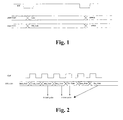
- Figure 1 shows a schematic view of the time pattern of a write enable signal WE for a conventional parallel test protocol;
- Figure 2 shows a schematic view of the time pattern of an LPC protocol signal as relevant to a clock signal;
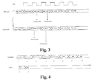
- Figure 3 shows a schematic view of the time pattern of a test cycle according to the inventive method;
- Figure 4 shows a schematic detail view of a protocol particular associated with the testing method of this invention;
- Figure 5 shows a schematic block view of an electronic memory device embodying this invention.
- With reference to the drawing views, in particular to the example of Figure 5, an electronic memory device embodying this invention is generally shown at 1 in schematic form.
- The
device 1 is a non-volatile memory integrated in a semiconductor, e.g. of the flash EEPROM type. It should be understood, however, that the considerations made herein can also be applied to other types of memory devices. - The single prerequisite is that the
device 1 should include aserial interface 2 of the LPC (Low Pin Count) type. - The device conventionally comprises an
array 3 of non-volatile memory cells, as well as of associated row and column decode circuits and memory data read, change and erase circuit portions, not shown because conventional. - The
device 1 comprises a number of circuit blocks interconnected by a set of bus connections, as described here below. - An
address storage block 7, comprising thirty two latch registers and decode logic for the test mode command, is connected to thearray 3 by anADDR address bus 11, which includes a switch b. - The
block 7 generates the test mode signal TM the logic portion incorporated therein. - A DATAL<15:0>
data storage block 8 is connected to thearray 3 by a DBUSdata bus 5. - The
block 8 is loaded with external data through aBUSOUT bus 12, extending from theLPC interface 2. The data are loaded during data cycles into memory locations that are specified by a branch-off 13 of the address bus, which has a switch d connected in and conveys the <15:7> addresses during the address cycles. - A branch-
off 14 of thebus 12 is connected to theblock 7 through a switch c. - Advantageously in this invention, a number of latch registers, in particular a number of
banks 4 of T_latch registers, are provided in thedevice 1 to be accessed via theaddress bus 11. - More particularly, the
bank 4 can be accessed through a branch-off of theaddress bus 11 in which a switch a is connected. - The
bank 4 is closely associated with a T_latch signal generating block 9 that is accessed from thearray 3 over a branch-off of the DBUSbus 5. - The DBUS
bus 5 operates sinchronously to deliver data to the T-latch signal generating block 9, the block 9 being input, additionally to the DBUS signals, the signals from theblock 4 that contain information about the relevant bank number, through a sixteen-bit connection. - In a preferred embodiment, sixteen banks of sixteen T-latches each are available in the
block 4. T_latches are particular registers that, once set for a suitable mode, enable the various paths required to carry out the test, irrespective of the operational state of the device. - The
device 1 also incorporates astate machine 6 that is adapted to generate appropriate enable signals upon receiving the clock pulse CK, as explained hereinafter. - The
state machine 6, additionally to receiving the external clock signal, is also to receive the test mode signal TM, and generates the enable signals of all the protocol steps, further controlling the operation of the switches a, b, c, d. - Of course, the switches provided in the bus connections would be elements adapted to interrupt the parallel inflow of data to each connection in the bus connection bundle.
- Switch a allows to set the
T_latch bank 4. - Switch b interrupts the inflow of addresses to the decode circuit portion of the
array 3. - Switch d allows data to be loaded into the
DATAL block 8. - Switch c allows the external information (LPC<3:0>) present on the
bus 12, as well as on the address or data latches, to be stored in conformity with the communication protocol under consideration. - In essence, the present invention differs from conventional designs in that it contains the following: the
bus connection 13 linking theaddress block 7 to theDATAL block 8, theconnection 15 linking theaddress block 7 to theT_bank signal block 4, and the recognition logic connected in thecontrol block 7 for controlling the test mode TM. - Advantageously in this invention, a test mode access is available for the
device 1, meaning that the test phases usually managed only by the manufacturer can be accessed to fully analyse the device operability. - Accessing in the test mode TM involves the setting of the T_latch bank in a suitable manner.
- The operation of setting the T_latches is unrelated to the device cut, because only the four least-significant addresses and their respective pins are involved. For examples the ADD<3:0> addresses in Figure 5 are adequate to set the
bank 4, with sixteen bits of DBUS<15:0> data being used for setting each of the latches in the respective bank. - Shown in Figure 1, by way of example, is part of a parallel protocol that may be used to set T_latch 1-3, i.e. the third register in the first bank.
- As illustrated by the signal chart of Figure 1, two write enable cycles WE are needed to complete this setting. In the first cycle, a TM-enter code is decoded, and in the second cycle, the relevant T_latch register is driven. Both the addresses and the data are stored upon the rising edge of the signal WE.
- A conventional LPC protocol is further provided, as shown in Figure 2. Figures 1 and 2 illustrate an exemplary write cycle.
- Decoding a command Start is what enables the remainder of the LPC protocol, while the next command Cycle Code serves to discriminate between a read step and a write step.
- There then follow eight cycles, during which the addresses are driven, and two cycles, during which the data to be programmed are driven.
- The next two clock cycles (Tar Code) mark the moment an external host device hands control of the system bus over to the
memory 3. The latter will generate a wait cycle (Sync) and then return the control of the system bus to the external host device in another two Tar Code cycles. - According to this invention, the
device 1 allows entering the test mode TM serially, and then setting the necessary T_latches by using only four input/output pins, in conformity with an LPC serial communication protocol. - Shown in Figure 3 by way of example is a protocol, whereby the T-latch 1-3 can be set as in the previous embodiment, but in a serial manner.
- In this case, setting the T-latch 1-3 involves two protocol cycles, namely:
- a first cycle to drive the codes for entering the test mode TM;
- the second cycle to select the bank and number of the T_latch as shown in Figure 3;
- the eighth address loading cycle contains information about the
T_latch bank 4 of interest; - the sixth and seventh cycles contain information about eight data;
- the two data cycles contain information about the last eight data required.
- Figure 4 shows the codes associated with the second cycle in greater detail.
- The data passed during the sixth and seventh address cycles, and during the two data cycles, will be stored up into a bank of latches, and then synchronously conveyed to the DBUS<15:0>
inner bus 5. - All the T_latch registers in one bank can be set within two full protocol cycles.
- In essence, with the method of this invention, the information required to enter the test mode TM is serially transferred.
- The LPC serial communication protocols are recognized by the memory device on account of the T_latch register bank having been set in advance.
- The device architecture has been optimized to allow the user's test data to be transferred into the T_latch registers in the test mode.
Claims (11)
- An electronic memory device monolithically integrated in a semiconductor and having an LPC (Low Pin Count) serial interface (2), of the type comprising a memory cell array (3) and associated row and column decode circuits; characterized in that it comprises a bank (4) of T_latch registers adapted to be addressed and accessed in a test mode for serially loading specific test data thereinto.
- A device according to Claim 1, characterized in that said registers are operatively linked to an address storage block (7) by an address bus (11,15), on which a switch (a) is provided.
- A device according to Claim 2, characterized in that said address storage block (7) provides a test mode signal (TM) by means of an internal logic unit.
- A device according to Claim 1, characterized in that a block (9), generating signals to said bank (4) of T_latch registers, is accessed from said array (3) by means of a data bus (5).
- A device according to Claim 2, characterized in that it comprises a data storage block (8) connected to said array by a data bus (5) and adapted to receive data over a bus (12) from the LPC interface (2); said data being loaded into memory locations specified by said address storage block (7) through an address bus (13) on which a switch (d) is provided.
- A device according to Claim 3, characterized in that it comprises a state machine (6) operatively linked to a clock signal and to said test mode signal to generate a plurality of enable signals to said switch (a).
- A device according to Claim 4, characterized in that said bank (4) of registers and said signal generating block (9) are connected by a connection of at least sixteen bits.
- A method of testing non-volatile memory devices having at least one LPC (Low Pin Count) serial communication interface and a conventional non-volatile memory cell array (3) and associated read, change, and erase circuits, characterized by:activating a test mode of operation by an address storage block (7) generating a corresponding signal (TM);enabling a bank (4) of T_latch registers in said device to serially receive a predetermined data set; andloading test data into said registers using an LPC serial communication protocol.
- A method according to Claim 8, characterized in that said T_latch registers are set through four input/output pins.
- A method according to Claim 8, characterized in that said registers are set by at least two protocol cycles, namely:a first cycle to drive the test mode entering codes; andthe second cycle to select the bank and number of a T_latch to be used.
- A method according to Claim 8, characterized in that all the T_latch registers belonging to the same bank can be set by means of two protocol cycles.
Priority Applications (2)
| Application Number | Priority Date | Filing Date | Title |
|---|---|---|---|
| EP02425361A EP1367598A1 (en) | 2002-05-31 | 2002-05-31 | Testing method and device for non volatile memories having a LPC (low pin count) communication serial interface |
| US10/447,293 US6785174B2 (en) | 2002-05-31 | 2003-05-28 | Testing method and device for non-volatile memories having a LPC (low pin count) communication serial interface |
Applications Claiming Priority (1)
| Application Number | Priority Date | Filing Date | Title |
|---|---|---|---|
| EP02425361A EP1367598A1 (en) | 2002-05-31 | 2002-05-31 | Testing method and device for non volatile memories having a LPC (low pin count) communication serial interface |
Publications (1)
| Publication Number | Publication Date |
|---|---|
| EP1367598A1 true EP1367598A1 (en) | 2003-12-03 |
Family
ID=29414878
Family Applications (1)
| Application Number | Title | Priority Date | Filing Date |
|---|---|---|---|
| EP02425361A Ceased EP1367598A1 (en) | 2002-05-31 | 2002-05-31 | Testing method and device for non volatile memories having a LPC (low pin count) communication serial interface |
Country Status (2)
| Country | Link |
|---|---|
| US (1) | US6785174B2 (en) |
| EP (1) | EP1367598A1 (en) |
Families Citing this family (7)
| Publication number | Priority date | Publication date | Assignee | Title |
|---|---|---|---|---|
| US8412853B2 (en) * | 2004-10-25 | 2013-04-02 | Texas Instruments Incorporated | Two pin serial bus communication interface |
| ITVA20030022A1 (en) * | 2003-07-07 | 2005-01-08 | St Microelectronics Srl | METHOD OF GENERATION OF A SIGNAL OF ENABLING IN A MULTI-PROTOCOL MEMORY AND RELATIVE MEMORY DEVICE. |
| TWI270803B (en) * | 2004-10-08 | 2007-01-11 | Via Tech Inc | Adapter for memory simulator |
| ITMI20042072A1 (en) * | 2004-10-29 | 2005-01-29 | St Microelectronics Srl | FLSH MEMORY DEVICE EQUIPPED WITH LOW PIN COUNT COMMUNICATION INTERFACE |
| US7882405B2 (en) * | 2007-02-16 | 2011-02-01 | Atmel Corporation | Embedded architecture with serial interface for testing flash memories |
| US7769943B2 (en) * | 2007-04-04 | 2010-08-03 | Atmel Corporation | Flexible, low cost apparatus and method to introduce and check algorithm modifications in a non-volatile memory |
| US8844023B2 (en) * | 2008-12-02 | 2014-09-23 | Micron Technology, Inc. | Password protected built-in test mode for memories |
Citations (3)
| Publication number | Priority date | Publication date | Assignee | Title |
|---|---|---|---|---|
| EP0651261A2 (en) * | 1993-11-02 | 1995-05-03 | International Business Machines Corporation | System and method for testing a circuit network having elements testable by different boundary scan standards |
| US5687179A (en) * | 1990-03-30 | 1997-11-11 | Texas Instruments Incorporated | Serial data input/output method and apparatus |
| EP1018746A1 (en) * | 1999-01-08 | 2000-07-12 | SUMITOMO WIRING SYSTEMS, Ltd. | Method for writing data into non-volatile memory in vehicle electronic unit |
Family Cites Families (2)
| Publication number | Priority date | Publication date | Assignee | Title |
|---|---|---|---|---|
| US5596734A (en) * | 1993-12-17 | 1997-01-21 | Intel Corporation | Method and apparatus for programming embedded memories of a variety of integrated circuits using the IEEE test access port |
| JP2001084787A (en) * | 1999-09-09 | 2001-03-30 | Oki Electric Ind Co Ltd | Rewriting circuit for nonvolatile storage device, rewriting method for nonvolatile storage device, and scan register |
-
2002
- 2002-05-31 EP EP02425361A patent/EP1367598A1/en not_active Ceased
-
2003
- 2003-05-28 US US10/447,293 patent/US6785174B2/en not_active Expired - Lifetime
Patent Citations (3)
| Publication number | Priority date | Publication date | Assignee | Title |
|---|---|---|---|---|
| US5687179A (en) * | 1990-03-30 | 1997-11-11 | Texas Instruments Incorporated | Serial data input/output method and apparatus |
| EP0651261A2 (en) * | 1993-11-02 | 1995-05-03 | International Business Machines Corporation | System and method for testing a circuit network having elements testable by different boundary scan standards |
| EP1018746A1 (en) * | 1999-01-08 | 2000-07-12 | SUMITOMO WIRING SYSTEMS, Ltd. | Method for writing data into non-volatile memory in vehicle electronic unit |
Non-Patent Citations (1)
| Title |
|---|
| NADEAU-DOSTIE B ET AL: "SERIAL INTERFACING FOR EMBEDDED-MEMORY TESTING", IEEE DESIGN & TEST OF COMPUTERS, IEEE COMPUTERS SOCIETY. LOS ALAMITOS, US, vol. 7, no. 2, April 1990 (1990-04-01), pages 52 - 63, XP000159643, ISSN: 0740-7475 * |
Also Published As
| Publication number | Publication date |
|---|---|
| US6785174B2 (en) | 2004-08-31 |
| US20040071028A1 (en) | 2004-04-15 |
Similar Documents
| Publication | Publication Date | Title |
|---|---|---|
| US6324096B1 (en) | Interface circuit and method for writing data into a non-volatile memory, and scan register | |
| US5966723A (en) | Serial programming mode for non-volatile memory | |
| US6829673B2 (en) | Latched address multi-chunk write to EEPROM | |
| US5949987A (en) | Efficient in-system programming structure and method for non-volatile programmable logic devices | |
| US20080109594A1 (en) | Non-volatile memory device controlled by a micro-controller | |
| EP0967723A2 (en) | Programmable pin designation for semiconductor devices | |
| US20040059906A1 (en) | System and method for booting by use of a flash memory | |
| WO1994008399A1 (en) | Arrangement for parallel programming of in-system programmable ic logic devices | |
| CN100442395C (en) | Integrated circuit with self-test device and related test method | |
| US7538577B2 (en) | System and method for configuring a field programmable gate array | |
| US6785174B2 (en) | Testing method and device for non-volatile memories having a LPC (low pin count) communication serial interface | |
| US6894914B2 (en) | Nonvolatile memory device with parallel and serial functioning mode and selectable communication protocol | |
| US8423701B2 (en) | Flash memory device with a low pin count (LPC) communication interface | |
| US7308623B2 (en) | Integrated circuit and method for testing memory on the integrated circuit | |
| WO1999030219A9 (en) | Method and apparatus for in-system programming | |
| US20070250740A1 (en) | System and method for conducting BIST operations | |
| US20060036803A1 (en) | Non-volatile memory device controlled by a micro-controller | |
| US6590414B2 (en) | Circuit architecture for performing a trimming operation on integrated circuits | |
| JPH07192481A (en) | Semiconductor memory device | |
| US6975559B2 (en) | Device and method for reading non-volatile memories having at least one pseudo-parallel communication interface | |
| US5566109A (en) | EEPROM, write control method for EEPROM, and IC card | |
| US20040148499A1 (en) | Method and apparatus for programming revision identification numbers | |
| US7130787B1 (en) | Functional replicator of a specific integrated circuit and its use as an emulation device | |
| US7231487B2 (en) | Automatic decoding method for mapping and selecting a non-volatile memory device having a LPC serial communication interface in the available addressing area on motherboards | |
| US7209252B2 (en) | Memory module, printer assembly, and method for storing printer code |
Legal Events
| Date | Code | Title | Description |
|---|---|---|---|
| PUAI | Public reference made under article 153(3) epc to a published international application that has entered the european phase |
Free format text: ORIGINAL CODE: 0009012 |
|
| AK | Designated contracting states |
Kind code of ref document: A1 Designated state(s): AT BE CH CY DE DK ES FI FR GB GR IE IT LI LU MC NL PT SE TR |
|
| AX | Request for extension of the european patent |
Extension state: AL LT LV MK RO SI |
|
| 17P | Request for examination filed |
Effective date: 20040421 |
|
| AKX | Designation fees paid |
Designated state(s): DE FR GB IT |
|
| 17Q | First examination report despatched |
Effective date: 20050303 |
|
| 17Q | First examination report despatched |
Effective date: 20050303 |
|
| STAA | Information on the status of an ep patent application or granted ep patent |
Free format text: STATUS: THE APPLICATION HAS BEEN REFUSED |
|
| 18R | Application refused |
Effective date: 20090617 |