EP1365506B1 - Up-converter for radio systems - Google Patents
Up-converter for radio systems Download PDFInfo
- Publication number
- EP1365506B1 EP1365506B1 EP02425322A EP02425322A EP1365506B1 EP 1365506 B1 EP1365506 B1 EP 1365506B1 EP 02425322 A EP02425322 A EP 02425322A EP 02425322 A EP02425322 A EP 02425322A EP 1365506 B1 EP1365506 B1 EP 1365506B1
- Authority
- EP
- European Patent Office
- Prior art keywords
- signal
- amplifier
- converted
- chain
- gain
- Prior art date
- Legal status (The legal status is an assumption and is not a legal conclusion. Google has not performed a legal analysis and makes no representation as to the accuracy of the status listed.)
- Expired - Lifetime
Links
- 238000010586 diagram Methods 0.000 description 7
- 230000006835 compression Effects 0.000 description 3
- 238000007906 compression Methods 0.000 description 3
- 238000000034 method Methods 0.000 description 3
- 230000015556 catabolic process Effects 0.000 description 2
- 238000006731 degradation reaction Methods 0.000 description 2
- 238000004519 manufacturing process Methods 0.000 description 2
- 238000001228 spectrum Methods 0.000 description 2
- 239000004593 Epoxy Substances 0.000 description 1
- 241001125929 Trisopterus luscus Species 0.000 description 1
- 230000003044 adaptive effect Effects 0.000 description 1
- 230000002411 adverse Effects 0.000 description 1
- 230000003321 amplification Effects 0.000 description 1
- 230000005540 biological transmission Effects 0.000 description 1
- 239000000919 ceramic Substances 0.000 description 1
- 230000001010 compromised effect Effects 0.000 description 1
- 238000010276 construction Methods 0.000 description 1
- 230000003247 decreasing effect Effects 0.000 description 1
- 238000013461 design Methods 0.000 description 1
- 238000011161 development Methods 0.000 description 1
- 230000018109 developmental process Effects 0.000 description 1
- 238000005516 engineering process Methods 0.000 description 1
- 230000001747 exhibiting effect Effects 0.000 description 1
- 238000003780 insertion Methods 0.000 description 1
- 230000037431 insertion Effects 0.000 description 1
- 238000003199 nucleic acid amplification method Methods 0.000 description 1
- 239000000758 substrate Substances 0.000 description 1
- 230000001360 synchronised effect Effects 0.000 description 1
- 238000012360 testing method Methods 0.000 description 1
- 238000009966 trimming Methods 0.000 description 1
Images

Classifications
-
- H—ELECTRICITY
- H03—ELECTRONIC CIRCUITRY
- H03G—CONTROL OF AMPLIFICATION
- H03G3/00—Gain control in amplifiers or frequency changers
- H03G3/20—Automatic control
- H03G3/30—Automatic control in amplifiers having semiconductor devices
- H03G3/3036—Automatic control in amplifiers having semiconductor devices in high-frequency amplifiers or in frequency-changers
Definitions
- the present invention refers to up-converters for radio systems and was developed by paying specific attention to the ever-increasing need for high performance up-converters for mmw (millimeter wave) radio systems.
- the present invention relates to an up-converter circuit according to the preamble of claim 1, which is known, e.g. from US 2001/0053676
- microwave transmitters In order to meet those requirements, microwave transmitters, and especially those operating in the mmw frequency bands (i.e. in frequency ranges leading to very critical operating conditions for circuitry) must exhibit good performance in terms of linearity (IP3 - P 1dB - IMR3), output power dynamic range, dc power consumption and output noise power density.
- linearity IP3 - P 1dB - IMR3
- output power dynamic range i.e. in frequency ranges leading to very critical operating conditions for circuitry
- the up-converter circuit of this kind are arranged in such way to include:
- the object of the present invention is to overcame some of the intrinsic drawbacks of those prior art arrangements, i.e. to provide an up-converter adapted for operation in the mmw frequency bands ensuring a good performance level while also exhibiting lower production cost (including assembly and tuning).
- the claimed up converter permits degradation to be easily controlled having each amplifier stage of said plurality a respective, selectively controllable gain value, and at least one gain control module for varying said given gain value of said RF amplifier chain by uniformly varying the respective gains of said amplifier stages.
- the present architecture does not require any additional variable attenuator device; in this way it is not necessary to insert further amplification stage (to compensate variable attenuator insertion loss), and dc power consumption is optimised according to the output power level setting.
- an up-converter adapted for operating e.g. in the 38 and 41 GHz frequency bands is designated 1 as a whole.
- the input stage of up-converter 1 is essentially comprised of a low noise amplifier (LNA) stage operating in the intermediate frequency (IF) range.
- the IF stage in question includes an IF pre-amplifier 10 having an input line 10a for receiving an IF input signal to be frequency up-converted.
- Cascaded with pre-amplifier 10 is preferably an IF automatic gain control (AGC) block 11 having an input control line receiving a temperature control signal generated by a comparator 12.
- AGC automatic gain control
- a first input of comparator 12 is connected to a temperature control circuit 13 fed with a temperature signal generated by a temperature sensor 14.
- the other input of comparator 12 is connected to an IF gain setting unit 15 essentially comprised of a potentiometer.
- the output signal from the IF section comprised of pre-amplifier 10 and gain control block 11 is fed to mixer stage 16 which is preferably comprised of a LO-Image reject mixer fed with the signal generated by a local oscillator 17.
- an RF signal is generated which substantially corresponds to the IF signal input on line 10a up-converted by a frequency value corresponding to the value of the frequency of the local signal generated by oscillator 17.
- Reference numerals 18a, 18b and 18c designate a plurality of amplifier stages making up an RF amplifier chain adapted to generate on an output line 19 an RF output signal adapted to be fed e.g. to an antenna (not shown).
- the number of amplifier stages comprising the RF amplifier chain may be different from three. Essentially, depending on the expected application, the number of such RF amplifier stages is selected as a judicious compromise between the overall gain value to be achieved and circuit complexity.
- Each of amplifier stages 18a, 18b, 18c has associated therewith a biasing network 180a, 180b, 180c.
- Reference 20 designates a radio frequency detector of a known type associated with output line 19 to detect the power level at the output of the RF amplifier chain including amplifier stages 18a, 18b and 18c.
- the output signal from power detector 20 is fed to an automatic gain control (AGC) circuit 21.
- AGC automatic gain control
- AGC circuit 21 is adapted to selectively vary the gain figure of the RF amplifier chain comprising stages 18a, 18b and 18c by acting or biasing networks 180a, 180b, 180c according to principles which will be described in greater detail in the following.
- circuit 21 is controlled through a line 21 a by a RF gain setting unit 22 of a known type.
- the automatic gain control signal generated by circuit 21 is fed back over a line 23 towards the stages 18a, 18b, and 18c of the RF amplifier chain.
- line 23 is connected with one or more biasing networks 180a, 180b and 180c to selectively control the gain values of amplifier stages 18a, 18b and 18c as better described in the following.
- Reference 24 designates a switch which permits the automatic gain control (AGC) feedback loop from circuit 21 represented by line 23 to be selectively interrupted in order to connect line 23 to a fixed voltage value (e.g. -5 volt) to permit manual gain control (MGC) during preliminary adjustment and trimming procedures and/or during testing.
- AGC automatic gain control
- block 11 and the circuitry associated therewith, comprised of elements 12 to 15, is intended to control gain of the IF section (10, 11) of the up-converter in order to compensate temperature drift phenomena.
- the AGC function proper is performed in the RF section by properly varying (via networks 180a, 180b and 180c) the operating conditions of amplifier stages 18a, 18b and 18c.
- the arrangement shown in figure 1 does not involve any additional attenuator circuit in the RF section which represents an appreciable advantage over prior art arrangements including such circuits by taking into account that e.g. pin diode attenuators, while providing good linearity, are not easy to implement by resorting to MMIC devices in the millimeter wave operating range.
- a high level up-converter mixer 16 is used. In that way the input noise figure is improved by using a LNA IF stage.
- the overall gain of the amplifying chain comprised of stages 18a, 18b and 18c is selectively varied by correspondingly varying - in a uniform manner - the gain of each and every stage included therein.
- variable bias current sources 180a, 180b, 180c preferably having the general structure shown in figure 2.
- the amplifying chain is thus dimensioned according to linearity criteria while making sure that the driver stages do not lead to an undesired compression of the signal in the following stages.
- a current source as shown in figure 2 is preferably provided for each of the amplifier stages 18a, 18b and 18c of the RF amplifier chain shown in figure 1. Arrangements wherein one such current source is provided for driving two or more of the amplifier stages 18a, 18b, 18c are also within the scope of the present invention.
- the block diagram of figure 2 shows the typical arrangement of a current source adapted to be controlled via a control line: this is designated 23 for the sake of consistency with the block diagram of figure 1.
- both I d and V d may be controlled.
- the emitter-collector line of transistor 25 is connected between a power feed line Vcc at and a (preferably negative) reference value - Vcc.
- the emitter and collector of transistor 24 have associated respective resistor designated 26 and 27, respectively.
- Corresponding signals for driving the drain and gate electrodes of the FET amplifier(s) included in stages 18a, 18b, and 18c can thus be drawn from respective bias control lines at the emitter (line 26a) and the collector (line 27a) of transistor 25, respectively.
- the base of transistor 25 is connected to the intermediate point of a voltage divider including two resistors 28 and 29 connected in series between the power feed voltage Vcc and the voltage control point connected to feedback line 23.
- the diagram of figure 4 shows the output power (Pout - mW) versus input power (Pin - mW) of a FET amplifier stage for different values of drain current for drain current values (I d ) corresponding to 10 mA (I), 30 mA (II), 50 mA (III), 70 mA (IV) and 90 mA (V), respectively.
- the arrangement of the invention overcomes the intrinsic drawbacks of those prior art arrangements aiming at automatically controlling gain by keeping the compression power constant as gain is varied.
- the arrangement disclosed permits degradation to be easily controlled since, as I d varies, the ratio between the "useful" signal and the intermodulation products is kept constant.
- the gain control technique just described is particularly adapted to be carried out on a RF amplifier chain.
- the gain of the whole RF amplifier chain (stages 18a, 18b, and 18c) is varied by simultaneously and uniformly varying the gain values of each and every stage in the chain.
- output power may be optimised versus dc power consumption. This is due to a lower current being needed for low output power levels.
- Such a feature is particularly useful in systems using power control arrangements of the ATPC (Automatic Transmitter Power Control) or RTPC (Remote Transmitter Power Control) type during normal operation, e.g. at low power levels because of the lower dc power consumption. Operation temperature is also decreased, thus improving the transmitter MTBF.
- ATPC Automatic Transmitter Power Control
- RTPC Remote Transmitter Power Control
- up-converter 11 is implemented by resorting to microstrip transmission line technology using MMIC devices and ceramic substrate hybrids.
- Such an assembly is adapted for fully automated production using epoxy attach techniques. No manual tuning of converter 1 is required and output power calibration may be carried out by means of a fully automated software-controlled routine.
- the invention thus provides an improved up-converter arrangement adapted for operating in the mm-wave frequency bands for radio applications.
- the main features of such an arrangement are high linearity and dynamic range, adaptive dc power consumption and low noise figure.
Landscapes
- Superheterodyne Receivers (AREA)
- Amplifiers (AREA)
- Transmitters (AREA)
- Control Of Amplification And Gain Control (AREA)
Abstract
Description
- The present invention refers to up-converters for radio systems and was developed by paying specific attention to the ever-increasing need for high performance up-converters for mmw (millimeter wave) radio systems.
- More specifically the present invention relates to an up-converter circuit according to the preamble of
claim 1, which is known, e.g. fromUS 2001/0053676 - Recent developments in radio network standards (ETSI, FCCI, ...), particularly in respect of SDH (Synchronous Digital Hierarchy), BWA (Broadband Wireless Access) and PtMP (Point to MultiPoint) systems impose increasingly severe requirements in terms of output power spectrum masks. These include strict requirements in term of transmitted spectrum mask constrains and noise output power during switch off in burst mode operation.
- In order to meet those requirements, microwave transmitters, and especially those operating in the mmw frequency bands (i.e. in frequency ranges leading to very critical operating conditions for circuitry) must exhibit good performance in terms of linearity (IP3 - P1dB - IMR3), output power dynamic range, dc power consumption and output noise power density.
- The up-converter circuit of this kind are arranged in such way to include:
- an input stage for producing an IF signal to be frequency up-converted,
- a local oscillator for generating a local oscillator signal,
- a mixer stage fed with said IF signal and said local oscillator signal for generating an up-converted RF signal by mixing said IF signal and said local oscillator signal,
- a RF amplifier chain fed with said up-converted RF signal for amplifying said up-converted RF signal by a given gain value, wherein said amplifier chain includes a plurality of linear attenuation stages and means aiming at automatically controlling gain by keeping the compression power constant as output power level is varied.
- The object of the present invention is to overcame some of the intrinsic drawbacks of those prior art arrangements, i.e. to provide an up-converter adapted for operation in the mmw frequency bands ensuring a good performance level while also exhibiting lower production cost (including assembly and tuning).
- According to the present invention that object is achieved by means of an up-converter having the features called for in
claim 1. - The claimed up converter permits degradation to be easily controlled having each amplifier stage of said plurality a respective, selectively controllable gain value, and at least one gain control module for varying said given gain value of said RF amplifier chain by uniformly varying the respective gains of said amplifier stages. The present architecture, does not require any additional variable attenuator device; in this way it is not necessary to insert further amplification stage (to compensate variable attenuator insertion loss), and dc power consumption is optimised according to the output power level setting.
- The invention will now be described, by way of example only, with reference to the annexed figures of drawings, wherein:
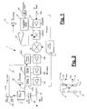
- Figure 1 is a block diagram of an up-converter according to the invention,
- Figure 2 is a block diagram of a bias source adapted for use in the up-converter of the invention,
- Figure 3 is a diagram showing the gain v. drain current relationship in a FET amplifier stage adapted for use in the invention, and
- Figure 4 is a diagram showing the output power v. input power relationship in a converter according to the invention.
- In figure 1 an up-converter adapted for operating e.g. in the 38 and 41 GHz frequency bands is designated 1 as a whole.
- Of course, the indicated frequency bands are for exemplary purposes only and must in no way be construed as limiting the scope of the invention.
- The input stage of up-
converter 1 is essentially comprised of a low noise amplifier (LNA) stage operating in the intermediate frequency (IF) range. The IF stage in question includes an IF pre-amplifier 10 having aninput line 10a for receiving an IF input signal to be frequency up-converted. Cascaded with pre-amplifier 10 is preferably an IF automatic gain control (AGC)block 11 having an input control line receiving a temperature control signal generated by acomparator 12. - A first input of
comparator 12 is connected to atemperature control circuit 13 fed with a temperature signal generated by atemperature sensor 14. The other input ofcomparator 12 is connected to an IFgain setting unit 15 essentially comprised of a potentiometer. - The arrangement made up of
blocks 11 to 15 is conventional in the art and, as such, does not require to be described in greater detail here. - The output signal from the IF section comprised of pre-amplifier 10 and
gain control block 11 is fed tomixer stage 16 which is preferably comprised of a LO-Image reject mixer fed with the signal generated by alocal oscillator 17. - As a result of mixing in
mixer 16, an RF signal is generated which substantially corresponds to the IF signal input online 10a up-converted by a frequency value corresponding to the value of the frequency of the local signal generated byoscillator 17. -
Reference numerals output line 19 an RF output signal adapted to be fed e.g. to an antenna (not shown). - Even though three
amplifier stages - Each of
amplifier stages biasing network -
Reference 20 designates a radio frequency detector of a known type associated withoutput line 19 to detect the power level at the output of the RF amplifier chain includingamplifier stages power detector 20 is fed to an automatic gain control (AGC)circuit 21. -
AGC circuit 21 is adapted to selectively vary the gain figure of the RF amplifierchain comprising stages biasing networks - Specifically,
circuit 21 is controlled through aline 21 a by a RFgain setting unit 22 of a known type. - The automatic gain control signal generated by
circuit 21 is fed back over aline 23 towards thestages - Specifically,
line 23 is connected with one ormore biasing networks amplifier stages -
Reference 24 designates a switch which permits the automatic gain control (AGC) feedback loop fromcircuit 21 represented byline 23 to be selectively interrupted in order to connectline 23 to a fixed voltage value (e.g. -5 volt) to permit manual gain control (MGC) during preliminary adjustment and trimming procedures and/or during testing. - It will be appreciated that
block 11 and the circuitry associated therewith, comprised ofelements 12 to 15, is intended to control gain of the IF section (10, 11) of the up-converter in order to compensate temperature drift phenomena. - Conversely, the AGC function proper is performed in the RF section by properly varying (via
networks amplifier stages - The arrangement shown in figure 1 does not involve any additional attenuator circuit in the RF section which represents an appreciable advantage over prior art arrangements including such circuits by taking into account that e.g. pin diode attenuators, while providing good linearity, are not easy to implement by resorting to MMIC devices in the millimeter wave operating range.
- Conversely, in the arrangement shown, to reduce gain at the RF level a high level up-
converter mixer 16 is used. In that way the input noise figure is improved by using a LNA IF stage. - In order to provide the desired output power dynamic range while preserving noise figure and IMR3 (linearity) performance, the overall gain of the amplifying chain comprised of
stages - This is preferably done by correspondingly varying the gain value for each stage in the chain in a uniform way by using variable bias
current sources - In order to properly operate the millimeter wave amplifying chain comprised of
amplifier stages - In a preferred embodiment of the invention, a current source as shown in figure 2 is preferably provided for each of the
amplifier stages amplifier stages - In order to understand operation of such a current source, reference may be had to figure 3 of the drawings showing the relationship between the drain current Id (mA - horizontal scale) and the gain (dB - vertical scale) in a typical FET amplifier stage.
- The block diagram of figure 2 shows the typical arrangement of a current source adapted to be controlled via a control line: this is designated 23 for the sake of consistency with the block diagram of figure 1.
- Assuming optimal matching conditions with the load and that the saturation region of a FET amplifier is ideal, the maximum output power Pmax (with no harmonic distortion) may be expressed as:

where Id and Vd correspond to the drain current intensity and the drain voltage, respectively. - As a consequence of this, in order to vary the gain of the
stages - This can be obtained by means of the arrangement of figure 2 including a
BJT transistor 25. - The emitter-collector line of
transistor 25 is connected between a power feed line Vcc at and a (preferably negative) reference value - Vcc. - The emitter and collector of
transistor 24 have associated respective resistor designated 26 and 27, respectively. Corresponding signals for driving the drain and gate electrodes of the FET amplifier(s) included instages line 26a) and the collector (line 27a) oftransistor 25, respectively. - The base of
transistor 25 is connected to the intermediate point of a voltage divider including tworesistors feedback line 23. - The diagram of figure 4 shows the output power (Pout - mW) versus input power (Pin - mW) of a FET amplifier stage for different values of drain current for drain current values (Id) corresponding to 10 mA (I), 30 mA (II), 50 mA (III), 70 mA (IV) and 90 mA (V), respectively.
- It will be appreciated that the arrangement of the invention overcomes the intrinsic drawbacks of those prior art arrangements aiming at automatically controlling gain by keeping the compression power constant as gain is varied. The arrangement disclosed permits degradation to be easily controlled since, as Id varies, the ratio between the "useful" signal and the intermodulation products is kept constant.
- The gain control technique just described is particularly adapted to be carried out on a RF amplifier chain.
- The choice of the component on which gain control is to be performed is in fact critical as it affects both the noise figure and the level of intermodulation products.
- In a chain including n stages, if gain control is performed at one of the input stages of the chain, the noise figure is adversely affected. Conversely, if control is performed at one of the last stages in the chain, linearity is compromised. The arrangement of the invention provides for those parameters being controlled concurrently, in order to preserve the overall performance of the system while ensuring a reasonably high gain dynamics.
- In the arrangement of the invention, in order to provide output power dynamic range while safeguarding performance in terms of the noise figure and linearity (IMR3) the gain of the whole RF amplifier chain (
stages - In the case of FET amplifier stages, this is done preferably by controlling the values of the drain current Id of each stage. In order to operate properly, the whole chain is designed according to linearity criteria, ensuring that drivers should not compress subsequent stages.
- In the arrangement of the invention, output power may be optimised versus dc power consumption. This is due to a lower current being needed for low output power levels.
- Such a feature is particularly useful in systems using power control arrangements of the ATPC (Automatic Transmitter Power Control) or RTPC (Remote Transmitter Power Control) type during normal operation, e.g. at low power levels because of the lower dc power consumption. Operation temperature is also decreased, thus improving the transmitter MTBF.
- In the presently preferred embodiment up-
converter 11 is implemented by resorting to microstrip transmission line technology using MMIC devices and ceramic substrate hybrids. - Such an assembly is adapted for fully automated production using epoxy attach techniques. No manual tuning of
converter 1 is required and output power calibration may be carried out by means of a fully automated software-controlled routine. - A summary of the most significant performance parameters of an exemplary embodiment of an up-converter according to the invention is provided in Table 1 that follows.
Frequency range 37÷39.5 GHz 40.5÷43.5 GHz Output power dynamic range 1÷21 dBm IMR3 With reference to single channel level >= 40 dBc @ any Pout NF at input port ≤ 15dB @ Pmax ≤ 25 dB @ Pmin Dc power consumption ≤ 12 W @ Pmax ≤ 7 W @ Pmin - The invention thus provides an improved up-converter arrangement adapted for operating in the mm-wave frequency bands for radio applications. The main features of such an arrangement are high linearity and dynamic range, adaptive dc power consumption and low noise figure.
- Of course, without prejudice to the principle of the invention, the details of construction and the embodiments may widely vary with respect to what has been described and illustrated purely by way of example, without departing from the scope of the present invention.
The data sheet Agilent HMMC-1002 DC-50 Ghz Attenuator, printed on February 19, 2001 shows a Voltage Variable Attenuators (VVA) implemented in mmw IC form. They provide good dynamic range but suffer from linearity problems since Fet junctions (a no linear element) is used as variable resistors.
Claims (5)
- An up-converter circuit (1) comprising:- an input stage (10, 11) for producing an IF signal to be frequency up-converted,- a local oscillator (17) for generating a local oscillator signal,- a mixer stage (16) fed with said IF signal and said local oscillator signal for generating an up-converted RF signal by mixing said IF signal and said local oscillator signal,- a RF amplifier chain (18a, 18b, 18c) fed with said up-converted RF signal for amplifying said up-converted RF signal by a given gain value,characterised in that said amplifier chain includes:a) a plurality of amplifier stages (18a, 18b, 18c), wherein each amplifier stage of said plurality have a respective, selectively controllable gain value,b) at least one gain control module (180a, 180b, 180c) is provided for varying said given gain value of said RF amplifier chain by uniformly varying the respective gains of said amplifier stages (18a, 18b, 18c) of said RF amplifier chain andsaid at least one gain control module (180a, 180b, 180c) has associated therewith a RF power detector (20) for sensing the power of said up-converted RF signal as amplified by said given gain value by said RF amplifier chain (18a, 18b, 18c) wherein said respective gains of the amplifier stages (18a, 18b, 18c) of said RF amplifier chain are selectively varied as a function of said power of said up-converted and amplified RF signal.
- The circuit of claim 1 , characterised in that the amplifier stages (18a, 18b, 18c) of said RF amplifier chain are FET amplifier stages, wherein said respective gains of said amplifier stages (18a, 18b, 18c) are varied by varying at least one the drain current (Id) and the drain-source voltage (Vds) of the FET amplifier stage.
- The circuit of claim 2, characterised in that said at least one gain control module (180a, 180b, 180c) includes:- a gain control input port (23) adapted to be brought to a given gain control voltage,- a transistor (25) having base, emitter and collector ports, and- a voltage divider (28, 29) sensitive to said given voltage at said gain control input port (23), said voltage divider having a tap point connected to the base port of said transistor (25), wherein said emitter and collector ports of said transistor (25) are connected to the drain and the gate ports, respectively, of at least one of said FET amplifier stages in said RF amplifier chain (18a, 18b, 18c).
- The circuit of any of the previous claims, characterised in that said input stage (10, 11) includes at least one variable gain block (11) as well as temperature-sensitive control circuitry (12 to 15) for selectively varying the gain of said at least one block (11) as a function of temperature.
- The circuit of any of the previous claims, characterised in that said RF amplifier chain (18a, 18b, 18c) is configured to operate in the tens of GHz range preferably in the 40 GHz range.
Priority Applications (3)
| Application Number | Priority Date | Filing Date | Title |
|---|---|---|---|
| EP02425322A EP1365506B1 (en) | 2002-05-22 | 2002-05-22 | Up-converter for radio systems |
| DE60223501T DE60223501T2 (en) | 2002-05-22 | 2002-05-22 | Up-frequency converter for radio systems |
| AT02425322T ATE378731T1 (en) | 2002-05-22 | 2002-05-22 | UP FREQUENCY CONVERTER FOR RADIO SYSTEMS |
Applications Claiming Priority (1)
| Application Number | Priority Date | Filing Date | Title |
|---|---|---|---|
| EP02425322A EP1365506B1 (en) | 2002-05-22 | 2002-05-22 | Up-converter for radio systems |
Publications (2)
| Publication Number | Publication Date |
|---|---|
| EP1365506A1 EP1365506A1 (en) | 2003-11-26 |
| EP1365506B1 true EP1365506B1 (en) | 2007-11-14 |
Family
ID=29286266
Family Applications (1)
| Application Number | Title | Priority Date | Filing Date |
|---|---|---|---|
| EP02425322A Expired - Lifetime EP1365506B1 (en) | 2002-05-22 | 2002-05-22 | Up-converter for radio systems |
Country Status (3)
| Country | Link |
|---|---|
| EP (1) | EP1365506B1 (en) |
| AT (1) | ATE378731T1 (en) |
| DE (1) | DE60223501T2 (en) |
Families Citing this family (1)
| Publication number | Priority date | Publication date | Assignee | Title |
|---|---|---|---|---|
| CN1331310C (en) * | 2005-04-11 | 2007-08-08 | 南京理工大学 | High power millimeter wave upper frequency converter power amplification assembly based on three branch combining network |
Family Cites Families (4)
| Publication number | Priority date | Publication date | Assignee | Title |
|---|---|---|---|---|
| US5493255A (en) * | 1995-03-21 | 1996-02-20 | Nokia Mobile Phones Ltd. | Bias control circuit for an RF power amplifier |
| US5774017A (en) * | 1996-06-03 | 1998-06-30 | Anadigics, Inc. | Multiple-band amplifier |
| US6175279B1 (en) * | 1997-12-09 | 2001-01-16 | Qualcomm Incorporated | Amplifier with adjustable bias current |
| US6104246A (en) * | 1999-05-25 | 2000-08-15 | International Business Machines Corporation | Variable gain RF amplifier with switchable bias injection and feedback |
-
2002
- 2002-05-22 AT AT02425322T patent/ATE378731T1/en not_active IP Right Cessation
- 2002-05-22 DE DE60223501T patent/DE60223501T2/en not_active Expired - Lifetime
- 2002-05-22 EP EP02425322A patent/EP1365506B1/en not_active Expired - Lifetime
Also Published As
| Publication number | Publication date |
|---|---|
| DE60223501T2 (en) | 2008-04-30 |
| DE60223501D1 (en) | 2007-12-27 |
| ATE378731T1 (en) | 2007-11-15 |
| EP1365506A1 (en) | 2003-11-26 |
Similar Documents
| Publication | Publication Date | Title |
|---|---|---|
| CA2109810C (en) | Power control circuitry for achieving wide dynamic range in a transmitter | |
| US5915213A (en) | Transmitter apparatus with linearizing circuit to compensate for distortion in power amplifier | |
| EP1526651B1 (en) | Additional regulation of the reference signal of the automatic power control in a mobile terminal | |
| US5182527A (en) | Power amplifying apparatus for wireless transmitter | |
| US5126688A (en) | Power amplifying apparatus for wireless transmitter | |
| EP0472330B1 (en) | Transmission output control circuit | |
| KR100312367B1 (en) | Mobile communication device and method | |
| US7656227B1 (en) | Techniques to control amplifier gain over process, voltage, and/or temperature (PVT) variations | |
| EP0818879B1 (en) | Amplifier circuit and multistage amplifier circuit | |
| CN102647155A (en) | Variable gain amplifier | |
| US6091942A (en) | Self gain aligning circuit and method | |
| CN100579103C (en) | An automatic power control device and method for a QAM transmitter unit of a wireless communication device | |
| US8055223B2 (en) | Radio receiver | |
| KR20010090475A (en) | Transmitter circuit with frequency self-optimization | |
| EP1365506A1 (en) | Up-converter for radio systems | |
| KR20030019311A (en) | Power booster method and apparatus for improving the performance of radio frequency linear power amplifiers | |
| EP1478104A1 (en) | Variable transmission power steps | |
| GB2359680A (en) | A linear transmitter with stabilization of loop gain under load variation | |
| US20070080746A1 (en) | Glitch-free controllable rf power amplifier | |
| US6647072B1 (en) | Transmitting circuit improving SN ratio in low output power and CN ratio in low to intermediate output power | |
| CN214380827U (en) | Radio frequency automatic control circuit with gain adjustment function | |
| US6091299A (en) | Method and apparatus for achieving linearized response of PIN diode attenuators | |
| US6518843B1 (en) | Variable gain type amplifier | |
| KR100312216B1 (en) | Tx power amplifier | |
| JP2002344333A (en) | High frequency circuit and high frequency communication device using the same |
Legal Events
| Date | Code | Title | Description |
|---|---|---|---|
| PUAI | Public reference made under article 153(3) epc to a published international application that has entered the european phase |
Free format text: ORIGINAL CODE: 0009012 |
|
| AK | Designated contracting states |
Kind code of ref document: A1 Designated state(s): AT BE CH CY DE DK ES FI FR GB GR IE IT LI LU MC NL PT SE TR |
|
| AX | Request for extension of the european patent |
Extension state: AL LT LV MK RO SI |
|
| 17P | Request for examination filed |
Effective date: 20040419 |
|
| RAP1 | Party data changed (applicant data changed or rights of an application transferred) |
Owner name: SIEMENS MOBILE COMMUNICATIONS S.P.A. |
|
| AKX | Designation fees paid |
Designated state(s): AT BE CH CY DE DK ES FI FR GB GR IE IT LI LU MC NL PT SE TR |
|
| RAP1 | Party data changed (applicant data changed or rights of an application transferred) |
Owner name: SIEMENS S.P.A. |
|
| 17Q | First examination report despatched |
Effective date: 20060621 |
|
| GRAP | Despatch of communication of intention to grant a patent |
Free format text: ORIGINAL CODE: EPIDOSNIGR1 |
|
| GRAS | Grant fee paid |
Free format text: ORIGINAL CODE: EPIDOSNIGR3 |
|
| GRAA | (expected) grant |
Free format text: ORIGINAL CODE: 0009210 |
|
| AK | Designated contracting states |
Kind code of ref document: B1 Designated state(s): AT BE CH CY DE DK ES FI FR GB GR IE IT LI LU MC NL PT SE TR |
|
| REG | Reference to a national code |
Ref country code: GB Ref legal event code: FG4D |
|
| REG | Reference to a national code |
Ref country code: CH Ref legal event code: EP |
|
| REG | Reference to a national code |
Ref country code: IE Ref legal event code: FG4D |
|
| REF | Corresponds to: |
Ref document number: 60223501 Country of ref document: DE Date of ref document: 20071227 Kind code of ref document: P |
|
| PG25 | Lapsed in a contracting state [announced via postgrant information from national office to epo] |
Ref country code: LI Free format text: LAPSE BECAUSE OF FAILURE TO SUBMIT A TRANSLATION OF THE DESCRIPTION OR TO PAY THE FEE WITHIN THE PRESCRIBED TIME-LIMIT Effective date: 20071114 Ref country code: SE Free format text: LAPSE BECAUSE OF FAILURE TO SUBMIT A TRANSLATION OF THE DESCRIPTION OR TO PAY THE FEE WITHIN THE PRESCRIBED TIME-LIMIT Effective date: 20080214 Ref country code: CH Free format text: LAPSE BECAUSE OF FAILURE TO SUBMIT A TRANSLATION OF THE DESCRIPTION OR TO PAY THE FEE WITHIN THE PRESCRIBED TIME-LIMIT Effective date: 20071114 Ref country code: ES Free format text: LAPSE BECAUSE OF FAILURE TO SUBMIT A TRANSLATION OF THE DESCRIPTION OR TO PAY THE FEE WITHIN THE PRESCRIBED TIME-LIMIT Effective date: 20080225 Ref country code: NL Free format text: LAPSE BECAUSE OF FAILURE TO SUBMIT A TRANSLATION OF THE DESCRIPTION OR TO PAY THE FEE WITHIN THE PRESCRIBED TIME-LIMIT Effective date: 20071114 |
|
| NLV1 | Nl: lapsed or annulled due to failure to fulfill the requirements of art. 29p and 29m of the patents act | ||
| PG25 | Lapsed in a contracting state [announced via postgrant information from national office to epo] |
Ref country code: FI Free format text: LAPSE BECAUSE OF FAILURE TO SUBMIT A TRANSLATION OF THE DESCRIPTION OR TO PAY THE FEE WITHIN THE PRESCRIBED TIME-LIMIT Effective date: 20071114 |
|
| REG | Reference to a national code |
Ref country code: CH Ref legal event code: PL |
|
| PG25 | Lapsed in a contracting state [announced via postgrant information from national office to epo] |
Ref country code: AT Free format text: LAPSE BECAUSE OF FAILURE TO SUBMIT A TRANSLATION OF THE DESCRIPTION OR TO PAY THE FEE WITHIN THE PRESCRIBED TIME-LIMIT Effective date: 20071114 |
|
| PG25 | Lapsed in a contracting state [announced via postgrant information from national office to epo] |
Ref country code: DK Free format text: LAPSE BECAUSE OF FAILURE TO SUBMIT A TRANSLATION OF THE DESCRIPTION OR TO PAY THE FEE WITHIN THE PRESCRIBED TIME-LIMIT Effective date: 20071114 |
|
| ET | Fr: translation filed | ||
| PG25 | Lapsed in a contracting state [announced via postgrant information from national office to epo] |
Ref country code: BE Free format text: LAPSE BECAUSE OF FAILURE TO SUBMIT A TRANSLATION OF THE DESCRIPTION OR TO PAY THE FEE WITHIN THE PRESCRIBED TIME-LIMIT Effective date: 20071114 |
|
| PLBE | No opposition filed within time limit |
Free format text: ORIGINAL CODE: 0009261 |
|
| STAA | Information on the status of an ep patent application or granted ep patent |
Free format text: STATUS: NO OPPOSITION FILED WITHIN TIME LIMIT |
|
| PG25 | Lapsed in a contracting state [announced via postgrant information from national office to epo] |
Ref country code: PT Free format text: LAPSE BECAUSE OF FAILURE TO SUBMIT A TRANSLATION OF THE DESCRIPTION OR TO PAY THE FEE WITHIN THE PRESCRIBED TIME-LIMIT Effective date: 20080414 |
|
| 26N | No opposition filed |
Effective date: 20080815 |
|
| PG25 | Lapsed in a contracting state [announced via postgrant information from national office to epo] |
Ref country code: MC Free format text: LAPSE BECAUSE OF NON-PAYMENT OF DUE FEES Effective date: 20080531 |
|
| PG25 | Lapsed in a contracting state [announced via postgrant information from national office to epo] |
Ref country code: GR Free format text: LAPSE BECAUSE OF FAILURE TO SUBMIT A TRANSLATION OF THE DESCRIPTION OR TO PAY THE FEE WITHIN THE PRESCRIBED TIME-LIMIT Effective date: 20080215 |
|
| PG25 | Lapsed in a contracting state [announced via postgrant information from national office to epo] |
Ref country code: IE Free format text: LAPSE BECAUSE OF NON-PAYMENT OF DUE FEES Effective date: 20080522 |
|
| PG25 | Lapsed in a contracting state [announced via postgrant information from national office to epo] |
Ref country code: CY Free format text: LAPSE BECAUSE OF FAILURE TO SUBMIT A TRANSLATION OF THE DESCRIPTION OR TO PAY THE FEE WITHIN THE PRESCRIBED TIME-LIMIT Effective date: 20071114 |
|
| PG25 | Lapsed in a contracting state [announced via postgrant information from national office to epo] |
Ref country code: LU Free format text: LAPSE BECAUSE OF NON-PAYMENT OF DUE FEES Effective date: 20080522 |
|
| PGFP | Annual fee paid to national office [announced via postgrant information from national office to epo] |
Ref country code: FR Payment date: 20100611 Year of fee payment: 9 |
|
| PG25 | Lapsed in a contracting state [announced via postgrant information from national office to epo] |
Ref country code: TR Free format text: LAPSE BECAUSE OF FAILURE TO SUBMIT A TRANSLATION OF THE DESCRIPTION OR TO PAY THE FEE WITHIN THE PRESCRIBED TIME-LIMIT Effective date: 20071114 |
|
| PGFP | Annual fee paid to national office [announced via postgrant information from national office to epo] |
Ref country code: IT Payment date: 20100521 Year of fee payment: 9 |
|
| PGFP | Annual fee paid to national office [announced via postgrant information from national office to epo] |
Ref country code: GB Payment date: 20100519 Year of fee payment: 9 |
|
| GBPC | Gb: european patent ceased through non-payment of renewal fee |
Effective date: 20110522 |
|
| REG | Reference to a national code |
Ref country code: FR Ref legal event code: ST Effective date: 20120131 |
|
| PG25 | Lapsed in a contracting state [announced via postgrant information from national office to epo] |
Ref country code: IT Free format text: LAPSE BECAUSE OF NON-PAYMENT OF DUE FEES Effective date: 20110522 |
|
| PG25 | Lapsed in a contracting state [announced via postgrant information from national office to epo] |
Ref country code: FR Free format text: LAPSE BECAUSE OF NON-PAYMENT OF DUE FEES Effective date: 20110531 |
|
| PG25 | Lapsed in a contracting state [announced via postgrant information from national office to epo] |
Ref country code: GB Free format text: LAPSE BECAUSE OF NON-PAYMENT OF DUE FEES Effective date: 20110522 |
|
| PGFP | Annual fee paid to national office [announced via postgrant information from national office to epo] |
Ref country code: DE Payment date: 20120531 Year of fee payment: 11 |
|
| PG25 | Lapsed in a contracting state [announced via postgrant information from national office to epo] |
Ref country code: DE Free format text: LAPSE BECAUSE OF NON-PAYMENT OF DUE FEES Effective date: 20131203 |
|
| REG | Reference to a national code |
Ref country code: DE Ref legal event code: R119 Ref document number: 60223501 Country of ref document: DE Effective date: 20131203 |