EP1365445A1 - Working shape prediction method, working requirement determination method, working method, working system, method of manufacturing semiconductor device, computer program, and computer program storage medium - Google Patents
Working shape prediction method, working requirement determination method, working method, working system, method of manufacturing semiconductor device, computer program, and computer program storage medium Download PDFInfo
- Publication number
- EP1365445A1 EP1365445A1 EP02737613A EP02737613A EP1365445A1 EP 1365445 A1 EP1365445 A1 EP 1365445A1 EP 02737613 A EP02737613 A EP 02737613A EP 02737613 A EP02737613 A EP 02737613A EP 1365445 A1 EP1365445 A1 EP 1365445A1
- Authority
- EP
- European Patent Office
- Prior art keywords
- working
- polishing
- conditions
- mentioned
- elements
- Prior art date
- Legal status (The legal status is an assumption and is not a legal conclusion. Google has not performed a legal analysis and makes no representation as to the accuracy of the status listed.)
- Granted
Links
Images





Classifications
-
- H—ELECTRICITY
- H10—SEMICONDUCTOR DEVICES; ELECTRIC SOLID-STATE DEVICES NOT OTHERWISE PROVIDED FOR
- H10P—GENERIC PROCESSES OR APPARATUS FOR THE MANUFACTURE OR TREATMENT OF DEVICES COVERED BY CLASS H10
- H10P52/00—Grinding, lapping or polishing of wafers, substrates or parts of devices
-
- H—ELECTRICITY
- H10—SEMICONDUCTOR DEVICES; ELECTRIC SOLID-STATE DEVICES NOT OTHERWISE PROVIDED FOR
- H10P—GENERIC PROCESSES OR APPARATUS FOR THE MANUFACTURE OR TREATMENT OF DEVICES COVERED BY CLASS H10
- H10P74/00—Testing or measuring during manufacture or treatment of wafers, substrates or devices
- H10P74/23—Testing or measuring during manufacture or treatment of wafers, substrates or devices characterised by multiple measurements, corrections, marking or sorting processes
- H10P74/238—Testing or measuring during manufacture or treatment of wafers, substrates or devices characterised by multiple measurements, corrections, marking or sorting processes comprising acting in response to an ongoing measurement without interruption of processing, e.g. endpoint detection or in-situ thickness measurement
-
- B—PERFORMING OPERATIONS; TRANSPORTING
- B24—GRINDING; POLISHING
- B24B—MACHINES, DEVICES, OR PROCESSES FOR GRINDING OR POLISHING; DRESSING OR CONDITIONING OF ABRADING SURFACES; FEEDING OF GRINDING, POLISHING, OR LAPPING AGENTS
- B24B37/00—Lapping machines or devices; Accessories
- B24B37/04—Lapping machines or devices; Accessories designed for working plane surfaces
- B24B37/042—Lapping machines or devices; Accessories designed for working plane surfaces operating processes therefor
-
- B—PERFORMING OPERATIONS; TRANSPORTING
- B24—GRINDING; POLISHING
- B24B—MACHINES, DEVICES, OR PROCESSES FOR GRINDING OR POLISHING; DRESSING OR CONDITIONING OF ABRADING SURFACES; FEEDING OF GRINDING, POLISHING, OR LAPPING AGENTS
- B24B49/00—Measuring or gauging equipment for controlling the feed movement of the grinding tool or work; Arrangements of indicating or measuring equipment, e.g. for indicating the start of the grinding operation
-
- B—PERFORMING OPERATIONS; TRANSPORTING
- B24—GRINDING; POLISHING
- B24B—MACHINES, DEVICES, OR PROCESSES FOR GRINDING OR POLISHING; DRESSING OR CONDITIONING OF ABRADING SURFACES; FEEDING OF GRINDING, POLISHING, OR LAPPING AGENTS
- B24B49/00—Measuring or gauging equipment for controlling the feed movement of the grinding tool or work; Arrangements of indicating or measuring equipment, e.g. for indicating the start of the grinding operation
- B24B49/02—Measuring or gauging equipment for controlling the feed movement of the grinding tool or work; Arrangements of indicating or measuring equipment, e.g. for indicating the start of the grinding operation according to the instantaneous size and required size of the workpiece acted upon, the measuring or gauging being continuous or intermittent
- B24B49/04—Measuring or gauging equipment for controlling the feed movement of the grinding tool or work; Arrangements of indicating or measuring equipment, e.g. for indicating the start of the grinding operation according to the instantaneous size and required size of the workpiece acted upon, the measuring or gauging being continuous or intermittent involving measurement of the workpiece at the place of grinding during grinding operation
-
- H—ELECTRICITY
- H10—SEMICONDUCTOR DEVICES; ELECTRIC SOLID-STATE DEVICES NOT OTHERWISE PROVIDED FOR
- H10P—GENERIC PROCESSES OR APPARATUS FOR THE MANUFACTURE OR TREATMENT OF DEVICES COVERED BY CLASS H10
- H10P52/00—Grinding, lapping or polishing of wafers, substrates or parts of devices
- H10P52/40—Chemomechanical polishing [CMP]
- H10P52/403—Chemomechanical polishing [CMP] of conductive or resistive materials
Definitions
- the present invention relates to a method for predicting the worked shape that is obtained in cases where an object of working is worked, a method for determining the working conditions under which this object of working is worked, a working method for working this object of working, a working system for working this object of working, a semiconductor device manufacturing method using this working method and working system, a computer program which performs the method for determining working conditions, and a computer program storage medium on which this computer program is stored.
- working used in the present specification and claims refers to mechanical working such as polishing and grinding.
- the wavelengths of light sources in semiconductor exposure apparatuses used in photolithography have become shorter, and the numerical aperture or so-called NA of the projection lenses used in such semiconductor exposure apparatuses has become larger.
- the focal depth of the projection lenses used in such semiconductor exposure apparatuses has become substantially shallower. In order to deal with such increasing shallowness of the focal depth, there is a demand for even greater planarization of the surfaces of semiconductor devices than that achieved so far.
- FIG. 11 shows an example of the planarization of an inter-layer insulating film 12 on the surface of the semiconductor device.
- Figure 11 (b) shows an example in which a so-called damascene is formed by polishing the metal film 13 on the surface of the semiconductor device.
- CMP chemical mechanical polishing or chemical mechanical plarization
- FIG 12 is a schematic structural diagram of a polishing (planarization) apparatus used in CMP.
- This polishing apparatus is constructed from a polishing member 15, a polishing object holding part (this may hereafter be referred to as a "polishing head") 16, and a polishing agent supply part 18. Furthermore, a wafer 17 which constitutes the object of polishing is attached to the polishing head 16, and the polishing agent supply part 18 supplies a polishing agent (slurry) 19.
- the polishing member 15 is a member in which a polishing body (this may hereafter be referred to as a "polishing pad") 21 is pasted to a platen 20.
- the wafer 17 is held by the polishing head 16, and is caused to swing while being rotated; furthermore, the wafer 17 is pressed against the polishing body 21 of the polishing member 15 with a specified pressure.
- the polishing member 15 is also caused to rotate, so that a relative motion is caused to take place between the polishing member 15 and the wafer 17.
- a polishing agent 19 is supplied to the surface of the polishing body 21 from the polishing agent supply part 18.
- This polishing agent 19 diffuses over the surface of the polishing body 21, and enters the space between the polishing body 21 and the wafer 17 as relative motion occurs between the polishing member 15 and wafer 17, so that the polished surface of the wafer 17 is polished.
- favorable polishing is performed as a result of a synergistic effect between mechanical polishing caused by the relative motion of the polishing member 15 and wafer 17 and the chemical action of the polishing agent 19.
- FIG 13 is a schematic diagram which shows another polishing apparatus.
- the polishing head 16 is on the lower side, and the wafer 17 is chucked above this polishing head 16.
- the polishing body 21 has a smaller diameter than the wafer 17, and is pasted to a polishing platen 20 which is installed above. Specifically, the polishing body 21 swings while being caused to rotate together with the polishing platen 20, and is pressed against the wafer 17 with a specified pressure.
- the polishing head 16 and wafer 17 are also caused to rotate, so that a relative motion is created between the wafer 17 and the polishing body 21.
- a polishing agent 19 is supplied to the surface of the wafer 17 from the polishing agent supply part 18; this polishing agent 19 diffuses over the surface of the wafer 17, and enters the space between the polishing body 21 and the wafer 17 as relative motion takes place between the polishing member 15 and wafer 17, so that the polished surface of the wafer 17 is polished.
- Polishing conditions include the type of polishing liquid, type of polishing pad, rotational speed of the polishing head and polishing member, swinging speed of the polishing head, and pressing pressure of the polishing head, etc.
- rotational speed of the polishing head and polishing member, swinging speed of the polishing head, and pressing pressure of the polishing head these conditions are a function of time and a function of the polishing head position.
- polishing apparatuses using a polishing body that is smaller than the polished wafer have been developed and used as polishing apparatuses that solve such polishing apparatus problems. Since the polishing body is small in such polishing apparatuses, these polishing apparatuses are advantageous in that the size of the polishing parts in the polishing apparatus can be reduced. Furthermore, in regard to the replacement of consumed parts as well, since the parts have a small size, this replacement work itself is extremely easy.
- the polishing profile can be freely varied by varying the probability of the polishing body being present on respective portions of the surface of the wafer. Accordingly, cases in which indentations and projections are present in the surface of the wafer prior to polishing can be handled.
- the fact that such fine adjustments are possible means that the polishing conditions must be determined more precisely. Specifically, the number of polishing conditions is increased, and at the same time, the polishing conditions become more complicated; furthermore, the frequency with which the polishing conditions must be determined is increased, and more wafers and time are required for the determination of a single polishing condition. Moreover, even in cases where fine adjustments are not required, since the polishing body is small, the polishing conditions are still complicated compared to those in a conventional polishing apparatus using a large polishing body.
- variable-speed swinging must be added besides the rotation in order to vary the probability of the pad being present on the wafer surface, and it is necessary to perform load control in which the load is lowered in order to suppress a rise in the polishing rate at the edges of the wafer. Accordingly, as a result of the addition of such control actions, the complexity of the polishing conditions is greatly increased.
- the present invention was devised in light of the above facts; the object of the present invention is to provide a worked shape prediction method which allows the simple and accurate prediction of the worked shape that is obtained in cases where working is performed under specified working conditions in a working apparatus (such as a polishing apparatus), a method for determining working conditions which allows the simple and accurate determination of the working conditions used to obtain a specified worked shape in such a working apparatus, a working method for obtaining a specified worked shape in such a working apparatus, a working system which allows such a predicted worked shape to be easily obtained, a semiconductor device manufacturing method using this working system, a computer program which realizes the above-mentioned method for determining working conditions, and a computer program storage medium which stores this computer program.
- a working apparatus such as a polishing apparatus
- the first invention of the present application is a method for predicting the worked shape that is obtained in cases where an object of working is worked by causing relative motion to take place between a tool and the above-mentioned object of working in a sate in which abrasive grains are interposed between the above-mentioned tool and object of working, this worked shape prediction method being characterized by the fact that the relationship between working conditions that constitute elements and the elements of the worked shape that is obtained when working is performed under these working conditions is determined in advance, and when specified working conditions are given, these working conditions are broken down into combinations of working conditions constituting the above-mentioned elements, and the sum of the worked shape elements that are obtained by means of the above-mentioned combinations is taken as the predicted worked shape that will be obtained when working is performed under the above-mentioned specified working conditions.
- simple working conditions are taken as single elements, and the worked shape elements that are obtained when working is performed under these working conditions are determined in advance.
- These worked shape elements may be determined by actual measurement, or may be determined by simulated calculations.
- a plurality of such working conditions constituting elements are prepared. Then, when specified working conditions are given, these working conditions are broken down in to a plurality of combinations of the above-mentioned working conditions constituting the above-mentioned elements, and the worked shape that is obtained when working consisting of these combinations is performed, i.e., the sum of the worked shape elements, is predicted as the worked shape that will be obtained by a plurality of combinations of working conditions constituting selected elements.
- complicated working conditions are viewed as combinations of simple working conditions, and the worked shape is predicted. Accordingly, worked shapes obtained by complicated working conditions can be simply predicted. In particular, more accurate predictions of the worked shape can be made in cases where worked shapes obtained by working conditions constituting the above-mentioned elements are obtained by actual measurement.
- Parameters that determine the worked shape include the amount of working, the uniformity of the amount of working, the uniformity of the remaining film thickness, the degree of similarity to the target shape, the sum of the squares of the differences from the target shape, and values integrated for position, with weighting based on the position applied to the differences from the target shape, etc. Furthermore, several of these parameters may be evaluated in combination.
- the above-mentioned worked shape elements be subjected to a Fourier transform, that the sum of the worked shape elements determined using the above-mentioned combinations be determined as the sum of the Fourier-transformed functions for these combinations, and that the predicted worked shape be obtained by subjecting the results to an inverse Fourier transform.
- the worked shape elements have a periodicity with respect to the position of the object of working or the position of the tool. Accordingly, if these elements are subjected to a Fourier transform with respect to the position of the object of working or the position of the tool, a simple shape is often obtained. Consequently, the predicted shape can be obtained simply and accurately if the worked shape elements are temporarily subjected to a Fourier transform with respect to the position of the object of working or the position of the tool, these Fourier-transformed functions are combined in accordance with combinations of the worked shape elements (in concrete terms, added with a weight applied according to the working conditions that constitute the elements), and the predicted shape is determined by subjecting the sum of these functions to an inverse Fourier transform.
- the second invention of the present application is a method for determining the working conditions that will work the object of working into a specified shape in a working apparatus in which such an object of working is worked by causing relative motion to take place between a tool and the above-mentioned object of working in a state in which abrasive grains are interposed between this tool and object of working, this method for determining working conditions being characterized by the fact that the relationship between working conditions constituting elements and the elements of the worked shape that is obtained when working is performed under these working conditions is determined beforehand, combinations of the above-mentioned working conditions constituting elements which are such that the combinations of the above-mentioned worked shape elements approach the above-mentioned specified shape are determined, and these combinations are taken as the working conditions.
- the term “approaches the worked shape” refers to the fact of being included within a worked shape tolerance range.
- the term “worked shape” refers not only to the worked shape that is finally obtained, but is a concept that also includes combinations of initial shapes and final shapes that indicate what kind of final shape is to be worked from what kind of initial shape (i.e., which positions are to be polished, and by how much); this is a quantity that corresponds to the amount of working in each position of the object of working.
- Parameters that determine the working conditions include the amount of working, the uniformity of the amount of working, the uniformity of the remaining film thickness, the degree of similarity to the target shape, the sum of the squares of the differences from the target shape, and values integrated for position, with weighting based on the position applied to the differences from the target shape, etc. Furthermore, several of these parameters may be evaluated in combination.
- One conceivable example of a method for determining combinations which are such that the combinations of the worked shape elements approach the target worked shape is a method in which random numbers are generated, combinations of working conditions that constitute elements are determined on the basis of these random numbers, the worked shape as a whole is determined by means of combinations of worked shape elements (weighted sum) obtained by means of these combinations of working conditions, and if combinations which are such that the worked shape is within the tolerance range are obtained, these combinations are used.
- worked shape elements obtained by means of working conditions constituting elements may be converted into functions, and combinations of working conditions constituting elements may be determined utilizing the method of least squares.
- the corresponding working conditions can be determined as combinations of simple worked shapes constituting elements. Accordingly, the working conditions can be determined by a simple simulation compared to conventional methods in which the working conditions are determined by trial and error relying on human intuition. Consequently, the number of objects of working required for test working can be reduced, and the adjustment time can be considerably shortened. Moreover, the working conditions can be appropriately set even in cases where a complicated worked shape is required, so that the working precision can be improved.
- the above-mentioned worked shape elements be subjected to a Fourier transform, that the above-mentioned specified shape be subjected to a Fourier transform, that combinations of the above-mentioned working conditions constituting elements which are such that the combinations of the Fourier-transformed values of the worked shape elements approach the Fourier-transformed value of the above-mentioned specified shape be determined, and that these combinations be taken as the working conditions.
- the worked shape elements have a periodicity with respect to the position of the object of working or the position of the tool. Accordingly, if these elements are subjected to a Fourier transform with respect to the position of the object of working or the position of the tool, a simple shape is usually obtained. In most cases, furthermore, the above-mentioned specified shape also has a periodicity with respect to the position of the object of working or the position of the tool; accordingly, if this shape is subjected to a Fourier transform with respect to the position of the object of working or the position of the tool, a simple shape is usually obtained.
- the working conditions can be simply and accurately determined by using the following method: specifically, both of these values are first subjected to a Fourier transform, combinations of the above-mentioned working conditions constituting elements which are such that the combinations of the Fourier-transformed values of the worked shape elements approach the Fourier-transformed value of the above-mentioned specified shape are determined, and these combinations are taken as the working conditions.
- the term "approach” refers to the fact of being included in the tolerance range of the worked shape.
- the above-mentioned combinations of working conditions that constitute elements be combinations in which the respective working conditions constituting elements are combined in a time series.
- the working conditions as a whole are determined by combining respective working conditions constituting elements in a time series.
- the desired worked shape is obtained if working conditions constituting elements are combined in a time series, for example, as follows: working is performed for a certain period of time under a working condition constituting a first element, after which working is performed under a working condition constituting a third element for a certain period of time, and working is further performed under a working condition constituting an eighth element for a certain period of time.
- the system may be arranged so that the desired worked shape can be obtained by combining simple working conditions in actual working as well. In this case, furthermore, it is not absolutely necessary that working conditions that constitute single elements be applied at one time; such working conditions can be split and applied a multiple number of times.
- the working conditions obtained by means of combinations of the above-mentioned working conditions constituting elements be working conditions obtained by weighting and combining the respective working conditions constituting elements.
- single working conditions are obtained by weighting and combining respective working conditions that constitute elements. It is assumed that when the i th working condition is applied for g(i) , for example, a result is obtained which is such that the target worked shape is produced by the combination of such working conditions.
- a time series arrangement of working conditions was obtained by distributing g(i) as a time; in the present means, however, such working conditions are spatially distributed.
- the swinging speed and swinging frequency of the tool are determined so that the working time of the object of working in position x is as follows: If this is done, the control of the working apparatus becomes more complicated; however, the system can be devised so that the desired worked shape can be obtained by continuous working. Furthermore, this method is characterized by the fact that the apparent working conditions are simplified, and the method is also resistant to external perturbations in the operation of the apparatus.
- the working conditions obtained by combining the above-mentioned working conditions that constitute elements be taken as functions of the swinging position of the above-mentioned tool or the above-mentioned object of working.
- the control of the working apparatus can be facilitated by expressing the combinations of the above-mentioned working conditions that constitute elements as functions of the swinging position of the above-mentioned tool or the above-mentioned object of working.
- the combinations of the above-mentioned working conditions that constitute elements consist of combinations obtained by combining respective working conditions that constitute elements in time series, and combinations obtained by applying weighting and combining respective working conditions that constitute elements.
- combinations of the above-mentioned working conditions that constitute elements be determined so that the combination of the above-mentioned worked shape elements approach the above-mentioned specified shape, that working be performed using these combinations as the working conditions, that the error between the actual worked shape and the above-mentioned specified shape be determined, and that working conditions obtained by adding combinations of worked shape elements that compensate for this error to the above-mentioned combinations of worked shape elements be taken as the new working conditions.
- the working conditions are complicated in a working apparatus in which the object of working is larger than the tool, so that it is difficult to predict the worked shape that will be obtained. Accordingly, a greater effect can be obtained by applying the present invention to such a working apparatus.
- the third invention of the present application is a working method in which an object of working is worked by causing relative motion to take place between a tool and this object of working in a state in which abrasive grains are interposed between this tool and object of working, this working method being characterized by the fact that the working conditions are determined on the basis of the second invention or a desirable aspect of the second invention.
- the fourth invention of the present application is a working system using a working apparatus in which an object of working is worked by causing relative motion to take place between a tool and this object of working in a state in which abrasive grains are interposed between this tool and object of working, this working system being characterized by the fact that the system has means for inputting the surface shape of the above-mentioned object of working prior to working, and the target surface shape of the above-mentioned object of working following working, means for determining the working conditions using the second invention or a desirable aspect of the second invention, and means for controlling the above-mentioned working apparatus in accordance with the determined working conditions.
- the surface shape of the object of working prior to working and the target surface shape of the object of working following working can be input by the input means.
- the input means that input the surface shape of the object of working prior to working may be means that measure and automatically input the surface shape, means in which the surface shape is input from a higher computer, or means in which the surface shape is manually input.
- the target surface shape of the object of working following working is ordinarily input manually, or provided from a higher computer.
- the means for determining the working conditions automatically determine the working conditions using an algorithm based on the method of the second invention for determining the working conditions.
- working conditions that do no vary such as the type of the object of working and the slurry used, are either manually input or supplied from a higher computer to the above-mentioned means for determining the working conditions.
- the means for controlling the working apparatus control the working apparatus in accordance with the determined working conditions.
- the fifth invention of the present application is a semiconductor device manufacturing method which is characterized by the fact that this method has a process in which wafers are worked using the working method of the third invention or the working system of the fourth invention.
- the number of wafers used for adjustment is reduced; accordingly, the yield is improved, and the working time is shortened so that the throughput is improved. Moreover, since the working precision is improved, precise wafers can be manufactured, so that the yield in the exposure transfer process is improved.
- the sixth invention of the present application is a computer program which describes the method for determining the working conditions that constitutes the second invention or a desirable aspect of the second invention.
- the seventh invention of the present application is a computer program storage medium that stores the computer program of the sixth invention.
- the second invention or a desirable aspect of the second invention can be worked using a computer, so that the working conditions can be quickly determined.
- the polishing (working) of the wafer constituting the object of polishing (object of working) is performed using a polishing body (tool) that has a smaller diameter than the wafer.
- a polishing body tool
- quantities that are manipulated only the starting position of the swinging of the polishing body on the surface of the wafer and the swinging stroke will be considered as quantities that are manipulated.
- actual quantities that can be manipulated also include the rotational speeds of the wafer and polishing body, the pressing pressure of the polishing body, and the swinging velocity, etc. If the examples described below are considered, a method to be used to manipulate these quantities will be easily determined by a person skilled in the art.
- the amount of polishing F 1 (x ) that is obtained when polishing is performed for the unit time z i under the i th polishing condition can be expressed as follows:
- the worked shape (corresponding to the amount of polishing) that is obtained as a result is predicted.
- these working conditions are broken down into combinations of element working conditions. Then, the worked shape that is obtained is calculated using Equation (2).
- the desired worked shape is converted into an amount of polishing, and is expressed or approximated as an integratable function G(x) for x .
- f ( x , i ) is also expressed or approximated as an integratable function for respective values of x .
- c i 1 ⁇ N
- the integration range of Equation (3) is taken as the range of the area of the wafer that is to be polished.
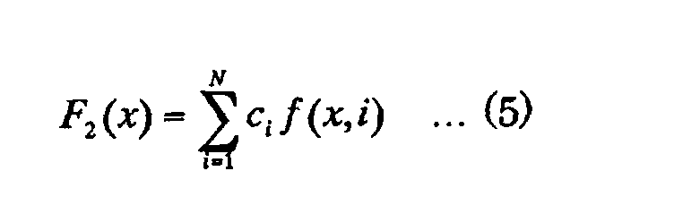
- the desired worked shape can be obtained by performing polishing for the unit time of c i under the i th working condition in each case.
- N is a large value
- the desired worked shape is calculated without performing polishing under these conditions.
- c i is set equal to zero, and the following value is calculated: Then, if the difference between G(x) and F 2 (x) is within permissible limits, this combination of working conditions is employed. Thus, the working conditions can be simplified.
- polishing conditions that constitute elements are determined according to the type of the object of polishing and the type of the final surface shape, after which the combination of polishing conditions that constitute elements is varied according to variations in the shape of the object of polishing prior to polishing. Consequently, the number of polishing conditions constituting elements that are required for each type of object of polishing and each type of final surface shape is not that large; in most cases, several types are sufficient.
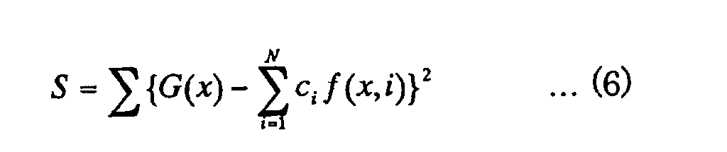
- the combinations of polishing conditions that constitute elements can be determined by utilizing a statistical procedure. For example, it is assumed that x adopts discrete values with ⁇ x as units, and the value of f(x,i) is determined. Then, assuming that c i also adopts discrete values with ⁇ c i as units, the following value corresponding to Equation (3) is determined for all combinations of x , i and c i under these conditions: The range of the initial sigma is the range of x constituting the object of polishing. Furthermore, combinations of c i which are such that S shows a minimum value are determined, and the polishing conditions that constitute elements are then combined on the basis of the processing described above.
- the system may be devised so that the shapes of G(x) and f(x,i) are compared, and the probability of c i being generated as a random number is determined based on the result of this comparison.
- the question in all instances is the time for which the polishing conditions constituting elements should be applied. If the application time is determined, then the question of how this application time is distributed in a time series can be freely determined. For example, in a case where the polishing condition constituting the first element is applied for 3 minutes, and the polishing condition constituting the second element is applied for 2 minutes, the polishing condition constituting the first element may be applied for the first 3 minutes, and the polishing condition constituting the second element may be applied for the next two minutes, or the polishing condition constituting the first element and the polishing condition constituting the second element may be alternately applied for one minute at a time, e.g., in the sequence first ⁇ second ⁇ first ⁇ second ⁇ first.
- both of the polishing conditions constituting elements are applied "as is"; however, polishing may be performed using other polishing conditions in which these polishing conditions constituting elements are combined. An example of this will be described below.
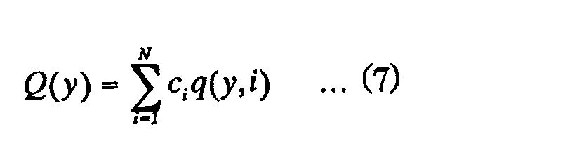
- the method of combining the polishing conditions constituting elements that are to be applied is first determined by the method described above. Since the polishing conditions that constitute the respective elements are determined by the starting position of the swinging of the polishing body on the wafer and the swinging stroke as described above, the time for which the central axis of the polishing body is present in respective positions on the wafer can be calculated from these values. Specifically, in regard to the polishing condition constituting the i th element, the time for which the center position y of the polishing body is present in a given position can be viewed as q(y,i).
- the time Q(y) for which the central axis of the polishing body is present can be expressed as follows using c i determined by the method described above: Accordingly, a polishing method which is such that this Q(y) can be realized may be considered.
- the swinging speed of the polishing body at various positions on the wafer may be varied so that the time for which the central axis of the polishing body is present at y within one swinging time is proportional to Q(y). Specifically, this can be realized by slowing the swinging speed in positions where Q(y) is large, and slowing the swinging speed in positions where Q(y) is small.
- Q(y) can be realized by repeating the swinging a required number of times.
- polishing conditions are determined in this way, the desired worked shape can be obtained by performing polishing in accordance with these conditions.
- the shape input means input the surface shape of the object of polishing prior to polishing, and the target surface shape.
- the target surface shape is supplied by manual input, or is supplied form a higher computer.
- values measured by means of a measuring apparatus are input, or else the surface shape is supplied by manual input or from a higher computer.
- the target surface shape is given for each type of object of polishing.
- the surface shape of the object of polishing prior to polishing is given for each object of polishing or for each lot.
- the shape input means send these input values to the polishing condition determining means.
- polishing condition determining means determine the polishing conditions using the method of the present invention for determining polishing conditions.
- the above-mentioned polishing conditions that constitute elements are given as time series, and the swinging velocity corresponding to the swinging position is determined by converting combinations of the above-mentioned polishing conditions that constitute elements into variations in the swinging velocity of the polishing body (and in this way controlling the time for which the central axis of the polishing body is present).
- the polishing apparatus control means input the polishing conditions determined by the polishing condition determining means, and control the polishing apparatus so that these conditions are realized.
- the polishing condition determination method of the present invention can be realized by means of a computer if the above-mentioned algorithm is used.
- the polishing condition determination method is described as a computer program. If this program is stored on a computer program storage medium, the polishing conditions can be determined using a personal computer, etc. Accordingly, the target polishing can be accomplished by a human being giving commands to the polishing apparatus using these polishing conditions.
- the polishing condition determining means in Figure 1 can be constructed using a computer, and in this case, such a program can be stored on the program storage medium of this computer.
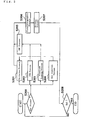
- FIG. 2 is a flow chart which shows the semiconductor device manufacturing process.
- the appropriate treatment process is first selected in step S200 from steps S201 through S204 described below.
- the processing proceeds to one of steps S201 through S204 according to the selection.
- step S201 is an oxidation process in which the surface of the wafer is oxidized.
- Step S202 is a CVD process in which an insulating film is formed on the surface of the wafer by CVD, etc.
- Step S203 is an electrode formation process in which electrodes are formed on the wafer by a process such as evaporation.
- Step S204 is an ion injection process in which ions are injected in the wafer.
- Step S205 is a CMP process.
- the smoothing of an interlayer insulating film, or formation of a damascene by the polishing of the metal film on the surface of a semiconductor device, etc. is performed using the polishing apparatus of the present invention.
- Step S206 is a photolithographic process.
- the coating of the wafer with a resist, the baking of a circuit pattern onto the wafer by exposure using an exposure apparatus, and the development of the exposed wafer are performed.
- the next step S207 is an etching process in which the portions other than the developed resist image are removed by etching, after which the resist is stripped so that the resist that has become unnecessary following the completion of etching is removed.
- step S208 a judgement is made as to whether or not all required processes have been completed, and if these processes have not been completed, the processing returns to step S200, and a circuit pattern is formed on the wafer by repeating the preceding steps. If it is judged in step S208 that all of the processes have been completed, the processing is ended.
- the polishing method according to the present invention is used in the CMP process. Accordingly, wafers having the target surface shape can be manufactured with good yield and in a short period of time. As a result, semiconductor devices can be manufactured at a low cost compared to conventional semiconductor device manufacturing methods.
- the polishing of a wafer with a diameter of 200 mm which had a Cu pattern inside was performed using a polishing apparatus in which the polishing pad was smaller than the wafer.
- This polishing was performed using an annular polishing pad with an external diameter of 150 mm and an internal diameter of 50 mm under the following conditions: head rpm 400 rpm, wafer rpm 200 rpm, polishing time 60 sec, slurry 100 ml (RD98052, FUJIMI Incorporated).
- the wafer had a film thickness of 1.5 ⁇ m, and the initial film thickness was extremely uniform.
- the target amount of polishing was set at 0.44 ⁇ m, and conditions for realizing a flat worked shape were determined by combinations of the above-mentioned six sets of polishing conditions constituting elements.
- the worked shapes obtained when the polishing time was set at three-second increments (5% increments of 60 seconds, which was the polishing time when actual working conditions were obtained), i.e., 3 seconds, 6 seconds, ..., 57 seconds, were first determined for each of the above-mentioned six sets of polishing conditions constituting elements.
- 21 sets of weighted polishing conditions and the worked shapes obtained in the case of these polishing conditions were obtained by adding the initial shape prior to polishing (polishing time of zero seconds) and the worked shape obtained in the case of a polishing time of 60 seconds to the worked shapes corresponding to polishing times of three-second increments obtained by the above-mentioned calculations from a single set of polishing conditions constituting elements.
- polishing times under the respective polishing conditions constituting elements were selected from the above-mentioned 21 sets for each set of polishing conditions constituting elements so that the sum of the polishing times when polishing was performed combining the above-mentioned six sets of polishing conditions constituting elements was 60 seconds, and the worked shapes obtained by all combinations of these polishing elements (e.g., all combinations such as 9 seconds under condition 1, 0 seconds under condition 2, 18 seconds under condition 3, 9 seconds under condition 4, 9 seconds under condition 5, and 15 seconds under condition 6) were determined, thereby discovering a combination of polishing conditions which was such that the sum of the squares of the differences between the determined worked shape and the target worked shape showed a minimum value.
- polishing of 0.44 ⁇ m with a flat worked shape can be obtained if polishing is performed for 12 seconds under condition 1, 12 seconds under condition 3, 6 seconds under condition 4, and 30 seconds under condition 6.
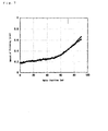
- the polishing profile obtained by these calculated results is shown in Figure 9.
- the horizontal axis indicates the position on the wafer, and the vertical axis indicates the predicted amount of polishing obtained by calculation.
- the target amount of polishing is indicated by a straight line, and the calculated values are indicated by black triangles.
- the number of wafers required in order to determine the polishing conditions was six wafers.
- the time required for the series of operations was 1 hour, including preparation, polishing and measurement.
- FIG. 10 shows the results obtained.
- the horizontal axis indicates the center coordinates of the head (corresponding to the wafer position), and the vertical axis indicates the swinging velocity.
- the triangles indicate the calculated values, and indicate swinging at the corresponding swinging velocity at the specified head center coordinates.
- the pattern shown in Figure 10 indicates swinging at a swinging velocity of 364 mm/min when the head center coordinates are between 23 mm and 38 mm, swinging at a swinging velocity of 1092 mm/min when the head center coordinates are between 38 mm and 53 mm, and swinging at a swinging velocity of 401 mm/min when the head center coordinates are between 53 mm and 68 mm.
- polishing results that were more or less the same as those obtained in Embodiment 1 were obtained in the case of swinging for 7 reciprocating passes.
- the uniformity in this case was 2.5% at 1 ⁇ .
- the polishing of a wafer with a diameter of 200 mm in which a Cu pattern was formed inside was performed using a polishing apparatus in which the polishing pad was smaller than the wafer.
- Cu wafers from a different wafer lot from that used in Embodiment 1 were used in the polishing of this embodiment.
- the wafer of this lot had a protruding shape in which the film thickness of the wafer was 1.6 ⁇ m in the central portion of the wafer, and 1.45 ⁇ m in the edge portions of the wafer.
- the target residual film thickness was set at 0.9 ⁇ m, and conditions for realizing a flat worked shape were determined using combinations of the six sets of polishing conditions constituting elements used in Embodiment 1.
- the simulation method was the same as that used in Embodiment 1. As a result, it was found that polishing for 24 seconds under condition 1, 6 seconds under condition 3 and 30 seconds under condition 4 was favorable. When polishing was performed under these conditions, the residual film thickness was 0.9 ⁇ m, and polishing in which the uniformity of the residual film thickness was extremely high was possible. The uniformity of the residual film was 2.5% at 1 ⁇ .
- the time required for simulation, preparation, polishing and measurement in this series of polishing operations was 20 minutes.
- Embodiment 1 in spite of the fact that polishing was performed with a flat shape as the target shape, the shape that was obtained following actual polishing was as shown in Figure 9. Accordingly, deviations from the target shape in respective wafer positions were calculated, the six sets of polishing condition elements indicated in Embodiment 1 were combined, and a combination was determined which was such that the polished shape obtained as a result of the above-mentioned combinations corresponded to the above-mentioned error components.
- the probability of the presence of the center of the polishing pad was determined as in Embodiment 2 from a new combination of polishing condition elements obtained by adding the above-mentioned combination to the combination obtained in Embodiment 1, and the swinging velocity was determined from this probability of the presence of the center of the polishing pad.
- the six polishing condition elements used in Embodiment 1 were respectively subjected to a Fourier transform; furthermore, the amounts of polishing in respective portions of the wafer in a case where the residual film thickness was set at 0.9 ⁇ m were determined, and these polishing amounts were also subjected to a Fourier transform. Then, weighting was determined by the method of least squares so that the conditions obtained by adding this weighting to the six polishing condition elements that had been subjected to a Fourier transform most closely approached the values obtained by subjecting the polishing amounts to a Fourier transform.
- the polishing of a wafer with a diameter of 200 mm in which a Cu pattern was formed inside was performed using a polishing apparatus in which the polishing pad was smaller than the wafer.
- This polishing was performed using an annular polishing pad with an external diameter of 150 mm and an internal diameter of 50 mm under the following conditions: head rpm 400 rpm, wafer rpm 200 rpm, polishing time 60 sec, slurry 100 ml (RD98052, FUJIMI Incorporated). These are the same conditions as in Embodiment 1.
- the initial film thickness of the wafer showed an extremely high uniformity.
- the polishing conditions for realizing polishing that would produce a flat worked shape in one step using this wafer were determined by trial and error. 20 wafers were required in order to determine these conditions. The time required in order to determine the conditions was 4 hours.
- the polishing of a wafer with a diameter of 200 mm in which a Cu pattern was formed inside was performed using a polishing apparatus characterized by the fact that the polishing pad was smaller than the wafer.
- This polishing was performed using an annular polishing pad with an external diameter of 150 mm and an internal diameter of 50 mm under the following conditions: head rpm 400 rpm, wafer rpm 200 rpm, polishing time 60 sec, slurry 100 ml (RD98052, FUJIMI Incorporated). These are the same conditions as in Embodiment 1.
- the initial film thickness of the wafer used in this case had a protruding shape in which the film thickness of the center shape was large.
- the polishing conditions for realizing a uniform residual film thickness using this wafer were determined by trial and error. 20 wafers were required in order to determine these conditions. The time required in order to determine the conditions was 6 hours.
- the actual polishing conditions can be determined in most instances by using polishing conditions constituting elements prepared initially as basic conditions in common, and determining combinations of these conditions by simulation even if the shape that is to be worked varies. Accordingly, even in cases where a new worked shape is required, there is no need to determine the polishing conditions by trial and error each time.
- the present invention can be used to predict the worked shape, determine the working conditions and perform actual working in cases where mechanical working such as polishing or grinding is performed.
Landscapes
- Engineering & Computer Science (AREA)
- Mechanical Engineering (AREA)
- Mechanical Treatment Of Semiconductor (AREA)
- Finish Polishing, Edge Sharpening, And Grinding By Specific Grinding Devices (AREA)
- Grinding And Polishing Of Tertiary Curved Surfaces And Surfaces With Complex Shapes (AREA)
- Constituent Portions Of Griding Lathes, Driving, Sensing And Control (AREA)
Abstract
Description


Claims (16)
- A method for predicting the worked shape that is obtained in cases where an object of working is worked by causing relative motion to take place between a tool and the above-mentioned object of working in a sate in which abrasive grains are interposed between the above-mentioned tool and object of working, this worked shape prediction method being characterized by the fact that the relationship between working conditions that constitute elements and the elements of the worked shape that is obtained when working is performed under these working conditions is determined in advance, and when specified working conditions are given, these working conditions are broken down into combinations of working conditions constituting the above-mentioned elements, and the sum of the worked shape elements that are obtained by means of the above-mentioned combinations are taken as the predicted worked shape that will be obtained when working is performed under the above-mentioned specified working conditions.
- The worked shape prediction method according to Claim 1, which is characterized by the fact that the above-mentioned worked shape elements are subjected to a Fourier transform, the sum of the worked shape elements determined using the above-mentioned combinations are determined as the sum of the Fourier-transformed functions for these combinations, and the predicted worked shape is obtained by subjecting the results to an inverse Fourier transform.
- The worked shape prediction method according to Claim 1 or Claim 2, which is characterized by the fact that the above-mentioned object of working is larger than the above-mentioned tool.
- A method for determining the working conditions that will work the object of working into a specified shape in a working apparatus in which such an object of working is worked by causing relative motion to take place between a tool and the above-mentioned object of working in a state in which abrasive grains are interposed between this tool and object of working, this method for determining working conditions being characterized by the fact that the relationship between working conditions constituting elements and the elements of the worked shape that is obtained when working is performed under these working conditions is determined beforehand, combinations of the above-mentioned working conditions constituting elements are determined which are such that the combinations of these worked shape elements approach the above-mentioned specified shape, and these combinations are taken as the working conditions.
- The working condition determination method according to Claim 4, which is characterized by the fact that the above-mentioned worked shape elements are subjected to a Fourier transform, the above-mentioned specified shape is subjected to a Fourier transform, combinations of the above-mentioned working conditions constituting elements are determined which are such that the combinations of the Fourier-transformed values of the worked shape elements approach the Fourier-transformed value of the above-mentioned specified shape, and these combinations are taken as the working conditions.
- The working condition determination method according to Claim 4 or Claim 5, which is characterized by the fact that the above-mentioned combinations of working conditions that constitute elements are combinations in which the respective working conditions constituting elements are combined in a time series.
- The working condition determination method according to Claim 4 or Claim 5, which is characterized by the fact that the working conditions obtained by means of combinations of the above-mentioned working conditions constituting elements are working conditions obtained by weighting and combining the respective working conditions constituting elements.
- The working condition determination method according to Claim 7, which is characterized by the fact that the working conditions obtained by means of combinations of the above-mentioned working conditions that constitute elements are taken as functions of the swinging position of the above-mentioned tool or the above-mentioned object of working.
- The working condition determination method according to Claim 4 or Claim 5, which is characterized by the fact that the above-mentioned combinations of the working conditions that constitute elements consist of combinations obtained by combining respective working conditions that constitute elements in time series, and combinations obtained by applying weighting and combining respective working conditions that constitute elements.
- The working condition determination method according to any one of Claims 4 through 9, which is characterized by the fact that combinations of the above-mentioned working conditions that constitute elements are determined so that the combination of the above-mentioned worked shape elements approach the above-mentioned specified shape, working is performed using these combinations as the working conditions, the error between the actual worked shape and the above-mentioned specified shape is determined, and working conditions obtained by adding combinations of worked shape elements that compensate for this error to the above-mentioned combinations of worked shape elements are taken as the new working conditions.
- The working condition determination method according to any one of Claims 4 through 10, which is characterized by the fact that above-mentioned object of working is larger than the above-mentioned tool.
- A working method in which an object of working is worked by causing relative motion to take place between a tool and this object of working in a state in which abrasive grains are interposed between this tool and object of working, this working method being characterized by the fact that the working conditions are determined by the working condition determination method according to any one of Claims 4 through 11.
- A working system using a working apparatus in which an object of working is worked by causing relative motion to take place between a tool and this object of working in a state in which abrasive grains are interposed between this tool and object of working, this working system being characterized by the fact that the system has means for inputting the surface shape of the above-mentioned object of working prior to working, and the target surface shape of the above-mentioned object of working following working, means for determining the working conditions by the working condition determination method according to any one of Claims 4 through 11, and means for controlling the above-mentioned working apparatus in accordance with the determined working conditions.
- A semiconductor device manufacturing method which is characterized by the fact that this method has a process in which wafers are worked using the working method according to Claim 12 or the working system according to Claim 13.
- A computer program which describes the working condition determination method according to any one of Claims 4 through 11.
- A computer program storage medium which stores the computer program according to Claim 15.
Applications Claiming Priority (5)
| Application Number | Priority Date | Filing Date | Title |
|---|---|---|---|
| JP2001024882 | 2001-01-31 | ||
| JP2001024882 | 2001-01-31 | ||
| JP2001268410 | 2001-09-05 | ||
| JP2001268610A JP5002875B2 (en) | 2001-01-31 | 2001-09-05 | Processing shape prediction method, processing condition determination method, processing method, processing system, semiconductor device manufacturing method, computer program, and computer program storage medium |
| PCT/JP2002/000182 WO2002061817A1 (en) | 2001-01-31 | 2002-01-15 | Working shape prediction method, working requirement determination method, working method, working system, method of manufacturing semiconductor device, computer program, and computer program storage medium |
Publications (3)
| Publication Number | Publication Date |
|---|---|
| EP1365445A1 true EP1365445A1 (en) | 2003-11-26 |
| EP1365445A4 EP1365445A4 (en) | 2006-11-22 |
| EP1365445B1 EP1365445B1 (en) | 2007-12-05 |
Family
ID=26608725
Family Applications (1)
| Application Number | Title | Priority Date | Filing Date |
|---|---|---|---|
| EP02737613A Expired - Lifetime EP1365445B1 (en) | 2001-01-31 | 2002-01-15 | Working shape prediction method, working requirement determination method, working method, working system, method of manufacturing semiconductor device, computer program, and computer program storage medium |
Country Status (8)
| Country | Link |
|---|---|
| US (2) | US7686673B2 (en) |
| EP (1) | EP1365445B1 (en) |
| JP (1) | JP5002875B2 (en) |
| KR (1) | KR100846685B1 (en) |
| CN (1) | CN1225010C (en) |
| DE (1) | DE60223905T2 (en) |
| TW (1) | TW521341B (en) |
| WO (1) | WO2002061817A1 (en) |
Families Citing this family (12)
| Publication number | Priority date | Publication date | Assignee | Title |
|---|---|---|---|---|
| JP5002875B2 (en) * | 2001-01-31 | 2012-08-15 | 株式会社ニコン | Processing shape prediction method, processing condition determination method, processing method, processing system, semiconductor device manufacturing method, computer program, and computer program storage medium |
| AU2003221430A1 (en) * | 2002-03-20 | 2003-09-29 | Nikon Corporation | Treatment condition decision method, treatment condition decision system, treatment system, treatment condition decision calculator program, program recording medium, and semiconductor device manufacturing method |
| WO2006106790A1 (en) * | 2005-04-01 | 2006-10-12 | Nikon Corporation | Polishing apparatus, semiconductor device manufacturing method using such polishing apparatus and semiconductor device manufactured by such semiconductor device manufacturing method |
| JP2009140956A (en) * | 2007-12-03 | 2009-06-25 | Elpida Memory Inc | Shape prediction simulator, method and program |
| CN102380816A (en) * | 2010-08-30 | 2012-03-21 | 旺宏电子股份有限公司 | Chemical mechanical polishing method and system |
| CN102975110A (en) * | 2012-12-26 | 2013-03-20 | 上海宏力半导体制造有限公司 | Chemical and mechanical grinding rate control method |
| JP2016058724A (en) * | 2014-09-11 | 2016-04-21 | 株式会社荏原製作所 | Processing module, processing apparatus, and processing method |
| KR102218204B1 (en) | 2015-01-19 | 2021-02-23 | 가부시키가이샤 에바라 세이사꾸쇼 | Polishing-amount simulation method for buffing process, and buffing device |
| CN107887265A (en) * | 2016-09-23 | 2018-04-06 | 清华大学 | The polishing method of polissoir |
| CN111421462B (en) * | 2019-01-08 | 2022-03-22 | 中芯国际集成电路制造(上海)有限公司 | chemical mechanical polishing method |
| JP7427333B2 (en) * | 2020-03-18 | 2024-02-05 | 株式会社ディスコ | Edge alignment method |
| CN115771102B (en) * | 2022-11-30 | 2024-02-27 | 大连理工大学 | A digital twin system applied to double-sided grinding process |
Family Cites Families (21)
| Publication number | Priority date | Publication date | Assignee | Title |
|---|---|---|---|---|
| US5460034A (en) * | 1992-07-21 | 1995-10-24 | The United States Of America As Represented By The Secretary Of The Air Force | Method for measuring and analyzing surface roughness on semiconductor laser etched facets |
| US5599423A (en) * | 1995-06-30 | 1997-02-04 | Applied Materials, Inc. | Apparatus and method for simulating and optimizing a chemical mechanical polishing system |
| JP3580036B2 (en) | 1996-08-06 | 2004-10-20 | ソニー株式会社 | Polishing simulation method |
| JP2001501545A (en) * | 1996-10-04 | 2001-02-06 | オブシディアン,インコーポレイテッド | Method and system for controlling chemical mechanical polishing thickness removal |
| JPH1174235A (en) * | 1997-08-29 | 1999-03-16 | Sony Corp | Polishing simulation |
| JPH11126765A (en) | 1997-10-22 | 1999-05-11 | Toshiba Corp | Polishing simulation method, recording medium recording polishing simulation method, and polishing method |
| JPH11207607A (en) * | 1998-01-22 | 1999-08-03 | Japan Energy Corp | Polishing method and InP substrate |
| JP2000005988A (en) * | 1998-04-24 | 2000-01-11 | Ebara Corp | Polishing equipment |
| US6271047B1 (en) * | 1998-05-21 | 2001-08-07 | Nikon Corporation | Layer-thickness detection methods and apparatus for wafers and the like, and polishing apparatus comprising same |
| US6241847B1 (en) * | 1998-06-30 | 2001-06-05 | Lsi Logic Corporation | Method and apparatus for detecting a polishing endpoint based upon infrared signals |
| JP2000024914A (en) * | 1998-07-03 | 2000-01-25 | Hitachi Ltd | Polishing device for semiconductor wafer |
| US6169931B1 (en) * | 1998-07-29 | 2001-01-02 | Southwest Research Institute | Method and system for modeling, predicting and optimizing chemical mechanical polishing pad wear and extending pad life |
| JP2000254860A (en) * | 1999-03-08 | 2000-09-19 | Nikon Corp | Polishing equipment |
| JP2001237206A (en) * | 1999-12-15 | 2001-08-31 | Matsushita Electric Ind Co Ltd | Flattening method |
| US20020013122A1 (en) * | 1999-12-22 | 2002-01-31 | Nikon Corporation | Process and apparatus for chemimechanically polishing a substrate |
| US6449524B1 (en) * | 2000-01-04 | 2002-09-10 | Advanced Micro Devices, Inc. | Method and apparatus for using equipment state data for run-to-run control of manufacturing tools |
| JP2001219369A (en) * | 2000-02-08 | 2001-08-14 | Sumitomo Metal Ind Ltd | Polishing shape prediction method, polishing method and polishing apparatus |
| US6290572B1 (en) * | 2000-03-23 | 2001-09-18 | Micron Technology, Inc. | Devices and methods for in-situ control of mechanical or chemical-mechanical planarization of microelectronic-device substrate assemblies |
| JP5002875B2 (en) * | 2001-01-31 | 2012-08-15 | 株式会社ニコン | Processing shape prediction method, processing condition determination method, processing method, processing system, semiconductor device manufacturing method, computer program, and computer program storage medium |
| US6821794B2 (en) * | 2001-10-04 | 2004-11-23 | Novellus Systems, Inc. | Flexible snapshot in endpoint detection |
| JP3784330B2 (en) * | 2002-01-30 | 2006-06-07 | 株式会社ジェイテクト | NC data correction method for generating grinding for controlling numerically controlled grinding machine and numerically controlled grinding machine for implementing the method |
-
2001
- 2001-09-05 JP JP2001268610A patent/JP5002875B2/en not_active Expired - Lifetime
- 2001-12-28 TW TW90132696A patent/TW521341B/en not_active IP Right Cessation
-
2002
- 2002-01-15 WO PCT/JP2002/000182 patent/WO2002061817A1/en not_active Ceased
- 2002-01-15 KR KR20037007829A patent/KR100846685B1/en not_active Expired - Lifetime
- 2002-01-15 US US10/470,537 patent/US7686673B2/en not_active Expired - Lifetime
- 2002-01-15 DE DE2002623905 patent/DE60223905T2/en not_active Expired - Lifetime
- 2002-01-15 CN CNB028034392A patent/CN1225010C/en not_active Expired - Lifetime
- 2002-01-15 EP EP02737613A patent/EP1365445B1/en not_active Expired - Lifetime
-
2010
- 2010-03-29 US US12/749,306 patent/US9031687B2/en not_active Expired - Fee Related
Also Published As
| Publication number | Publication date |
|---|---|
| JP2002305165A (en) | 2002-10-18 |
| DE60223905T2 (en) | 2008-11-13 |
| EP1365445B1 (en) | 2007-12-05 |
| TW521341B (en) | 2003-02-21 |
| KR20030074653A (en) | 2003-09-19 |
| US20100233937A1 (en) | 2010-09-16 |
| WO2002061817A1 (en) | 2002-08-08 |
| CN1225010C (en) | 2005-10-26 |
| KR100846685B1 (en) | 2008-07-16 |
| US20040053558A1 (en) | 2004-03-18 |
| JP5002875B2 (en) | 2012-08-15 |
| CN1484851A (en) | 2004-03-24 |
| DE60223905D1 (en) | 2008-01-17 |
| US9031687B2 (en) | 2015-05-12 |
| US7686673B2 (en) | 2010-03-30 |
| EP1365445A4 (en) | 2006-11-22 |
Similar Documents
| Publication | Publication Date | Title |
|---|---|---|
| US9031687B2 (en) | Method for predicting worked shape, method for determining working conditions, working method, working system, semiconductor device manufacturing method, computer program and computer program storage medium | |
| KR100572039B1 (en) | Systems and methods for controlling the manufacture of individual components in semiconductor manufacturing using model predictive control | |
| US7878882B2 (en) | Advanced workpiece finishing | |
| US7037172B1 (en) | Advanced wafer planarizing | |
| Hu et al. | Application of run by run controller to the chemical-mechanical planarization process. II | |
| US7086927B2 (en) | Methods and systems for planarizing workpieces, e.g., microelectronic workpieces | |
| KR100471184B1 (en) | System and method for controlling polishing time of multi-layer in chemical mechanical polishing process | |
| US6884147B2 (en) | Method for chemical-mechanical polish control in semiconductor manufacturing | |
| JP5686148B2 (en) | Processing condition determination method and semiconductor device manufacturing method | |
| Boning et al. | Pattern dependent modeling for CMP optimization and control | |
| US6530822B1 (en) | Method for controlling polishing time in chemical-mechanical polishing process | |
| US6534328B1 (en) | Method of modeling and controlling the endpoint of chemical mechanical polishing operations performed on a process layer, and system for accomplishing same | |
| CN100366386C (en) | Method and apparatus for controlling chemical mechanical polishing of a substrate | |
| JP2004532510A (en) | Chemical mechanical polishing method for copper-oxide damascene structure | |
| JP4333166B2 (en) | Processing shape prediction method, processing condition determination method, processing amount prediction method, processing shape prediction system, processing condition determination system, processing system, processing shape prediction computer program, processing condition determination computer program, program recording medium, and semiconductor device Production method | |
| US7575501B1 (en) | Advanced workpiece finishing | |
| JP3745951B2 (en) | Chemical mechanical polishing method and chemical mechanical polishing apparatus | |
| US20070082490A1 (en) | Apparatus of chemical mechanical polishing and chemical mechanical polishing process | |
| Lin et al. | Chemical mechanical planarization operation via dynamic programming | |
| TWI286961B (en) | Methods of predicting CMP removal rate and transferring CMP processes | |
| JPWO2003078104A1 (en) | Processing condition determination method, processing condition determination system, processing system, processing condition determination computer program, program recording medium, and semiconductor device manufacturing method | |
| Kumar | Agent based diagnostic system for the defect analysis during chemical mechanical polishing (CMP) | |
| Oji | Characterization and modeling of uniformity in chemical mechanical polishing |
Legal Events
| Date | Code | Title | Description |
|---|---|---|---|
| PUAI | Public reference made under article 153(3) epc to a published international application that has entered the european phase |
Free format text: ORIGINAL CODE: 0009012 |
|
| 17P | Request for examination filed |
Effective date: 20030731 |
|
| AK | Designated contracting states |
Kind code of ref document: A1 Designated state(s): AT BE CH CY DE DK ES FI FR GB GR IE IT LI LU MC NL PT SE TR |
|
| A4 | Supplementary search report drawn up and despatched |
Effective date: 20061019 |
|
| RIC1 | Information provided on ipc code assigned before grant |
Ipc: B24B 37/04 20060101AFI20061013BHEP Ipc: B24B 49/00 20060101ALI20061013BHEP |
|
| GRAJ | Information related to disapproval of communication of intention to grant by the applicant or resumption of examination proceedings by the epo deleted |
Free format text: ORIGINAL CODE: EPIDOSDIGR1 |
|
| GRAP | Despatch of communication of intention to grant a patent |
Free format text: ORIGINAL CODE: EPIDOSNIGR1 |
|
| RBV | Designated contracting states (corrected) |
Designated state(s): DE FR GB NL |
|
| GRAS | Grant fee paid |
Free format text: ORIGINAL CODE: EPIDOSNIGR3 |
|
| GRAA | (expected) grant |
Free format text: ORIGINAL CODE: 0009210 |
|
| AK | Designated contracting states |
Kind code of ref document: B1 Designated state(s): DE FR GB NL |
|
| REG | Reference to a national code |
Ref country code: GB Ref legal event code: FG4D |
|
| REF | Corresponds to: |
Ref document number: 60223905 Country of ref document: DE Date of ref document: 20080117 Kind code of ref document: P |
|
| ET | Fr: translation filed | ||
| PLBE | No opposition filed within time limit |
Free format text: ORIGINAL CODE: 0009261 |
|
| STAA | Information on the status of an ep patent application or granted ep patent |
Free format text: STATUS: NO OPPOSITION FILED WITHIN TIME LIMIT |
|
| 26N | No opposition filed |
Effective date: 20080908 |
|
| PGFP | Annual fee paid to national office [announced via postgrant information from national office to epo] |
Ref country code: GB Payment date: 20100113 Year of fee payment: 9 |
|
| REG | Reference to a national code |
Ref country code: NL Ref legal event code: V1 Effective date: 20110801 |
|
| GBPC | Gb: european patent ceased through non-payment of renewal fee |
Effective date: 20110115 |
|
| PG25 | Lapsed in a contracting state [announced via postgrant information from national office to epo] |
Ref country code: GB Free format text: LAPSE BECAUSE OF NON-PAYMENT OF DUE FEES Effective date: 20110115 |
|
| PG25 | Lapsed in a contracting state [announced via postgrant information from national office to epo] |
Ref country code: NL Free format text: LAPSE BECAUSE OF NON-PAYMENT OF DUE FEES Effective date: 20110801 |
|
| PGFP | Annual fee paid to national office [announced via postgrant information from national office to epo] |
Ref country code: NL Payment date: 20100131 Year of fee payment: 9 |
|
| REG | Reference to a national code |
Ref country code: FR Ref legal event code: PLFP Year of fee payment: 15 |
|
| REG | Reference to a national code |
Ref country code: FR Ref legal event code: PLFP Year of fee payment: 16 |
|
| REG | Reference to a national code |
Ref country code: FR Ref legal event code: PLFP Year of fee payment: 17 |
|
| PGFP | Annual fee paid to national office [announced via postgrant information from national office to epo] |
Ref country code: FR Payment date: 20201210 Year of fee payment: 20 |
|
| PGFP | Annual fee paid to national office [announced via postgrant information from national office to epo] |
Ref country code: DE Payment date: 20210105 Year of fee payment: 20 |
|
| REG | Reference to a national code |
Ref country code: DE Ref legal event code: R071 Ref document number: 60223905 Country of ref document: DE |