EP1363423A2 - Data signal quality evaluation method and apparatus using high speed sampling - Google Patents
Data signal quality evaluation method and apparatus using high speed sampling Download PDFInfo
- Publication number
- EP1363423A2 EP1363423A2 EP03101315A EP03101315A EP1363423A2 EP 1363423 A2 EP1363423 A2 EP 1363423A2 EP 03101315 A EP03101315 A EP 03101315A EP 03101315 A EP03101315 A EP 03101315A EP 1363423 A2 EP1363423 A2 EP 1363423A2
- Authority
- EP
- European Patent Office
- Prior art keywords
- data
- signal
- data signal
- electrical
- quality evaluation
- Prior art date
- Legal status (The legal status is an assumption and is not a legal conclusion. Google has not performed a legal analysis and makes no representation as to the accuracy of the status listed.)
- Granted
Links
Images


Classifications
-
- H—ELECTRICITY
- H04—ELECTRIC COMMUNICATION TECHNIQUE
- H04L—TRANSMISSION OF DIGITAL INFORMATION, e.g. TELEGRAPHIC COMMUNICATION
- H04L1/00—Arrangements for detecting or preventing errors in the information received
- H04L1/24—Testing correct operation
-
- H—ELECTRICITY
- H04—ELECTRIC COMMUNICATION TECHNIQUE
- H04B—TRANSMISSION
- H04B10/00—Transmission systems employing electromagnetic waves other than radio-waves, e.g. infrared, visible or ultraviolet light, or employing corpuscular radiation, e.g. quantum communication
- H04B10/07—Arrangements for monitoring or testing transmission systems; Arrangements for fault measurement of transmission systems
- H04B10/075—Arrangements for monitoring or testing transmission systems; Arrangements for fault measurement of transmission systems using an in-service signal
- H04B10/079—Arrangements for monitoring or testing transmission systems; Arrangements for fault measurement of transmission systems using an in-service signal using measurements of the data signal
- H04B10/0795—Performance monitoring; Measurement of transmission parameters
- H04B10/07953—Monitoring or measuring OSNR, BER or Q
Definitions
- the present invention relates to a data signal quality evaluation method using high speed sampling, suitable for use when sampling an optical or electrical data signal with a predetermined bit rate and displaying an eye-diagram and measuring signal quality.
- FIG. 10 A first example of a conventional optical signal quality evaluation apparatus is shown in FIG. 10 (see reference document "Handbook of ELECTRONIC TEST EQUIPMENT (Section 5-8. SAMPLING OSCILLOSCOPE), pp. 184-189, JOHN D. LENK, Prentice-Hall, Inc., Englewood Cliffs, N. J., 1971", reference document “Modeling of the HP-1430A Feedthrough Wide-Band (28-ps) Sampling Head, SEDKI M. RIAD, IEEE Transactions on Instrumentation and Measurement, Vol. IM-31, No. 2, June 1982, pp. 110-115", for example).
- the electrical signal processing device 104 samples the electric intensity modulated signal input via the clock extraction device 102 in accordance with the sampling clock, and displays a sampled data distribution sequentially based on the obtained sampled electrical signal, thereby obtaining a signal eye-diagram, and evaluates the optical signal quality parameters.
- optical sampling devices are provided before the opto-electric conversion device.
- an optical splitter splits the optical signal, and optical sampling is performed using a sampling clock or a sampling optical pulse train synchronized with the clock obtained by performing clock extraction from one of the split optical signals.
- the sampled optical signal is then converted into a sampled electrical signal by the opto-electric conversion device.
- the electrical signal processing device displays sequentially a sampled data distribution based on the obtained sampled electrical signal, thereby obtaining a signal eye-diagram, and evaluates the optical signal quality parameters.
- the repetition frequency of the sampling clock in the first conventional example is normally within the range of several dozen to several hundred kHz , and it takes time to obtain a signal eye-diagram which is necessary and sufficient for evaluation, and therefore wander of the optical signal becomes an issue. Consequently, clock extraction was essential.
- the repetition frequency of the sampling clock or the sampling optical pulse train is approximately 10 MHz, but because it is necessary to perform the electrical signal processing to determine the sampled data distribution sequentially, the effective sampling rate decreases, and it takes time to obtain a necessary and sufficient signal eye-diagram for evaluation, and therefore wander of the optical signal becomes an issue. Consequently, clock extraction was essential.
- An optical signal monitoring apparatus using asynchronous sampling (see European Patent Application Publication No. EP 0920150 A2, reference document "Optical signal quality monitoring method based on optical sampling, I. Shake, H. Takara, S. Kawanishi and Y. Yamabayashi, Electronics Letters, Vol. 34, No. 22, 29th October 1998, pp. 2152-2154", for example), is proposed as a third conventional example, as an optical signal monitoring apparatus which does not require clock extraction.
- this method evaluates an optical signal intensity distribution based on an asynchronous eye-diagram, it still cannot be applied to degradation in the time domain (such as jitter and polarization dispersion).
- an object of the present invention is to provide a data signal quality evaluation method and apparatus which by omitting a clock extraction section, enables the scale of the apparatus to be reduced, which allows the method or the apparatus to be simplified, and which allows the cost of the apparatus to be reduced, and which is capable of monitoring not only signal-to-noise ratio ( SNR ) degradation and wavelength dispersion degradation, but also signal quality degradation in the time domain, such as jitter and polarization dispersion degradation.
- SNR signal-to-noise ratio
- the data signal quality evaluation method of the present invention comprises the steps of: after repeating N times (where N is a natural number) a process in which an input optical or electrical data signal with a bit rate of f 0 ( bit / s ) is sampled using an optical or electrical sampling pulse train, which is generated independently of the data signal, and which has a repetition frequency f 1 (Hz) which differs from the bit rate f 0 ( bit / s ), a thus obtained optical or electrical sampled signal is converted into a piece of electrical digital data, and the piece of the electrical digital data is stored in a buffer, reading N pieces of the electrical digital data stored in the buffer at once or sequentially and performing electrical signal processing of the N pieces of the electrical digital data, to obtain a signal eye-diagram and to perform data signal waveform measurement and quality evaluation.
- N is a natural number
- the data signal quality evaluation apparatus of the present invention comprises a sampling pulse train generation device which generates an optical or electrical sampling pulse train, independently of an input optical or electrical data signal with a bit rate of f 0 ( bit / s ), and which has a repetition frequency f 1 (Hz) which differs from the bit rate f 0 ( bit / s ); a data signal sampling device which samples the data signal with the bit rate f 0 ( bit / s ) in accordance with the sampling pulse train to obtain a sampled signal; a voltage retaining device which converts the sampled signal which is an optical or electrical sampled signal obtained by means of the data signal sampling device into a piece of electrical digital data, and stores a plurality of pieces of the electrical digital data; an electrical signal processing device which reads the plurality of pieces of the electrical digital data stored in the voltage retaining device at once or sequentially to obtain a signal eye-diagram and to evaluate optical data signal quality parameters; and a trigger signal generation device which applies triggers indicating the start/finish of data acquisition
- the present invention can provide a data signal quality evaluation method and apparatus, in which a reduction in the scale of the apparatus, simplification of the method and the apparatus, and a reduction in the cost of the apparatus can be achieved due to the fact that a clock extraction section is omitted, and in which by acquiring data using high speed sampling and a buffer, a pseudo-synchronized optical signal eye-diagram unaffected by wander can be obtained despite the lack of a synchronizing device, and which can monitor not only signal-to-noise ratio ( SNR ) degradation and wavelength dispersion degradation, but also signal quality degradation in the time domain, such as jitter and polarization dispersion degradation.
- SNR signal-to-noise ratio
- the present invention can be applied to a wider range of optical signal bit rates than methods in which electrical sampling methods are used.
- FIG. 1 A first embodiment of a data signal quality evaluation apparatus according to the present invention is shown in FIG. 1. This embodiment is in accordance with the invention as disclosed in claim 10.
- an electrical signal electrical sampling device 12 is used as the data signal sampling device.
- the input data signal is an electrical data signal
- a sampling clock generation device 13 is used as the sampling pulse train generation device.
- FIG. 1 shows a specific case in which an optical signal with a bit rate f 0 ( bit / s ) is converted into an electric intensity modulated signal via an opto-electric conversion device 11 and then input into the electrical signal electrical sampling device 12.
- the opto-electric conversion device 11 is unnecessary, and such an embodiment is also included in the present embodiment. The operation of the present embodiment is described below.
- the optical signal with a bit rate f 0 ( bit / s ) arrives at the electrical signal electrical sampling device 12 via the opto-electric conversion device 11 as an electric intensity modulated signal.
- the electrical signal electrical sampling device 12 samples the electric intensity modulated signal in accordance with this sampling clock to obtain a sampled electrical signal.
- a voltage retaining device 14 performs analog/digital conversion (A/D conversion) of the sampled electrical signal according to trigger signals from a trigger signal generation device 15 indicating the start of data acquisition, and a temporary memory storage operation is performed.
- the voltage retaining device 14 stores a plurality of pieces of sampled data for the time until a trigger signal indicating the finish of data acquisition is sent from the trigger signal generation device 15.
- the plurality of pieces of the sampled data are then output according to a trigger signal from an external source.
- a high-speed A/D conversion circuit which comprises an electrical buffer memory with a capacity equal to or greater than a kilobyte and which has the function of MHz to GHz sampling could be used.
- the sampling gate width of the sampling clock is preferably less than 1/4 or thereabouts of the time determined by the reciprocal of the bit rate f 0 of the optical signal.
- the trigger signal generation device 15 sends a trigger signal indicating the start of data read to an electrical signal processing device 16.
- the electrical signal processing device 16 reads the plurality of pieces of the sampled data from the voltage retaining device 14 according to the trigger signal indicating the start of data read, obtains a signal eye-diagram from the plurality of pieces of the sampled data, and performs such functions as displaying the signal eye-diagram and performing predetermined arithmetic processing relating to signal-to-noise ratio ( SNR ) degradation, wavelength dispersion degradation, and signal quality degradation in the time domain such as jitter and polarization dispersion degradation and displaying the results of the predetermined arithmetic processing so that the optical signal quality parameters can be evaluated, or outputting the results to a predetermined external device.
- SNR signal-to-noise ratio
- the repetition frequency f 1 of the sampling clock is determined based only on the number ( n / m ) f 1 which is related to the optical signal bit rate f 0 , and is not made to follow the bit phase of the optical signal using clock extraction or the like.
- the optical signal bit rate is one of either 2.5 Gbit / s , 10 Gbit / s or 40 Gbit / s is considered.
- f 1 can be determined based on this figure.
- the repetition frequency of the sampling clock is set to (100 MHz + a Hz) , and it is assumed that 15000 pieces of sampled data are required, then a data acquisition time of approximately 150 ⁇ s is required.
- the only bit phase shift caused by wander which affects the eye-diagram used in the evaluation is the variation within approximately 150 ⁇ s . If the temperature difference within one day is 60 °C (over 12 hours), then the temperature variation within 150 ⁇ s is approximately 2.1 ⁇ 10 - 7 °C .
- the maximum amount of pulse delay in a nylon coated quartz fiber which forms the transmission line of the optical signal is approximately 0.2 ps / m / °C (actual measured value)
- the amount of pulse delay caused by variation in the temperature of the whole transmission line of 100 km according to air temperature variation is 4.2 ⁇ 10 -3 ps within 150 ⁇ s . Because this value is small enough to be ignored not only in electrical sampling at a resolution of approximately 20 ps but even in optical signal optical sampling at a resolution of approximately 1 ps , the eye-diagram according to the present method can be evaluated as if it is a synchronous eye-diagram.
- An example of a suitable range for setting the offset frequency a is (where k and q are natural numbers) for example.
- the input signal (data signal) in the data signal quality evaluation apparatus of the present invention is not limited to an optical signal with a bit rate f 0 ( bit / s ) as described above, and may be an electrical signal with a bit rate f 0 ( bit / s ).
- the opto-electric conversion device 11 may be omitted, and the input electrical signal with a bit rate f 0 input directly into the electrical signal electrical sampling device 12, for example.
- the plurality of pieces of the sampled data may be read at once, or sequentially.
- FIG. 2 A second embodiment of a data signal quality evaluation apparatus of the present invention is shown in FIG. 2. This embodiment is in accordance with the invention as disclosed in claim 10.
- an optical signal electrical sampling device 22 is used as the data signal sampling device.
- the input data signal is an optical data signal
- a sampling clock generation device 23 is used as the sampling pulse train generation device.
- a sampled optical signal is obtained by the optical signal electrical sampling device 22, then in order to convert the sampled signal into a piece of electrical digital data and store the piece of the electrical digital data, it is necessary to perform analog/digital conversion after performing opto-electric conversion. Consequently, the construction shown in FIG.
- FIG. 2 is such that a voltage retaining device 14 having an analog/digital conversion function is provided after the opto-electric conversion device 21.
- FIG. 2 those structural elements which are the same as in FIG. 1 are given the same reference numerals. The operation of the present embodiment is described below.
- An optical signal with a bit rate of f 0 ( bit / s ) arrives at the optical signal electrical sampling device 22.
- devices such as electrical short pulse generation by means of a combination of a synthesized signal generator and a comb generator can be used as the sampling clock generation device 23.
- the repetition frequency f 1 of the sampling clock is high-speed, in the MHz to GHz region.
- the frequency band of the comb generator is extended to approximately four times the bit rate f 0 of the optical signal, and that the pulse width of the electrical short pulse is set to approximately the time width as determined by the Fourier transform of the frequency band of the comb generator.
- an electric amplifier could be used before or after the comb generator as needed.
- a baseband clipper could be used after the comb generator as needed.
- the optical signal is sampled in accordance with the sampling clock to obtain a sampled optical signal with a bit rate f 1 .
- a gate operation performed by an electro-absorption optical modulator, or the like may be used.
- the transmission band of the optical signal of the optical signal electrical sampling device 22 is preferably close to the optical signal bit rate f 0 .
- the sampling gate width of the optical signal electrical sampling device 22 is preferably equal to or less than 1/4 or thereabouts of the time determined by the reciprocal of the bit rate f 0 of the optical signal.
- the sampled optical signal is then converted into a sampled electrical signal by the opto-electric conversion device 21.
- the voltage retaining device 14 performs analog/digital conversion (AID conversion) of the sampled electrical signal according to trigger signals from the trigger signal generation device 15 indicating the start of data acquisition, and performs a temporary storage operation.
- the voltage retaining device 14 stores a plurality of pieces of sampled data for the time until a trigger signal indicating the finish of data acquisition is sent from the trigger signal generation device 15, and outputs the plurality of pieces of the sampled data according to a trigger signal from an external source.
- a high speed A/D conversion circuit which comprises an electrical buffer memory with a capacity equal to or greater than a kilobyte and which has the function of MHz to GHz sampling could be used.
- a trigger signal indicating the start of data read is sent from the trigger signal generation device 15 to the electrical signal processing device 16. Then the electrical signal processing device 16 reads the plurality of pieces of the sampled data from the voltage retaining device 14 according to the trigger signal indicating the start of data read, obtains the signal eye-diagram from the plurality of pieces of the sampled data, and evaluates the optical signal quality parameters.
- FIG. 3 A third embodiment of a data signal quality evaluation apparatus of the present invention is shown in FIG. 3. This embodiment is in accordance with the invention as disclosed in claim 10.
- an optical signal optical sampling device 32 is used as the data signal sampling device.
- the input data signal is an optical data signal
- a sampling optical pulse train generation device 33 is used as the sampling pulse train generation device.
- a sampled optical signal is obtained by the optical signal optical sampling device 32, then in order to convert the sampled signal into a piece of electrical digital data and store the piece of electrical digital data, it is necessary to perform analog/digital conversion after performing opto-electric conversion. Consequently, the construction shown in FIG.
- FIG. 3 is such that a voltage retaining device 14 having an analog/digital conversion function is provided after the opto-electric conversion device 21.
- FIG. 3 those structural elements which are the same as in FIG. 1 or FIG. 2 are given the same reference numerals. The operation of the present embodiment is described below.
- An optical signal with a bit rate f 0 ( bit / s ) arrives at the optical signal optical sampling device 32.
- the sampling optical pulse train has a pulse width sufficiently smaller than the time determined by the reciprocal of the bit rate f 0 of the optical signal.
- Gain switching type laser diodes, fiber ring lasers and mode locking laser diodes and the like can be used as the sampling optical pulse train generation device 33.
- the repetition frequency f 1 of the sampling optical pulse train is high-speed, in the MHz to GHz region.
- the pulse width of the sampling optical pulse train is preferably equal to or less than 1/4 of the time determined by the reciprocal of the bit rate f 0 of the optical signal.
- the optical signal optical sampling device 32 samples the optical signal in accordance with the sampling optical pulse train to obtain a sampled optical signal.
- a nonlinear optical effect between the optical signal and the sampling optical pulse train can be used for the optical signal optical sampling device 32, and a nonlinear optical medium such as KTP (KTiOPO 4 ), AANP (2-adamantylamino-5-nitropyridine) or PPLN (Periodically Poled Lithium Niobate) can be used for this purpose.
- KTP KTiOPO 4
- AANP AANP (2-adamantylamino-5-nitropyridine) or PPLN (Periodically Poled Lithium Niobate)
- SFG sum frequency (optical signal) generation
- SHG second-order harmonic (optical signal) generation)
- FWM four wave mixing
- the sampled optical signal is converted into a sampled electrical signal by the opto-electric conversion device 21.
- the voltage retaining device 14 performs analog/digital conversion (AID conversion) of the sampled electrical signal according to trigger signals from a trigger signal generation device 15 indicating the start of data acquisition, and performs a temporary memory storage operation.
- the voltage retaining device 14 stores a plurality of pieces of sampled data for the time until a trigger signal indicating the finish of data acquisition is sent from the trigger signal generation device 15, and outputs the plurality of pieces of the sampled data according to a trigger signal from an external source.
- a high speed A/D conversion circuit which comprises an electrical buffer memory with a capacity equal to or greater than a kilobyte and which has the function of MHz to GHz sampling could be used.
- a trigger signal indicating the start of data reading is sent from the trigger signal generation device 15 to the electrical signal processing device 16.
- the electrical signal processing device 16 reads the plurality of pieces of the sampled data from the voltage retaining device 14 according to the trigger signal indicating the start of data read, obtains the signal eye-diagram from the plurality of pieces of the sampled data, and evaluates the optical signal quality parameters.
- the signal bit rate can be assumed to be in the case of SDH , for example, one of either 2.48832 Gbit / s , 9.95328 Gbit / s , 39.81312 Gbit / s , ...
- SDH signal bit rate
- df ⁇ 200 ppm
- f 1 ( n / m ) f 0 ⁇ a (where n and m are natural numbers) and ( n / m ) 2 q / ⁇ k + ( n / m ) q ⁇ f 0 ⁇ a ⁇ ( n / m ) 2 q / ⁇ k + ( n / m ) q - 1 ⁇ f 0 (where k is a natural number), the measurement of an open eye-diagram can be achieved.
- the measurement of an open eye-diagram can be achieved by sweeping the value of f 1 or sweeping at least one of the value of f 1 , the value of k , the value of n / m and the value of q so that ikj ⁇ Nsamp and ikj ⁇ kz / ⁇ 2q ( k - z ) ⁇ (where i , j , and Nsamp are natural numbers) are satisfied.
- What n / m , k , q , and z refer to is described in detail in the "display examples of eye-diagrams according to the embodiments" below.
- This method of sweeping these parameters can be applied not only to a case where the signal bit rate is known to a certain extent based on the signal format, but also to a case when the signal bit rate is completely unknown. However, in such a case, the demand for the variable width of f 1 is greater.
- FIG. 4 through FIG. 8 Each diagram shows an example of a typical synchronous eye-diagram and an example of the evaluation parameters.
- FIG. 4 shows an example of an eye-diagram for an NRZ signal (Non-Return-to-Zero signal).
- An amplitude histogram is shown for a case in which the time window of dt is set centered about the time when the eye opening is the largest in the intensity domain.
- the means ⁇ 1 and ⁇ 0 and the standard deviations ⁇ 1 and ⁇ 0 are evaluated for the distributions of the mark and space levels, respectively.
- the Q-factor determined by Q
- / ⁇ 1 + ⁇ 0 can be used as an evaluation parameter.
- is the absolute value of the difference between the means ⁇ 1 and ⁇ 0 .
- BER is the Bit Error Rate
- erfc is the complementary error function.
- FIG. 5 shows an example of an eye-diagram for an RZ signal (Return-to-Zero signal).
- the means ⁇ 1 , ⁇ 0 , the standard deviations ⁇ 1 , ⁇ 0 and the Q-factor are evaluated in the same manner as described above for an NRZ signal.
- FIG. 6 shows an example of an eye-diagram of an NRZ signal.
- An amplitude histogram is shown in which the time window of dt is set with the cross-point of the eye-diagram as its center.
- the means ⁇ 1 , ⁇ 0 and ⁇ cross are evaluated for the distributions of the mark and space levels and the frequency distribution near the cross-point, respectively.
- R cross
- FIG. 7 shows an example of an eye-diagram for an NRZ signal.
- This diagram shows a time histogram of the section defined by the time width dt and the intensity width dI , and in this example the standard deviation ⁇ t is evaluated.
- ⁇ t is a parameter for evaluating the effects of jitter.
- FIG. 8 is an example of an eye-diagram for an RZ signal.
- the diagram on the left shows an amplitude histogram in which the time window of dt a is set with the time when the eye opening in the intensity domain is the largest as its center, and the means ⁇ 1 and ⁇ 0 are evaluated for the distributions of the mark and space levels, respectively.
- the diagram at the top shows a time histogram of the section defined by the time width dt and the intensity width dI , centered on the value of
- T FWHM indicates the full width at half maximum of the RZ pulse, which is a parameter for evaluating the pulse broadening caused by wavelength dispersion.
- a plurality of pieces of sampled data can be displayed on a display device as is, in the order in which they were sampled.
- the sampled points may be superposed from time zero at an interval of a certain period.
- An eye-diagram can be displayed by repeating this process for every sampled point.
- the superposition period is described below.
- n / m is a value relating to the ratio between f 0 and f 1 , and if n / m is 1/100 and f 0 is 10 ( Gbit / s ), for example, then f 1 is approximately 100 (MHz), showing that the sampling frequency is such that one sampled point is obtained for every approximately 100 bits of the data signal.
- k is a value relating to the superposition period, indicating that sampled points are superposed in units of k .
- q is a value indicating how many bits of the data signal are reproduced when k sampled points are arranged in a time series.
- the waveform within one timeslot is reproduced by arranging points P1 to P4 in order (FIG. 9B).
- point P5 is not plotted in a position following point P4 , and is instead plotted after returning to time zero.
- a condition for enabling eye opening evaluation is that this value is equal to or less than half of 1 / f 0 , if the number of sampled points is within a range which satisfies ( k - z ) ijq zf 0 ⁇ 1 2f 0 that is ikj ⁇ zk 2q ( k - z ) then the eye opening can be evaluated even if a local clock is used.
- evaluation can be performed after repeating j times the process of acquiring Nsamp pieces of data and displaying an eye-diagram as described above, and then superposing j eye-diagrams based on the point where the eye opening is largest.
- the effective number of sampled points used in the evaluation can be increased, thereby further reducing the indeterminacy of the evaluation.
Landscapes
- Engineering & Computer Science (AREA)
- Computer Networks & Wireless Communication (AREA)
- Signal Processing (AREA)
- Physics & Mathematics (AREA)
- Electromagnetism (AREA)
- Dc Digital Transmission (AREA)
- Optical Communication System (AREA)
Abstract
Description
- The present invention relates to a data signal quality evaluation method using high speed sampling, suitable for use when sampling an optical or electrical data signal with a predetermined bit rate and displaying an eye-diagram and measuring signal quality.
- A first example of a conventional optical signal quality evaluation apparatus is shown in FIG. 10 (see reference document "Handbook of ELECTRONIC TEST EQUIPMENT (Section 5-8. SAMPLING OSCILLOSCOPE), pp. 184-189, JOHN D. LENK, Prentice-Hall, Inc., Englewood Cliffs, N. J., 1971", reference document "Modeling of the HP-1430A Feedthrough Wide-Band (28-ps) Sampling Head, SEDKI M. RIAD, IEEE Transactions on Instrumentation and Measurement, Vol. IM-31, No. 2, June 1982, pp. 110-115", for example). This conventional optical signal quality evaluation apparatus comprises an opto-electric conversion device 101 which converts an optical signal with a bit rate of f0 (bit/s) into an electric intensity modulated signal, a clock extraction device 102 which extracts a clock from the electric intensity modulated signal, a sampling clock generation device which generates a sampling clock with a repetition frequency of f1 (Hz) (f1 = (n/m) f0 + a, where n and m are natural numbers, and a is the offset frequency) synchronized with the clock extracted by the clock extraction device 102, and an electrical signal processing device 104. The electrical signal processing device 104 samples the electric intensity modulated signal input via the clock extraction device 102 in accordance with the sampling clock, and displays a sampled data distribution sequentially based on the obtained sampled electrical signal, thereby obtaining a signal eye-diagram, and evaluates the optical signal quality parameters.
- As a second conventional example, resembling the first conventional example described above, there are optical sampling devices using a sampling optical pulse train having a repetition frequency of f1 (Hz) (f1 = (n/m) f0 + a, where n and m are natural numbers, and a is the offset frequency) and a pulse width sufficiently narrower than a timeslot of an optical signal, and optical sampling devices using a sampling clock (see Japanese Patent No. 2677372, Japanese Patent No. 3239925, reference document "100 Gbit/s optical signal eye-diagram measurement with optical sampling using organic nonlinear optical crystal, H. Takara, S. Kawanishi, A. Yokoo, S. Tomaru, T. Kitoh and M. Saruwatari, Electronics Letters, Vol. 32, No. 24., 21st November 1996, pp. 2256-2258", for example). These optical sampling devices are provided before the opto-electric conversion device. In these examples, an optical splitter splits the optical signal, and optical sampling is performed using a sampling clock or a sampling optical pulse train synchronized with the clock obtained by performing clock extraction from one of the split optical signals. The sampled optical signal is then converted into a sampled electrical signal by the opto-electric conversion device. The electrical signal processing device then displays sequentially a sampled data distribution based on the obtained sampled electrical signal, thereby obtaining a signal eye-diagram, and evaluates the optical signal quality parameters.
- The repetition frequency of the sampling clock in the first conventional example is normally within the range of several dozen to several hundred kHz, and it takes time to obtain a signal eye-diagram which is necessary and sufficient for evaluation, and therefore wander of the optical signal becomes an issue. Consequently, clock extraction was essential. In the second conventional example in which optical sampling is performed by the sampling clock or the sampling optical pulse train, the repetition frequency of the sampling clock or the sampling optical pulse train is approximately 10 MHz, but because it is necessary to perform the electrical signal processing to determine the sampled data distribution sequentially, the effective sampling rate decreases, and it takes time to obtain a necessary and sufficient signal eye-diagram for evaluation, and therefore wander of the optical signal becomes an issue. Consequently, clock extraction was essential.
- As described above, because clock extraction is required in both the first and second conventional examples, this presents such problems as increases in the scale of the apparatus, increases in the complexity of the method or apparatus, and increases in the cost of the apparatus. An optical signal monitoring apparatus using asynchronous sampling (see European Patent Application Publication No. EP 0920150 A2, reference document "Optical signal quality monitoring method based on optical sampling, I. Shake, H. Takara, S. Kawanishi and Y. Yamabayashi, Electronics Letters, Vol. 34, No. 22, 29th October 1998, pp. 2152-2154", for example), is proposed as a third conventional example, as an optical signal monitoring apparatus which does not require clock extraction. However, because this method evaluates an optical signal intensity distribution based on an asynchronous eye-diagram, it still cannot be applied to degradation in the time domain (such as jitter and polarization dispersion).
- In accordance with the above circumstances, an object of the present invention is to provide a data signal quality evaluation method and apparatus which by omitting a clock extraction section, enables the scale of the apparatus to be reduced, which allows the method or the apparatus to be simplified, and which allows the cost of the apparatus to be reduced, and which is capable of monitoring not only signal-to-noise ratio (SNR) degradation and wavelength dispersion degradation, but also signal quality degradation in the time domain, such as jitter and polarization dispersion degradation.
- In order to achieve the above objects, the data signal quality evaluation method of the present invention comprises the steps of: after repeating N times (where N is a natural number) a process in which an input optical or electrical data signal with a bit rate of f0 (bit/s) is sampled using an optical or electrical sampling pulse train, which is generated independently of the data signal, and which has a repetition frequency f1 (Hz) which differs from the bit rate f0 (bit/s), a thus obtained optical or electrical sampled signal is converted into a piece of electrical digital data, and the piece of the electrical digital data is stored in a buffer, reading N pieces of the electrical digital data stored in the buffer at once or sequentially and performing electrical signal processing of the N pieces of the electrical digital data, to obtain a signal eye-diagram and to perform data signal waveform measurement and quality evaluation.
- Furthermore, the data signal quality evaluation apparatus of the present invention comprises a sampling pulse train generation device which generates an optical or electrical sampling pulse train, independently of an input optical or electrical data signal with a bit rate of f0 (bit/s), and which has a repetition frequency f1 (Hz) which differs from the bit rate f0 (bit/s); a data signal sampling device which samples the data signal with the bit rate f0 (bit/s) in accordance with the sampling pulse train to obtain a sampled signal; a voltage retaining device which converts the sampled signal which is an optical or electrical sampled signal obtained by means of the data signal sampling device into a piece of electrical digital data, and stores a plurality of pieces of the electrical digital data; an electrical signal processing device which reads the plurality of pieces of the electrical digital data stored in the voltage retaining device at once or sequentially to obtain a signal eye-diagram and to evaluate optical data signal quality parameters; and a trigger signal generation device which applies triggers indicating the start/finish of data acquisition to the voltage retaining device, and applies triggers indicating the start/finish of data read to the electrical signal processing device.
- The present invention can provide a data signal quality evaluation method and apparatus, in which a reduction in the scale of the apparatus, simplification of the method and the apparatus, and a reduction in the cost of the apparatus can be achieved due to the fact that a clock extraction section is omitted, and in which by acquiring data using high speed sampling and a buffer, a pseudo-synchronized optical signal eye-diagram unaffected by wander can be obtained despite the lack of a synchronizing device, and which can monitor not only signal-to-noise ratio (SNR) degradation and wavelength dispersion degradation, but also signal quality degradation in the time domain, such as jitter and polarization dispersion degradation.
- Furthermore, by using an optical sampling method, the present invention can be applied to a wider range of optical signal bit rates than methods in which electrical sampling methods are used.
-
- FIG. 1 is a block diagram showing the construction of a first embodiment of the present invention.
- FIG. 2 is a block diagram showing the construction of a second embodiment of the present invention.
- FIG. 3 is a block diagram showing the construction of a third embodiment of the present invention.
- FIG. 4 is a diagram showing an example of data signal quality evaluation according to the embodiments shown in FIG. 1 to FIG. 3.
- FIG. 5 is a diagram showing another example of data signal quality evaluation according to the embodiments shown in FIG. 1 to FIG. 3.
- FIG. 6 is a diagram showing another example of data signal quality evaluation according to the embodiments shown in FIG. 1 to FIG. 3.
- FIG. 7 is a diagram showing another example of data signal quality evaluation according to the embodiments shown in FIG. 1 to FIG. 3.
- FIG. 8 is a diagram showing another example of data signal quality evaluation according to the embodiments shown in FIG. 1 to FIG. 3.
- FIG. 9A through FIG. 9D are diagrams showing samples of data plotting according to the embodiments shown in FIG. 1 to FIG. 3.
- FIG. 10 is a block diagram showing the construction of a conventional example.
-
- A first embodiment of a data signal quality evaluation apparatus according to the present invention is shown in FIG. 1. This embodiment is in accordance with the invention as disclosed in claim 10. In the present embodiment, an electrical signal electrical sampling device 12 is used as the data signal sampling device. In the case of the present embodiment, the input data signal is an electrical data signal, and a sampling clock generation device 13 is used as the sampling pulse train generation device. FIG. 1 shows a specific case in which an optical signal with a bit rate f0 (bit/s) is converted into an electric intensity modulated signal via an opto-electric conversion device 11 and then input into the electrical signal electrical sampling device 12. However, in a case in which an electrical signal with a bit rate f0 (bit/s) is input directly into the electrical signal electrical sampling device 12, the opto-electric conversion device 11 is unnecessary, and such an embodiment is also included in the present embodiment. The operation of the present embodiment is described below.
- The optical signal with a bit rate f0 (bit/s) arrives at the electrical signal electrical sampling device 12 via the opto-electric conversion device 11 as an electric intensity modulated signal. In addition, a sampling clock is generated by the sampling clock generation device 13 at a repetition frequency of f1 (Hz) (f1 = (n/m) f0 + a, or f1 = (n/m) f0 - a, where n and m are natural numbers, and a is the offset frequency). The electrical signal electrical sampling device 12 samples the electric intensity modulated signal in accordance with this sampling clock to obtain a sampled electrical signal. A voltage retaining device 14 performs analog/digital conversion (A/D conversion) of the sampled electrical signal according to trigger signals from a trigger signal generation device 15 indicating the start of data acquisition, and a temporary memory storage operation is performed. The voltage retaining device 14 stores a plurality of pieces of sampled data for the time until a trigger signal indicating the finish of data acquisition is sent from the trigger signal generation device 15. The plurality of pieces of the sampled data are then output according to a trigger signal from an external source. Here for example, a high-speed A/D conversion circuit which comprises an electrical buffer memory with a capacity equal to or greater than a kilobyte and which has the function of MHz to GHz sampling could be used. Furthermore, the sampling gate width of the sampling clock is preferably less than 1/4 or thereabouts of the time determined by the reciprocal of the bit rate f0 of the optical signal.
- After data acquisition has been performed for a fixed period of time and a plurality of pieces of sampled data have been stored in the voltage retaining device 14, the trigger signal generation device 15 sends a trigger signal indicating the start of data read to an electrical signal processing device 16. Then the electrical signal processing device 16 reads the plurality of pieces of the sampled data from the voltage retaining device 14 according to the trigger signal indicating the start of data read, obtains a signal eye-diagram from the plurality of pieces of the sampled data, and performs such functions as displaying the signal eye-diagram and performing predetermined arithmetic processing relating to signal-to-noise ratio (SNR) degradation, wavelength dispersion degradation, and signal quality degradation in the time domain such as jitter and polarization dispersion degradation and displaying the results of the predetermined arithmetic processing so that the optical signal quality parameters can be evaluated, or outputting the results to a predetermined external device.
- Here, the repetition frequency f1 of the sampling clock is determined based only on the number (n/m) f1 which is related to the optical signal bit rate f0 , and is not made to follow the bit phase of the optical signal using clock extraction or the like. For example, here a case in which the optical signal bit rate is one of either 2.5 Gbit/s, 10 Gbit/s or 40 Gbit/s is considered. In this case, if 100 MHz which is one of the common measures of these bit rates is known as the information required to determine the repetition frequency of the sampling clock, f1 can be determined based on this figure. For example, if the repetition frequency of the sampling clock is set to (100 MHz + a Hz), and it is assumed that 15000 pieces of sampled data are required, then a data acquisition time of approximately 150 µs is required. In other words, in this method, the only bit phase shift caused by wander which affects the eye-diagram used in the evaluation is the variation within approximately 150 µs. If the temperature difference within one day is 60 °C (over 12 hours), then the temperature variation within 150 µs is approximately 2.1 × 10- 7 °C. Taking into consideration the fact that the maximum amount of pulse delay in a nylon coated quartz fiber which forms the transmission line of the optical signal is approximately 0.2 ps/m/°C (actual measured value), the amount of pulse delay caused by variation in the temperature of the whole transmission line of 100 km according to air temperature variation is 4.2 × 10⁻³ ps within 150 µs. Because this value is small enough to be ignored not only in electrical sampling at a resolution of approximately 20 ps but even in optical signal optical sampling at a resolution of approximately 1 ps, the eye-diagram according to the present method can be evaluated as if it is a synchronous eye-diagram.
- An example of a suitable range for setting the offset frequency a is(where k and q are natural numbers) for example.

- Here, what n/m, k, and q refer to is described in detail in the "display examples of eye-diagrams according to the embodiments" below.
- Furthermore, the input signal (data signal) in the data signal quality evaluation apparatus of the present invention is not limited to an optical signal with a bit rate f0 (bit/s) as described above, and may be an electrical signal with a bit rate f0 (bit/s). In such a case, in the embodiment shown in FIG. 1, the opto-electric conversion device 11 may be omitted, and the input electrical signal with a bit rate f0 input directly into the electrical signal electrical sampling device 12, for example.
- Furthermore, to not have the repetition frequency f1 of the sampling clock follow the bit phase of the optical signal (or the electrical signal) using clock extraction or the like, means generating a sampling signal with a repetition frequency f1 (Hz) independently of the data signal. Here, "independently" means that the relationship between the bit phases of the data signal and the sampling signal do not constantly track each other.
- Moreover, in the reading of a plurality of pieces of sampled data from the voltage retaining device 14 by the electrical signal processing device 16, the plurality of pieces of the sampled data may be read at once, or sequentially.
- A second embodiment of a data signal quality evaluation apparatus of the present invention is shown in FIG. 2. This embodiment is in accordance with the invention as disclosed in claim 10. In the present embodiment, an optical signal electrical sampling device 22 is used as the data signal sampling device. In such a case, the input data signal is an optical data signal, and a sampling clock generation device 23 is used as the sampling pulse train generation device. In this case, because a sampled optical signal is obtained by the optical signal electrical sampling device 22, then in order to convert the sampled signal into a piece of electrical digital data and store the piece of the electrical digital data, it is necessary to perform analog/digital conversion after performing opto-electric conversion. Consequently, the construction shown in FIG. 2 is such that a voltage retaining device 14 having an analog/digital conversion function is provided after the opto-electric conversion device 21. In FIG. 2, those structural elements which are the same as in FIG. 1 are given the same reference numerals. The operation of the present embodiment is described below.
- An optical signal with a bit rate of f0 (bit/s) arrives at the optical signal electrical sampling device 22. In addition, a sampling clock is generated by the sampling clock generation device 23 at a repetition frequency of f1 (Hz) (f1 = (n/m) f0 + a or f1 = (n/m) f0 - a, where n and m are natural numbers and a is the offset frequency), and arrives at the optical signal electrical sampling device 22. Here, devices such as electrical short pulse generation by means of a combination of a synthesized signal generator and a comb generator can be used as the sampling clock generation device 23. In addition, it is preferable that the repetition frequency f1 of the sampling clock is high-speed, in the MHz to GHz region. Furthermore, it is preferable that the frequency band of the comb generator is extended to approximately four times the bit rate f0 of the optical signal, and that the pulse width of the electrical short pulse is set to approximately the time width as determined by the Fourier transform of the frequency band of the comb generator. Moreover, an electric amplifier could be used before or after the comb generator as needed. Additionally, a baseband clipper could be used after the comb generator as needed.
- In the optical signal electrical sampling device 22, the optical signal is sampled in accordance with the sampling clock to obtain a sampled optical signal with a bit rate f1 . In the optical signal electrical sampling device 22, a gate operation performed by an electro-absorption optical modulator, or the like, may be used. Here, the transmission band of the optical signal of the optical signal electrical sampling device 22 is preferably close to the optical signal bit rate f0 . Furthermore, the sampling gate width of the optical signal electrical sampling device 22 is preferably equal to or less than 1/4 or thereabouts of the time determined by the reciprocal of the bit rate f0 of the optical signal. The sampled optical signal is then converted into a sampled electrical signal by the opto-electric conversion device 21.
- The voltage retaining device 14 performs analog/digital conversion (AID conversion) of the sampled electrical signal according to trigger signals from the trigger signal generation device 15 indicating the start of data acquisition, and performs a temporary storage operation. The voltage retaining device 14 stores a plurality of pieces of sampled data for the time until a trigger signal indicating the finish of data acquisition is sent from the trigger signal generation device 15, and outputs the plurality of pieces of the sampled data according to a trigger signal from an external source. Here for example, a high speed A/D conversion circuit which comprises an electrical buffer memory with a capacity equal to or greater than a kilobyte and which has the function of MHz to GHz sampling could be used. After data acquisition has been performed for a fixed period of time and a plurality of pieces of sampled data have been stored in the voltage retaining device 14, a trigger signal indicating the start of data read is sent from the trigger signal generation device 15 to the electrical signal processing device 16. Then the electrical signal processing device 16 reads the plurality of pieces of the sampled data from the voltage retaining device 14 according to the trigger signal indicating the start of data read, obtains the signal eye-diagram from the plurality of pieces of the sampled data, and evaluates the optical signal quality parameters.
- A third embodiment of a data signal quality evaluation apparatus of the present invention is shown in FIG. 3. This embodiment is in accordance with the invention as disclosed in claim 10. In the present embodiment, an optical signal optical sampling device 32 is used as the data signal sampling device. In such a case, the input data signal is an optical data signal, and a sampling optical pulse train generation device 33 is used as the sampling pulse train generation device. In this case, because a sampled optical signal is obtained by the optical signal optical sampling device 32, then in order to convert the sampled signal into a piece of electrical digital data and store the piece of electrical digital data, it is necessary to perform analog/digital conversion after performing opto-electric conversion. Consequently, the construction shown in FIG. 3 is such that a voltage retaining device 14 having an analog/digital conversion function is provided after the opto-electric conversion device 21. In FIG. 3, those structural elements which are the same as in FIG. 1 or FIG. 2 are given the same reference numerals. The operation of the present embodiment is described below.
- An optical signal with a bit rate f0 (bit/s) arrives at the optical signal optical sampling device 32. In addition, a sampling optical pulse train is generated by the sampling optical pulse train generation device 33 at a repetition frequency f1 (Hz) (f1 = (n/m) f0 + a or f1 = (n/m) f0 - a, where n and m are natural numbers and a is the offset frequency), and arrives at the optical signal optical sampling device 32. Here, the sampling optical pulse train has a pulse width sufficiently smaller than the time determined by the reciprocal of the bit rate f0 of the optical signal. Gain switching type laser diodes, fiber ring lasers and mode locking laser diodes and the like can be used as the sampling optical pulse train generation device 33. Here, it is preferable that the repetition frequency f1 of the sampling optical pulse train is high-speed, in the MHz to GHz region. Furthermore, the pulse width of the sampling optical pulse train is preferably equal to or less than 1/4 of the time determined by the reciprocal of the bit rate f0 of the optical signal.
- The optical signal optical sampling device 32 samples the optical signal in accordance with the sampling optical pulse train to obtain a sampled optical signal. Here, a nonlinear optical effect between the optical signal and the sampling optical pulse train can be used for the optical signal optical sampling device 32, and a nonlinear optical medium such as KTP (KTiOPO4), AANP (2-adamantylamino-5-nitropyridine) or PPLN (Periodically Poled Lithium Niobate) can be used for this purpose. Furthermore, SFG (sum frequency (optical signal) generation), SHG (second-order harmonic (optical signal) generation) or FWM (four wave mixing) can be employed as the nonlinear optical effect.
- The sampled optical signal is converted into a sampled electrical signal by the opto-electric conversion device 21. The voltage retaining device 14 performs analog/digital conversion (AID conversion) of the sampled electrical signal according to trigger signals from a trigger signal generation device 15 indicating the start of data acquisition, and performs a temporary memory storage operation. The voltage retaining device 14 stores a plurality of pieces of sampled data for the time until a trigger signal indicating the finish of data acquisition is sent from the trigger signal generation device 15, and outputs the plurality of pieces of the sampled data according to a trigger signal from an external source. Here for example, a high speed A/D conversion circuit which comprises an electrical buffer memory with a capacity equal to or greater than a kilobyte and which has the function of MHz to GHz sampling could be used. After data acquisition has been performed for a fixed period of time and a plurality of pieces of sampled data have been stored in the voltage retaining device 14, a trigger signal indicating the start of data reading is sent from the trigger signal generation device 15 to the electrical signal processing device 16. Then the electrical signal processing device 16 reads the plurality of pieces of the sampled data from the voltage retaining device 14 according to the trigger signal indicating the start of data read, obtains the signal eye-diagram from the plurality of pieces of the sampled data, and evaluates the optical signal quality parameters.
- In this embodiment, an example of an evaluation procedure for use when an accurate value is not known for the signal bit rate f0 is described. First, if the signal format is known, the signal bit rate can be assumed to be in the case of SDH, for example, one of either 2.48832 Gbit/s, 9.95328 Gbit/s, 39.81312 Gbit/s, ... However, to be accurate, it can be assumed that there is actually deviation of df (Hz) in the signal bit rate, and in the case of SDH, for example, there is an allowance of df = ± 200 ppm. Assuming actual deviation of df in the bit rate, if the repetition frequency of the sampling clock is determined based on, for example, a common measure of 2.48832 Gbit/s, 9.95328 Gbit/s and 39.81312 Gbit/s without taking df into consideration, deviation also occurs in f1 by an amount attributable to df. If this f1 satisfies f1 = (n/m) f0 ± a (where n and m are natural numbers) and (n/m)2 q/{k + (n/m) q} f0 ≤ a < (n/m)2 q / {k + (n/m) q - 1} f0 (where k is a natural number), the measurement of an open eye-diagram can be achieved. If f1 does not satisfy these conditions, the measurement of an open eye-diagram can be achieved by sweeping the value of f1 or sweeping at least one of the value of f1 , the value of k, the value of n/m and the value of q so that ikj ≤ Nsamp and ikj ≤ kz / {2q(k - z)} (where i, j, and Nsamp are natural numbers) are satisfied. What n/m, k, q, and z refer to is described in detail in the "display examples of eye-diagrams according to the embodiments" below. This method of sweeping these parameters can be applied not only to a case where the signal bit rate is known to a certain extent based on the signal format, but also to a case when the signal bit rate is completely unknown. However, in such a case, the demand for the variable width of f1 is greater.
- The condition under which eye-diagram measurement is possible without sweeping the value of f1 is f1 ≥ (2 · f0 · Nsamp · |df|) 1/2 . Therefore, if f0 = 9.95328 Gbit/s, df = 200 ppm and Nsamp = 250, for example, then f0 ≥ the order of 1 GHz, and by using a high speed sampling rate, eye-diagram measurement is possible even in a case where the signal bit rate cannot be known accurately.
- Examples of quality evaluation according to the first embodiment to the fourth embodiment of the present invention are described with reference to FIG. 4 through FIG. 8. Each diagram shows an example of a typical synchronous eye-diagram and an example of the evaluation parameters.
- FIG. 4 shows an example of an eye-diagram for an NRZ signal (Non-Return-to-Zero signal). An amplitude histogram is shown for a case in which the time window of dt is set centered about the time when the eye opening is the largest in the intensity domain. The means µ 1 and µ 0 and the standard deviations σ 1 and σ0 are evaluated for the distributions of the mark and space levels, respectively.
- Furthermore, the Q-factor determined by
- The bit error rate can be estimated from the Q-factor, using BER = erfc (Q). Here, BER is the Bit Error Rate, and erfc is the complementary error function.
- FIG. 5 shows an example of an eye-diagram for an RZ signal (Return-to-Zero signal). The means µ 1 , µ 0 , the standard deviations σ 1 , σ 0 and the Q-factor are evaluated in the same manner as described above for an NRZ signal.
- FIG. 6 shows an example of an eye-diagram of an NRZ signal. An amplitude histogram is shown in which the time window of dt is set with the cross-point of the eye-diagram as its center. The means µ 1 , µ 0 and µ cross are evaluated for the distributions of the mark and space levels and the frequency distribution near the cross-point, respectively.
- As an example, Rcross = |µ cross - µ 0 |/|µ 1 - µ 0 | indicates the deviation in the amplitude intensity at the cross-point, and is therefore a parameter for evaluating the effect of pulse broadening caused by wavelength dispersion or the like.
- FIG. 7 shows an example of an eye-diagram for an NRZ signal. This diagram shows a time histogram of the section defined by the time width dt and the intensity width dI, and in this example the standard deviation σ t is evaluated. σ t is a parameter for evaluating the effects of jitter.
- FIG. 8 is an example of an eye-diagram for an RZ signal. The diagram on the left shows an amplitude histogram in which the time window of dta is set with the time when the eye opening in the intensity domain is the largest as its center, and the means µ 1 and µ 0 are evaluated for the distributions of the mark and space levels, respectively. The diagram at the top shows a time histogram of the section defined by the time width dt and the intensity width dI, centered on the value of |µ 1 - µ 0 |/2, and in this example the standard deviation σ t and the difference between the means TFWHM are evaluated, σt is a parameter for evaluating the effects of jitter. TFWHM indicates the full width at half maximum of the RZ pulse, which is a parameter for evaluating the pulse broadening caused by wavelength dispersion.
- In addition, by setting the windows of the time width dt and the frequency width dI arbitrarily, it is possible to evaluate the degradation caused by PMD (polarization mode dispersion) and the like.
- Regarding the display of eye-diagrams, a plurality of pieces of sampled data can be displayed on a display device as is, in the order in which they were sampled. In such a case, instead of arranging every sampled point in a time series, the sampled points may be superposed from time zero at an interval of a certain period. An eye-diagram can be displayed by repeating this process for every sampled point.
- The superposition period is described below. Here, a case is described in which when the bit rate of the data signal is f0 (bit/s), and the repetition frequency f1 (Hz) of the sampling is represented by f1 = (n/m) f0 + a, or f1 = (n/m) f0 - a (where n and m are natural numbers, and a is the offset frequency), a satisfies the condition(where k and q are natural numbers)
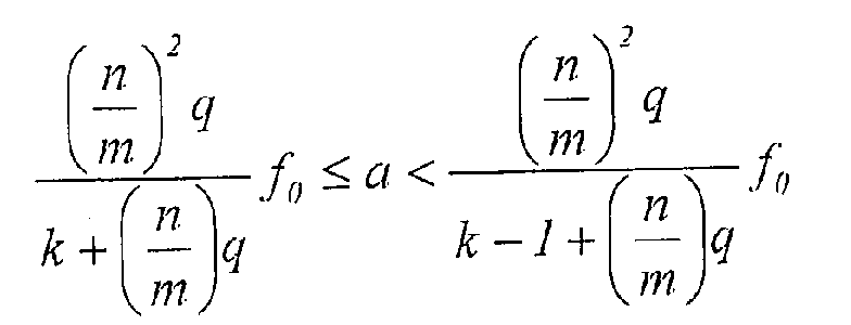
- Here, n/m is a value relating to the ratio between f0 and f1 , and if n/m is 1/100 and f0 is 10 (Gbit/s), for example, then f1 is approximately 100 (MHz), showing that the sampling frequency is such that one sampled point is obtained for every approximately 100 bits of the data signal. Furthermore, k is a value relating to the superposition period, indicating that sampled points are superposed in units of k. Furthermore, q is a value indicating how many bits of the data signal are reproduced when k sampled points are arranged in a time series. As an example, plotting examples of the points P1 to P8 each corresponding with a piece of sampled data are described below for a case where f1 = (n/m) - a, with reference to FIG. 9A to FIG. 9D. FIG. 9A is a diagram showing the waveform of a data signal (although only points P1 to P5 are shown in FIG. 9A), and FIG. 9B to FIG. 9D are diagrams showing plotting examples thereof. Furthermore, in this case the variables satisfy n/m = 1, k = 4 and q = 1.
- In the case above, the value of the offset frequency a (= ± (f1 -f0)) is within the range of (1/5) f0 ≤ a < (1/4) f0 . In other words, 1/4/f0 ≤ 1/f1 - 1/f0 < 1/3/f0 is satisfied, and Δt (= 1/f1 - 1/f0) is set to a value greater than 1/4 and less than 1/3 of one timeslot which is the reciprocal of f0 . The waveform within one timeslot is reproduced by arranging points P1 to P4 in order (FIG. 9B).
- In this example, point P5 is not plotted in a position following point P4, and is instead plotted after returning to time zero. Here, there are two possible superposition methods.
- (1) The first superposition method involves aligning the time position of point P5 with the time position of point P1, as shown in FIG. 9C. When the time position of point P5 is aligned to the time position of point P1, the second superposed waveform presents slight temporal deviation relative to the first waveform. In superposing the third and then fourth waveforms in the same manner, the degree of deviation increases gradually, and consequently the eye tends towards closing as the number of superposed waveforms increases. The only information required to realize this superposition is the value of n/m. Because the sampling clock can be set locally, k can be determined arbitrarily within the range of natural numbers, and the superposition period is determined according to k. k is a natural number, and it can be said that a larger value is preferable for the reproduction of a complicated waveform.
- (2) The second superposition method involves aligning the time position of point P5 to a multiple of 1/f0 , as shown in FIG. 9D. If the time position of point P5 is aligned to a multiple of 1/f0 , the second superposed waveform overlaps the first waveform. However, it is necessary to know the absolute value of f0 .
-
- First, the deviation occurring when the time position of point P5 is aligned to the same time position as point P1 in method (1) is estimated. If a = (1/4) f0 , then point P5 is aligned to point P1 at a period of 1/f0 , and consequently if superposition is performed in units of four points (or if superposition is performed based on a multiple of four), even if the superposition of waveforms is continued infinitely, a clean eye-diagram can be obtained. However, in this case, as is apparent from the equation above used to define the range of a, a deviates slightly from (1/4) f0 .
- Here, assuming that z is a real number which satisfies k - 1 < z ≤ k, thenand because in the current case n/m = 1 and q = 1, z is a real number which satisfies 3 < z < 4, and therefore a = {1 / (z + 1)} f0 . Performing the calculations based on these facts shows that in comparison with a case where a = (1/4) f0 , the size ΔT of the deviation which occurs when superposing waveforms is ΔT = (4 - z) / (zf0). In other words, if the period of the superposition is ik (where i is a natural number, in this example i = 1), then ΔT = q (k - z) i / (zf0). In other words, as the waveforms are superposed a second and a third time, and so on, each waveform deviates by an additional ΔT in the time domain. Once the total deviation equals half the size of a timeslot which is the reciprocal of f0 , the eye-diagram is completely closed, and as such this is the upper limit for deviation. If the number of sampled points to be measured at a time is deemed Nsamp, and the number of superposition is deemed j, then ikj ≤ Nsamp. Accordingly, if the total accumulated deviation is deemed Sum [ΔT], Sum [ΔT] is expressed as

- Because a condition for enabling eye opening evaluation is that this value is equal to or less than half of 1/f0 , if the number of sampled points is within a range which satisfies
- In other words, when the value of a is(where z is a real number which satisfies k - 1 < z ≤ k)

and Nsamp pieces of sampled data are displayed in the order of measurement at a time interval of dt = 1 / (zf0) in the time domain, then in the case where a signal eye-diagram is obtained and data signal waveform measurement and quality evaluation are performed by, deeming the time position of the first piece of the sampled data t = 0, displaying the plurality of pieces of the sampled data in a superposed manner by returning the time position to 0 each time t = p / f0 (where p is a natural number), if the number of superposition is deemed j (where j is a natural number), data signal quality evaluation can be performed for the entire number of pieces of the sampled data Nsamp, by satisfying pkj ≤ Nsamp. - To further expand on the above-described process, evaluation can be performed after repeating j times the process of acquiring Nsamp pieces of data and displaying an eye-diagram as described above, and then superposing j eye-diagrams based on the point where the eye opening is largest. Using this process, the effective number of sampled points used in the evaluation can be increased, thereby further reducing the indeterminacy of the evaluation.
Claims (18)
- A data signal quality evaluation method, comprising the steps of:after repeating N times (where N is a natural number) a process in which an input optical or electrical data signal with a bit rate of f0 (bit/s) is sampled using an optical or electrical sampling pulse train, which is generated independently of the data signal, and which has a repetition frequency f1 (Hz) which differs from the bit rate f0 (bit/s), a thus obtained optical or electrical sampled signal is converted into a piece of electrical digital data, and the piece of the electrical digital data is stored in a buffer,reading N pieces of the electrical digital data stored in the buffer at once or sequentially and performing electrical signal processing of the N pieces of the electrical digital data, to obtain a signal eye-diagram and to perform data signal waveform measurement and quality evaluation.
- A data signal quality evaluation method according to claim 1, wherein the repetition frequency f1 (Hz) of sampling satisfies f1 = (n/m) f0 ± a (where n and m are natural numbers), and a range of variable a is(where k and q are natural numbers).

- A data signal quality evaluation method according to claim 2, wherein when an accurate value for the bit rate f0 (bit/s) is unknown, the value of f1 is swept so that the repetition frequency f1 (Hz) of sampling satisfies f1 = (n/m) f0 ± a (where n and m are natural numbers) and (n/m) 2 q/{k + (n/m) q} f0 ≤ a < (n/m) 2 q/{k + (n/m) q - 1} f0 (where k is a natural number).
- A data signal quality evaluation method according to claim 2 or claim 3, wherein when the value of the variable a is expressed as(where z is a real number which satisfies k - 1 < z ≤ k) and pieces of sampled data are displayed in the order of measurement at a time interval of dt = 1/(zf0) in the time domain, the time positions of every ik piece (where i is a natural number) of the sampled data counting from the first piece of the sampled data are superposed and the pieces of the superposed sampled data are displayed, to obtain the signal eye-diagram and to perform the data signal waveform measurement and the quality evaluation, and

wherein when the number of times superposition is performed is j (where j is a natural number), ikj ≤ Nsamp is satisfied for the total number of pieces of the sampled data Nsamp. - A data signal quality evaluation method according claim 4, wherein the variables i and k are values which satisfy ikj ≤ Nsamp, and satisfy
- A data signal quality evaluation method according claim 5, wherein when an accurate value for the bit rate f0 (bit/s) is unknown, at least one of the value of k, the value of n/m and the value of q is swept so that the repetition frequency f1 (Hz) of sampling satisfies f1 = (n/m) f0 ± a (where n and m are natural numbers) and (n/m) 2q/{k + (n/m)q} f0 ≤ a < (n/m)2q/{k + (n/m) q - 1} f0 (where k is a natural number), and ikj ≤ Nsamp and ikj ≤ kz / {2q (k - z)} (where i, j, and Nsamp are natural numbers) are satisfied.
- A data signal quality evaluation method according to claim 2 or claim 3, wherein when the value of the variable a is expressed as(where z is a real number which satisfies k - 1 < z ≤ k)

and pieces of sampled data are displayed in the order of measurement at a time interval of dt = 1/(zf0) in the time domain, the time position of the first piece of the sampled data is deemed t = 0 and the pieces of the sampled data are displayed in a superposed manner by returning the time position to zero each time t = p/f0 (where p is a natural number), to obtain the signal eye-diagram and to perform the data signal waveform measurement and the quality evaluation, and
wherein when the number of times superposition is performed is j (where j is a natural number), pkj ≤ Nsamp is satisfied for the total number of pieces of the sampled data Nsamp. - A data signal quality evaluation method according to any one of claims 4, 5, 6, and 7, wherein by repeating a plurality of times a process of reading Nsamp pieces of the sampled data stored in the buffer at once or sequentially and performing electrical signal processing to obtain the signal eye-diagram, and superposing signal eye-diagrams so that the eye openings thereof match temporally, the total number of pieces of the sampled data which constitute the signal eye-diagrams is increased, and the data signal waveform measurement and the quality evaluation are performed.
- A data signal quality evaluation method according to any one of claims 2, 3, 4, 5, 6, 7, and 8, wherein either one of an amplitude histogram and a time histogram, determined from a sampled data distribution obtained by dividing an obtained eye-diagram in the intensity domain and the time domain, respectively, is used as a data signal quality parameter.
- A data signal quality evaluation apparatus, comprising:a sampling pulse train generation device which generates an optical or electrical sampling pulse train, independently of an input optical or electrical data signal with a bit rate of f0 (bit/s), and which has a repetition frequency f1 (Hz) which differs from the bit rate f0 (bit/s);a data signal sampling device which samples the data signal with the bit rate f0 (bit/s) in accordance with the sampling pulse train to obtain a sampled signal;a voltage retaining device which converts the sampled signal which is an optical or electrical sampled signal obtained by means of the data signal sampling device into a piece of electrical digital data, and stores a plurality of pieces of the electrical digital data;an electrical signal processing device which reads the plurality of pieces of the electrical digital data stored in the voltage retaining device at once or sequentially to obtain a signal eye-diagram and to evaluate optical data signal quality parameters; anda trigger signal generation device which applies triggers indicating the start/finish of data acquisition to the voltage retaining device, and applies triggers indicating the start/finish of data read to the electrical signal processing device.
- A data signal quality evaluation apparatus according to claim 10, wherein the repetition frequency f1 (Hz) of sampling satisfies f1 = (n/m) f0 ± a (where n and m are natural numbers), and a range of variable a is(where k and q are natural numbers).
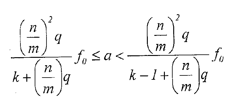
- A data signal quality evaluation apparatus according to claim 11, wherein the sampling pulse train generation device has a function which renders the repetition frequency f1 (Hz) of the generated sampling pulse train variable, and which when an accurate value for the bit rate f0 (bit/s) is unknown, sweeps the value of f1 so that f1 = (n/m) f0 ± a (where n and m are natural numbers) and
(n/m)2q/{k + (n/m)q} f0 ≤ a < (n/m)2q/{k + (n/m) q - 1} f0 (where k is a natural number) are satisfied. - A data signal quality evaluation apparatus according to claim 11 or claim 12, wherein when the value of the variable a is expressed as(where z is a real number which satisfies k - 1 < z ≤ k) and pieces of sampled data are displayed in the order of measurement at a time interval of dt = 1/(zf0) in the time domain, the time positions of every ik piece (where i is a natural number) of the sampled data counting from the first piece of the sampled data are superposed and the pieces of the superposed sampled data are displayed, to obtain the signal eye-diagram and to perform data signal waveform measurement and quality evaluation, and

wherein when the number of times superposition is performed is j (where j is a natural number), ikj ≤ Nsamp is satisfied for the total number of pieces of the sampled data Nsamp. - A data signal quality evaluation apparatus according to claim 13, wherein the variables i, k are values which satisfy ikj ≤ Nsamp, and satisfy
- A data signal quality evaluation apparatus according to claim 14, wherein when an accurate value for the bit rate f0 (bit/s) is unknown, the electrical signal processing device sweeps at least one of the value of k, the value of n/m and the value of q so that the repetition frequency f1 (Hz) of sampling satisfies f1 = (n/m) f0 ± a (where n and m are natural numbers) and (n/m) 2q/{k + (n/m)q} f0 ≤ a < (n/m) 2q/{k + (n/m) q - 1} f0 (where k is a natural number), and ikj ≤ Nsamp and ikj ≤ kz / {2q (k - z)} (where i, j, and Nsamp are natural numbers) are satisfied.
- A data signal quality evaluation apparatus according to claim 11 or claim 12, wherein when the value of the variable a is expressed as(where z is a real number which satisfies k - 1 < z ≤ k)

and pieces of sampled data are displayed in the order of measurement at a time interval of dt = 1/(zf0) in the time domain, the time position of the first piece of the sampled data is deemed t = 0 and the pieces of the sampled data are displayed in a superposed manner by returning the time position to zero each time t = p/f0 (where p is a natural number), to obtain a signal eye-diagram and to perform data signal waveform measurement and quality evaluation, and
wherein when the number of times superposition is performed is j (where j is a natural number), pkj ≤ Nsamp is satisfied for the total number of pieces of the sampled data Nsamp. - A data signal quality evaluation apparatus according to any one of claims 13, 14, 15 and 16, wherein the electrical signal processing device repeats a plurality of times a process of reading the Nsamp pieces of the sampled data stored in the voltage retaining device at once or sequentially and obtaining a signal eye-diagram, and
wherein the data signal quality evaluation apparatus further comprises an eye opening evaluation section which evaluates the eye-opening of signal eye-diagrams, and the total number of pieces of the sampled data which constitute the signal eye-diagrams for the data signal waveform measurement and the quality evaluation is increased by superposing the signal eye-diagrams so that the eye openings thereof match temporally. - A data signal quality evaluation apparatus according to any one of claims 11, 12, 13, 14, 15, 16, and 17, wherein
the electrical signal processing device comprises at least one of an amplitude histogram evaluation section which determines an amplitude histogram as a data signal quality parameter and a time histogram evaluation section which determines a time histogram as a data signal quality parameter, and
the amplitude histogram and the time histogram are determined from a sampled data distribution obtained by dividing a signal eye-diagram in the amplitude domain and the time domain, respectively.
Applications Claiming Priority (4)
| Application Number | Priority Date | Filing Date | Title |
|---|---|---|---|
| JP2002139006 | 2002-05-14 | ||
| JP2002139006 | 2002-05-14 | ||
| JP2003118299 | 2003-04-23 | ||
| JP2003118299A JP3987001B2 (en) | 2002-05-14 | 2003-04-23 | Data signal quality evaluation method and apparatus by high speed sampling |
Publications (3)
| Publication Number | Publication Date |
|---|---|
| EP1363423A2 true EP1363423A2 (en) | 2003-11-19 |
| EP1363423A3 EP1363423A3 (en) | 2006-10-04 |
| EP1363423B1 EP1363423B1 (en) | 2011-07-06 |
Family
ID=29272397
Family Applications (1)
| Application Number | Title | Priority Date | Filing Date |
|---|---|---|---|
| EP03101315A Expired - Lifetime EP1363423B1 (en) | 2002-05-14 | 2003-05-12 | Data signal quality evaluation method and apparatus using high speed sampling |
Country Status (3)
| Country | Link |
|---|---|
| US (1) | US7190752B2 (en) |
| EP (1) | EP1363423B1 (en) |
| JP (1) | JP3987001B2 (en) |
Cited By (1)
| Publication number | Priority date | Publication date | Assignee | Title |
|---|---|---|---|---|
| US7684697B2 (en) | 2004-06-03 | 2010-03-23 | Nippon Telegraph And Telephone Corporation | Optical signal quality monitoring circuit and optical signal quality monitoring method |
Families Citing this family (18)
| Publication number | Priority date | Publication date | Assignee | Title |
|---|---|---|---|---|
| US20060039513A1 (en) * | 2004-08-17 | 2006-02-23 | Ruey-Bin Sheen | Clock and data recovery systems and methods |
| WO2006028695A2 (en) * | 2004-09-07 | 2006-03-16 | Magiq Technologies, Inc. | Systems and methods for multiplexing qkd channels |
| US8625986B2 (en) * | 2006-09-27 | 2014-01-07 | Tti Inventions A Llc | Methods and systems for optical performance monitoring |
| JP4915196B2 (en) * | 2006-09-28 | 2012-04-11 | 沖電気工業株式会社 | Optical signal quality monitoring device |
| US7462956B2 (en) * | 2007-01-11 | 2008-12-09 | Northrop Grumman Space & Mission Systems Corp. | High efficiency NLTL comb generator using time domain waveform synthesis technique |
| JP4552977B2 (en) * | 2007-07-13 | 2010-09-29 | 沖電気工業株式会社 | Optical signal quality monitoring device |
| JP5334551B2 (en) * | 2008-12-05 | 2013-11-06 | アンリツ株式会社 | Sampling waveform measuring device and signal quality monitor |
| JP5377118B2 (en) * | 2009-07-01 | 2013-12-25 | 新光電気工業株式会社 | Sampling point detection circuit, transmission system, pre-emphasis intensity adjustment method, logic analyzer, and evaluation method for evaluating transmission path |
| CN101986580B (en) * | 2009-07-29 | 2013-08-14 | 澜起科技(上海)有限公司 | Method and device for measuring and compensating parameters of receiver |
| CN102045120B (en) * | 2010-10-29 | 2013-11-13 | 成都九洲电子信息系统股份有限公司 | Vibration signal identification method for optical fiber perimeter system |
| US8885695B1 (en) | 2013-06-26 | 2014-11-11 | Global Unichip Corporation | Receiver circuit |
| US9071477B2 (en) | 2013-10-09 | 2015-06-30 | Global Unichip Corporation | Method and associated processing module for interconnection system |
| CN104407190B (en) | 2014-11-26 | 2017-02-01 | 电子科技大学 | Fully-digital random sampling method |
| JP6901238B2 (en) * | 2015-06-29 | 2021-07-14 | ローム株式会社 | Switching regulator and integrated circuit package |
| US10637581B2 (en) * | 2018-03-20 | 2020-04-28 | Lumentum Operations Llc | Dynamic range for a heterodyne optical channel monitor |
| JP7449785B2 (en) * | 2020-06-17 | 2024-03-14 | 日立Astemo株式会社 | Electronic control device, determination method |
| EP4066749B1 (en) * | 2021-02-05 | 2024-08-14 | Shenzhen Institutes of Advanced Technology Chinese Academy of Sciences | Soft apparatus for opening eyelids and method therefor |
| US20250015886A1 (en) * | 2021-11-30 | 2025-01-09 | Telefonaktiebolaget Lm Ericsson (Publ) | Signal quality monitoring method |
Citations (4)
| Publication number | Priority date | Publication date | Assignee | Title |
|---|---|---|---|---|
| JP2677372B2 (en) | 1988-02-26 | 1997-11-17 | 日本電信電話株式会社 | Optical sampling oscilloscope |
| EP0884868A2 (en) | 1997-06-09 | 1998-12-16 | Nortel Networks Corporation | Measurement of the eye-opening of optical signals by optical sampling |
| EP0920150A2 (en) | 1997-12-01 | 1999-06-02 | Nippon Telegraph And Telephone Corporation | System for monitoring quality of optical signals having different bit rates |
| JP3239925B2 (en) | 1995-12-08 | 2001-12-17 | 日本電信電話株式会社 | Optical sampling optical waveform measurement device |
Family Cites Families (8)
| Publication number | Priority date | Publication date | Assignee | Title |
|---|---|---|---|---|
| GB2319915B (en) * | 1996-11-29 | 2001-01-24 | Lsi Logic Corp | Analogue to digital converter system |
| US4376309A (en) | 1981-05-29 | 1983-03-08 | Bell Telephone Laboratories, Incorporated | Method and apparatus for signal-eye tracking in digital transmission systems |
| DE3783915T2 (en) | 1987-10-19 | 1993-08-19 | Ibm | PREDICTIVE CLOCK RECOVERY CIRCUIT. |
| JPH05142095A (en) | 1991-11-20 | 1993-06-08 | Nec Corp | Device for judging quality of light signal eye pattern waveform |
| JPH0810851B2 (en) | 1993-01-11 | 1996-01-31 | 日本電気株式会社 | Waveform identification device |
| AU2001257341A1 (en) * | 2000-04-26 | 2001-11-07 | Optovation Corporation | Ac performance monitor with no clock recovery |
| US6593871B1 (en) * | 2000-08-31 | 2003-07-15 | Dalsa, Inc. | Automatic A/D convert positioning circuit and method |
| US6587530B1 (en) * | 2000-10-05 | 2003-07-01 | International Business Machines Corporation | Method and apparatus for signal integrity verification |
-
2003
- 2003-04-23 JP JP2003118299A patent/JP3987001B2/en not_active Expired - Lifetime
- 2003-05-09 US US10/434,840 patent/US7190752B2/en not_active Expired - Lifetime
- 2003-05-12 EP EP03101315A patent/EP1363423B1/en not_active Expired - Lifetime
Patent Citations (4)
| Publication number | Priority date | Publication date | Assignee | Title |
|---|---|---|---|---|
| JP2677372B2 (en) | 1988-02-26 | 1997-11-17 | 日本電信電話株式会社 | Optical sampling oscilloscope |
| JP3239925B2 (en) | 1995-12-08 | 2001-12-17 | 日本電信電話株式会社 | Optical sampling optical waveform measurement device |
| EP0884868A2 (en) | 1997-06-09 | 1998-12-16 | Nortel Networks Corporation | Measurement of the eye-opening of optical signals by optical sampling |
| EP0920150A2 (en) | 1997-12-01 | 1999-06-02 | Nippon Telegraph And Telephone Corporation | System for monitoring quality of optical signals having different bit rates |
Non-Patent Citations (4)
| Title |
|---|
| H. TAKARA; S. KAWANISHI; A. YOKOO; S. TOMARU; T. KITOH; M. SARUWATARI, ELECTRONICS LETTERS, vol. 32, no. 24, 21 November 1996 (1996-11-21), pages 2256 - 2258 |
| I. SHAKE; H. TAKARA; S. KAWANISHI; Y. YAMABAYASHI: "Optical signal quality monitoring method based on optical sampling", ELECTRONICS LETTERS, vol. 34, no. 22, 29 October 1998 (1998-10-29), pages 2152 - 2154, XP006010507, DOI: doi:10.1049/el:19981465 |
| JOHN D. LENK; ENGLEWOOD CLIFFS, N. J.: "Handbook of ELECTRONIC TEST EQUIPMENT", 1971, PRENTICE-HALL, INC., pages: 184 - 189 |
| SEDKI M. RIAD: "Modeling of the HP-1430A Feedthrough Wide-Band (28-ps) Sampling Head", IEEE TRANSACTIONS ON INSTRUMENTATION AND MEASUREMENT, vol. IM-31, no. 2, June 1982 (1982-06-01), pages 110 - 115, XP001459070 |
Cited By (3)
| Publication number | Priority date | Publication date | Assignee | Title |
|---|---|---|---|---|
| US7684697B2 (en) | 2004-06-03 | 2010-03-23 | Nippon Telegraph And Telephone Corporation | Optical signal quality monitoring circuit and optical signal quality monitoring method |
| CN103312410A (en) * | 2004-06-03 | 2013-09-18 | 日本电信电话株式会社 | Optical signal quality monitoring circuit and optical signal quality monitoring method |
| CN103312410B (en) * | 2004-06-03 | 2016-05-04 | 日本电信电话株式会社 | Optical signal quality monitoring circuit and optical signal quality monitoring method |
Also Published As
| Publication number | Publication date |
|---|---|
| JP2004048688A (en) | 2004-02-12 |
| JP3987001B2 (en) | 2007-10-03 |
| US7190752B2 (en) | 2007-03-13 |
| US20040005000A1 (en) | 2004-01-08 |
| EP1363423B1 (en) | 2011-07-06 |
| EP1363423A3 (en) | 2006-10-04 |
Similar Documents
| Publication | Publication Date | Title |
|---|---|---|
| EP1363423B1 (en) | Data signal quality evaluation method and apparatus using high speed sampling | |
| Westlund et al. | Software-synchronized all-optical sampling for fiber communication systems | |
| DE69834999T2 (en) | Quality monitoring system of optical signals with different bit rates | |
| Fontaine et al. | Real-time full-field arbitrary optical waveform measurement | |
| US8686712B2 (en) | Time stretch enhanced recording scope | |
| CN110832295B (en) | Real-time Optical Spectroscopy-Time Analyzers and Methods | |
| Dorrer | High-speed measurements for optical telecommunication systems | |
| US6751385B2 (en) | Method and device for measuring the waveform of an optical signal | |
| Jungerman et al. | 1-THz bandwidth C-and L-band optical sampling with a bit rate agile timebase | |
| Yamada et al. | 640-Gb/s OTDM signal measurement with high-resolution optical sampling system using wavelength-tunable soliton pulses | |
| US5880837A (en) | Eye measurement of optical signals by optical sampling | |
| US5870211A (en) | Error rate measurement system for high speed optical pulse signals | |
| CA2424276C (en) | Method and apparatus for signal integrity verification | |
| CN113834574B (en) | Ultrashort optical pulse measurement system and method | |
| EP0884868B1 (en) | Measurement of the eye-opening of optical signals by optical sampling | |
| EP1669730A2 (en) | Heterodyne-based optical spectrum analysis using data clock sampling | |
| Bogoni et al. | New optical sampler based on TOAD and data postprocessing for subpicosecond pulse resolution | |
| JP5366139B2 (en) | Optical signal waveform measuring device | |
| Reid et al. | Linear spectrograms using electrooptic modulators | |
| Otani et al. | Novel optical sampling oscilloscope using envelope detection triggering method | |
| Set et al. | Asynchronous Nonlinear Optical Sampling with Parallelized Signal Reconstruction | |
| CN115165106A (en) | Ultrafast spectral intensity and phase information measuring method and device | |
| JP3286151B2 (en) | Optical sampling device | |
| Benkler et al. | Word-synchronous optical sampling of periodically repeated OTDM data words for true waveform visualization | |
| Mori et al. | A simple synchronization method for optical sampling eye monitor |
Legal Events
| Date | Code | Title | Description |
|---|---|---|---|
| PUAI | Public reference made under article 153(3) epc to a published international application that has entered the european phase |
Free format text: ORIGINAL CODE: 0009012 |
|
| AK | Designated contracting states |
Kind code of ref document: A2 Designated state(s): AT BE BG CH CY CZ DE DK EE ES FI FR GB GR HU IE IT LI LU MC NL PT RO SE SI SK TR |
|
| AX | Request for extension of the european patent |
Extension state: AL LT LV MK |
|
| PUAL | Search report despatched |
Free format text: ORIGINAL CODE: 0009013 |
|
| AK | Designated contracting states |
Kind code of ref document: A3 Designated state(s): AT BE BG CH CY CZ DE DK EE ES FI FR GB GR HU IE IT LI LU MC NL PT RO SE SI SK TR |
|
| AX | Request for extension of the european patent |
Extension state: AL LT LV MK |
|
| RIC1 | Information provided on ipc code assigned before grant |
Ipc: H04L 1/20 20060101ALI20060831BHEP Ipc: H04L 1/24 20060101AFI20030913BHEP |
|
| 17P | Request for examination filed |
Effective date: 20070323 |
|
| AKX | Designation fees paid |
Designated state(s): DE FR GB |
|
| 17Q | First examination report despatched |
Effective date: 20100707 |
|
| GRAP | Despatch of communication of intention to grant a patent |
Free format text: ORIGINAL CODE: EPIDOSNIGR1 |
|
| GRAS | Grant fee paid |
Free format text: ORIGINAL CODE: EPIDOSNIGR3 |
|
| GRAA | (expected) grant |
Free format text: ORIGINAL CODE: 0009210 |
|
| AK | Designated contracting states |
Kind code of ref document: B1 Designated state(s): DE FR GB |
|
| REG | Reference to a national code |
Ref country code: GB Ref legal event code: FG4D |
|
| REG | Reference to a national code |
Ref country code: DE Ref legal event code: R096 Ref document number: 60337612 Country of ref document: DE Effective date: 20110908 |
|
| PLBE | No opposition filed within time limit |
Free format text: ORIGINAL CODE: 0009261 |
|
| STAA | Information on the status of an ep patent application or granted ep patent |
Free format text: STATUS: NO OPPOSITION FILED WITHIN TIME LIMIT |
|
| 26N | No opposition filed |
Effective date: 20120411 |
|
| REG | Reference to a national code |
Ref country code: DE Ref legal event code: R097 Ref document number: 60337612 Country of ref document: DE Effective date: 20120411 |
|
| REG | Reference to a national code |
Ref country code: FR Ref legal event code: PLFP Year of fee payment: 14 |
|
| REG | Reference to a national code |
Ref country code: FR Ref legal event code: PLFP Year of fee payment: 15 |
|
| REG | Reference to a national code |
Ref country code: FR Ref legal event code: PLFP Year of fee payment: 16 |
|
| PGFP | Annual fee paid to national office [announced via postgrant information from national office to epo] |
Ref country code: GB Payment date: 20220519 Year of fee payment: 20 Ref country code: FR Payment date: 20220523 Year of fee payment: 20 Ref country code: DE Payment date: 20220519 Year of fee payment: 20 |
|
| REG | Reference to a national code |
Ref country code: DE Ref legal event code: R071 Ref document number: 60337612 Country of ref document: DE |
|
| REG | Reference to a national code |
Ref country code: GB Ref legal event code: PE20 Expiry date: 20230511 |
|
| PG25 | Lapsed in a contracting state [announced via postgrant information from national office to epo] |
Ref country code: GB Free format text: LAPSE BECAUSE OF EXPIRATION OF PROTECTION Effective date: 20230511 |