EP1363158A1 - Waveguide type liquid crystal optical switch - Google Patents
Waveguide type liquid crystal optical switch Download PDFInfo
- Publication number
- EP1363158A1 EP1363158A1 EP03011012A EP03011012A EP1363158A1 EP 1363158 A1 EP1363158 A1 EP 1363158A1 EP 03011012 A EP03011012 A EP 03011012A EP 03011012 A EP03011012 A EP 03011012A EP 1363158 A1 EP1363158 A1 EP 1363158A1
- Authority
- EP
- European Patent Office
- Prior art keywords
- core
- liquid crystal
- optical switch
- type liquid
- waveguide type
- Prior art date
- Legal status (The legal status is an assumption and is not a legal conclusion. Google has not performed a legal analysis and makes no representation as to the accuracy of the status listed.)
- Withdrawn
Links
- 230000003287 optical effect Effects 0.000 title claims abstract description 206
- 239000004973 liquid crystal related substance Substances 0.000 title claims abstract description 106
- 238000005253 cladding Methods 0.000 claims abstract description 29
- 239000004988 Nematic liquid crystal Substances 0.000 claims abstract description 7
- 230000008878 coupling Effects 0.000 claims description 26
- 238000010168 coupling process Methods 0.000 claims description 26
- 238000005859 coupling reaction Methods 0.000 claims description 26
- 239000013307 optical fiber Substances 0.000 claims description 3
- 239000000758 substrate Substances 0.000 description 26
- 239000000463 material Substances 0.000 description 14
- 238000004891 communication Methods 0.000 description 6
- 238000010276 construction Methods 0.000 description 5
- 230000001419 dependent effect Effects 0.000 description 4
- 230000000694 effects Effects 0.000 description 4
- XOLBLPGZBRYERU-UHFFFAOYSA-N tin dioxide Chemical compound O=[Sn]=O XOLBLPGZBRYERU-UHFFFAOYSA-N 0.000 description 4
- 230000008033 biological extinction Effects 0.000 description 3
- 230000005540 biological transmission Effects 0.000 description 3
- 238000003780 insertion Methods 0.000 description 3
- 230000037431 insertion Effects 0.000 description 3
- 238000005259 measurement Methods 0.000 description 3
- DTPSXFMGMQOVTG-UHFFFAOYSA-N n-[4-[3-(2-aminocyclopropyl)phenoxy]-1-(benzylamino)-1-oxobutan-2-yl]benzamide Chemical compound NC1CC1C1=CC=CC(OCCC(NC(=O)C=2C=CC=CC=2)C(=O)NCC=2C=CC=CC=2)=C1 DTPSXFMGMQOVTG-UHFFFAOYSA-N 0.000 description 3
- RYGMFSIKBFXOCR-UHFFFAOYSA-N Copper Chemical compound [Cu] RYGMFSIKBFXOCR-UHFFFAOYSA-N 0.000 description 2
- 230000005679 Peltier effect Effects 0.000 description 2
- VYPSYNLAJGMNEJ-UHFFFAOYSA-N Silicium dioxide Chemical compound O=[Si]=O VYPSYNLAJGMNEJ-UHFFFAOYSA-N 0.000 description 2
- 229910052782 aluminium Inorganic materials 0.000 description 2
- XAGFODPZIPBFFR-UHFFFAOYSA-N aluminium Chemical compound [Al] XAGFODPZIPBFFR-UHFFFAOYSA-N 0.000 description 2
- 239000004020 conductor Substances 0.000 description 2
- 229910052802 copper Inorganic materials 0.000 description 2
- 239000010949 copper Substances 0.000 description 2
- 230000005684 electric field Effects 0.000 description 2
- 239000007772 electrode material Substances 0.000 description 2
- PCHJSUWPFVWCPO-UHFFFAOYSA-N gold Chemical compound [Au] PCHJSUWPFVWCPO-UHFFFAOYSA-N 0.000 description 2
- 229910052737 gold Inorganic materials 0.000 description 2
- 239000010931 gold Substances 0.000 description 2
- 230000031700 light absorption Effects 0.000 description 2
- 239000007769 metal material Substances 0.000 description 2
- FURZYCFZFBYJBT-UHFFFAOYSA-N 4-(4-pentylcyclohexyl)benzonitrile Chemical compound C1CC(CCCCC)CCC1C1=CC=C(C#N)C=C1 FURZYCFZFBYJBT-UHFFFAOYSA-N 0.000 description 1
- 229910003327 LiNbO3 Inorganic materials 0.000 description 1
- 239000004952 Polyamide Substances 0.000 description 1
- 229910003910 SiCl4 Inorganic materials 0.000 description 1
- 229910003074 TiCl4 Inorganic materials 0.000 description 1
- 239000000853 adhesive Substances 0.000 description 1
- 230000002411 adverse Effects 0.000 description 1
- 230000002238 attenuated effect Effects 0.000 description 1
- 229910052681 coesite Inorganic materials 0.000 description 1
- 229910052906 cristobalite Inorganic materials 0.000 description 1
- 239000013078 crystal Substances 0.000 description 1
- 230000007547 defect Effects 0.000 description 1
- 239000000835 fiber Substances 0.000 description 1
- 239000011521 glass Substances 0.000 description 1
- 238000002347 injection Methods 0.000 description 1
- 239000007924 injection Substances 0.000 description 1
- 238000004519 manufacturing process Methods 0.000 description 1
- 229920002647 polyamide Polymers 0.000 description 1
- 239000004065 semiconductor Substances 0.000 description 1
- 239000000377 silicon dioxide Substances 0.000 description 1
- FDNAPBUWERUEDA-UHFFFAOYSA-N silicon tetrachloride Chemical compound Cl[Si](Cl)(Cl)Cl FDNAPBUWERUEDA-UHFFFAOYSA-N 0.000 description 1
- 229910052682 stishovite Inorganic materials 0.000 description 1
- GWEVSGVZZGPLCZ-UHFFFAOYSA-N titanium dioxide Inorganic materials O=[Ti]=O GWEVSGVZZGPLCZ-UHFFFAOYSA-N 0.000 description 1
- 229910052905 tridymite Inorganic materials 0.000 description 1
Images



Classifications
-
- G—PHYSICS
- G02—OPTICS
- G02F—OPTICAL DEVICES OR ARRANGEMENTS FOR THE CONTROL OF LIGHT BY MODIFICATION OF THE OPTICAL PROPERTIES OF THE MEDIA OF THE ELEMENTS INVOLVED THEREIN; NON-LINEAR OPTICS; FREQUENCY-CHANGING OF LIGHT; OPTICAL LOGIC ELEMENTS; OPTICAL ANALOGUE/DIGITAL CONVERTERS
- G02F1/00—Devices or arrangements for the control of the intensity, colour, phase, polarisation or direction of light arriving from an independent light source, e.g. switching, gating or modulating; Non-linear optics
- G02F1/01—Devices or arrangements for the control of the intensity, colour, phase, polarisation or direction of light arriving from an independent light source, e.g. switching, gating or modulating; Non-linear optics for the control of the intensity, phase, polarisation or colour
- G02F1/13—Devices or arrangements for the control of the intensity, colour, phase, polarisation or direction of light arriving from an independent light source, e.g. switching, gating or modulating; Non-linear optics for the control of the intensity, phase, polarisation or colour based on liquid crystals, e.g. single liquid crystal display cells
- G02F1/1326—Liquid crystal optical waveguides or liquid crystal cells specially adapted for gating or modulating between optical waveguides
-
- G—PHYSICS
- G02—OPTICS
- G02F—OPTICAL DEVICES OR ARRANGEMENTS FOR THE CONTROL OF LIGHT BY MODIFICATION OF THE OPTICAL PROPERTIES OF THE MEDIA OF THE ELEMENTS INVOLVED THEREIN; NON-LINEAR OPTICS; FREQUENCY-CHANGING OF LIGHT; OPTICAL LOGIC ELEMENTS; OPTICAL ANALOGUE/DIGITAL CONVERTERS
- G02F1/00—Devices or arrangements for the control of the intensity, colour, phase, polarisation or direction of light arriving from an independent light source, e.g. switching, gating or modulating; Non-linear optics
- G02F1/29—Devices or arrangements for the control of the intensity, colour, phase, polarisation or direction of light arriving from an independent light source, e.g. switching, gating or modulating; Non-linear optics for the control of the position or the direction of light beams, i.e. deflection
- G02F1/31—Digital deflection, i.e. optical switching
- G02F1/313—Digital deflection, i.e. optical switching in an optical waveguide structure
- G02F1/3132—Digital deflection, i.e. optical switching in an optical waveguide structure of directional coupler type
-
- G—PHYSICS
- G02—OPTICS
- G02F—OPTICAL DEVICES OR ARRANGEMENTS FOR THE CONTROL OF LIGHT BY MODIFICATION OF THE OPTICAL PROPERTIES OF THE MEDIA OF THE ELEMENTS INVOLVED THEREIN; NON-LINEAR OPTICS; FREQUENCY-CHANGING OF LIGHT; OPTICAL LOGIC ELEMENTS; OPTICAL ANALOGUE/DIGITAL CONVERTERS
- G02F1/00—Devices or arrangements for the control of the intensity, colour, phase, polarisation or direction of light arriving from an independent light source, e.g. switching, gating or modulating; Non-linear optics
- G02F1/29—Devices or arrangements for the control of the intensity, colour, phase, polarisation or direction of light arriving from an independent light source, e.g. switching, gating or modulating; Non-linear optics for the control of the position or the direction of light beams, i.e. deflection
- G02F1/31—Digital deflection, i.e. optical switching
- G02F1/313—Digital deflection, i.e. optical switching in an optical waveguide structure
Definitions
- the present invention is related to an optical switch employed in, for instance, optical communication systems. More specifically, the present invention is directed to a waveguide type liquid crystal optical switch for controlling switching operations of optical paths between waveguides by way of liquid crystal.
- optical communications correspond to transmission systems by employing optical fibers.
- various sorts of optical components known as fiber type optical couplers, optical wavelength division multiplexers/demultiplexers, optical waveguide type branching/combining devices, and optical switches have been developed.
- optical switches may have switching functions of optical paths, and thus, maybecome important as switching devices for optical communications.
- various sorts of optical switches utilized in optical communications are known in this technical field.
- optical switches since such an optical switching system that while optical waveguides are used, optical transmission paths are switched by utilizing various sorts of physical phenomena is not equipped with any mechanical movable portion, this optical switching system has merits of high reliability and highspeed operations.
- various optical switches are known.
- optical switches using dielectric crystal waveguides such as LiNbO 3 having either the electrooptic effect or the acostooptic effect
- optical switches using semiconductor waveguides, while carrier injection is utilized
- optical switches using silica-system waveguides, while the thermooptic effect is utilized.
- liquid crystal may have the electrooptic effect under which refractive indexes are changed by applying electric field to the liquid crystal, in view of a broad sense .
- liquid crystal may have various characteristics, namely, liquid crystal may be driven under low voltages, may have high reliability (actually realized as display devices), may have high productivity, and may be manufactured in low cost.
- optical wavelength type liquid crystal switches for example, Japanese Unexamined Patent Publication No.
- H05-165068A describes such a waveguide type liquid crystal optical switch constituted in such a manner that two parallel single-mode optical core patterns are formed on the lower cladding and are equipped with the coupling portions, the partial portions of which are located in close proximity to each other; and furthermore, the lower electrode is formed on the lower cladding of the coupling portions, the coupling portions are filled with the orientated liquid crystal; and the coupling portions are sealed by the glass plate having the upper electrode.
- the lower electrode is located very close to the coupling portion of the waveguide, so that the loss causedbythis lower electrodebecomes very large.
- this waveguide type liquid crystal optical switch has such a construction that only one pair of upper/lower electrodes are limitedly arranged, this optical switch has another problem that the polarized-wave dependent characteristics thereof are strongly emphasized.
- the present invention has been made to solve these problems of the conventional optical switch, and therefore, has an object to provide a waveguide type liquid crystal optical switch capable of improving crosstalk performance and insertion loss and further having no polarized-wave dependent characteristic in addition to the merits specific to such a waveguide type liquid crystal optical switch, namely, low cost, high reliability, and low power consumption.
- a waveguide type liquid crystal optical switch is featured by that in an optical switch equipped with an optical waveguide having one pair of a first core and a second core located in proximity to the first core, for entering light into any one of the first core and the second core and for switching an optical path of the entered light between both the first core and the second core, such a waveguide type liquid crystal optical switch is comprised of: a third core provided apart from both the first core and the second core in such a manner that the third core covers a space sandwiched by both the first core and the second core, into which nematic liquid crystal orientated by an orientation film along a predetermined direction is filled; a first electrode of the third core, arranged on the opposite side with respect to both the first core and the second core in such a manner that a gap portion between the first core and the second core is covered by the first electrode; a second electrode and a third electrode, which are arranged to constitute a pair by sandwiching the first electrode, and cause liquid crystal
- Fig. 1 is a plan view for indicating a waveguide type liquid crystal optical switch 10 according to an embodiment of the present invention, as viewed from a core side thereof (namely, lower side of Fig. 2).
- Fig. 2 is a sectional view of this waveguide type liquid crystal optical switch 10, taken along a line A-A of Fig. 1.
- the waveguide type liquid crystal optical switch 10 is subdivided into two substrates, namely, an upper substrate 8A and a lower substrate 8B. Both a first core 1A and a second core 1B are embedded at a predetermined depth position in this lower substrate 8B from a surface of the lower substrate 8B along an axial line direction of this lower substrate 8B.
- both the first core 1A and the second core 1B are located in parallel to each other. Intervals between the first core 1A and the second core 1B are gradually widened toward edges of both end portions. This approached parallel portion may form a so-called "optical directional coupler.”
- the upper substrate 8A and the lower substrate 8B are manufactured by such a material having a refractive index lower than that of a material used to manufacture the first core 1A and the second core 1B.
- This material of both the upper substrate 8A and the lower substrate 8B is selected to be, for example, a material of (SiO 2 - TiO 2 ) having a refractive index of 1.523.
- the material of both the first core 1A and the second core 1B is selected to be, for instance, a material of (SiCl 4 - TiCl 4 ) having a refractive index of 1.530.
- a concave portion having a rectangular shape as viewed in a sectional plane is formed in a stripe form on a surface of the upper substrate 8A opposing the lower substrate 8B so that that this concave portion covers a space which is sandwiched by both the first core 1A and the second core 1B.
- An orientation film 7A is formed on a bottom portion of this concave portion, and nematic liquid crystal is filled on this orientation film 7A.
- orientation film 7B is provided on the lower substrate 8B in such a manner that an entire surface of this lower substrate 8B is covered by this orientation film 7B, the nematic liquid crystal is sealed by joining the upper substrate 8A to the lower substrate 8B by way of a properly-selected optical adhesive agent 11 to form an integral body, so that a third core 4 is formed.
- the sort of nematic liquid crystal which constitutes the third core 4 there is no limitation as to the sort of nematic liquid crystal which constitutes the third core 4, and therefore, for example, 4- (4-pentylcyclohexyl) cyanobenzene and the like maybe used.
- the materials of both the orientation film 7A and the orientation film 7B may be selected from any materials known in the technical field. For example, a polyamide film and the like, which have been rubbing-processed, may be used.
- a first electrode 6B is provided in the upper substrate 8A just above the third core 4 in such a manner that a gap between the first core 1A and the second core 1B is covered by this first electrode 6B. Furthermore, both a second electrode 6A and a third electrode 6C are formed on both sides of the first electrode 6B. The first electrode 6B, the second electrode 6A, and the third electrode 6C are controllable in an independent manner. Also, both the second electrode 6A and the third electrode 6C may define that the orientation direction of the liquid crystal molecules is intersected perpendicular to the orientation direction of the orientation films 7A and 7B.
- the electrode material metal materials such as gold, copper, and aluminum may be used in addition to transparent electric conductive materials such as SnO 2 and ITO or the like.
- the optical path can be switched (namely, switching operation) between the first core 1A and the second core 1B by adjusting voltages applied to the first to third electrodes 6A to 6C so as to control the orientation of the liquid crystal molecules of the third core 4 .
- an optical signal 5A and another optical signal 5B may be penetrated from respective cores provided on the light incident side to the third core 4, and may be furthermore transferred to other cores.
- the optical signals which have been transferred to other cores may be again penetrated through the third core 4, and furthermore, may be transferred to the respective cores provided on the light incident side.
- the above-described switching modes become reversed in the case that the nematic liquid crystal used in the third core 4 represents the positive change in the refractive indexes, and represents the negative change in the refractive indexes.
- the operation mode of the waveguide type liquid crystal optical switch may be preferably set to either an A-mode coupling or B-mode coupling. Any one of these A-mode and B-mode couplings indicates such a case under the above-described ON state.
- both the first core 1A and the second core 1B are set as follows: At respective intermediate positions of these first and second cores 1A and 1B along optical axial directions thereof, both light intensity of the core into which light is entered within the first and second cores (for example, first core 1A) , and light intensity of the third core 4 may become minimal values, and also, light intensity of the core into which the light is not entered within the first and second cores (for instance, second core 1B) may become a maximum value.
- a portion of the light entered into the first core 1A is transferred via the third core 4 to the second core 1B, and thereafter, is similarly returned via the third core 4 to the first core 1A.
- the respective cores must be designed in such a manner that a time period during which the incident light is transferred from the first core 1A to the second core 1B is made coincident with another time period during which the incident light is transferred via the third core 4 to either the first core 1A or the second core 1B.
- Fig. 5A shows such a measurement result that while a waveguide type liquid crystal optical switch manufactured based upon the below-mentioned design ideas was employed, changes in light intensity of the respective cores were actually measured. It should also be noted that dimensional places are illustrated in Figs. 6A and 6B.
- W 8 ⁇ m
- D 5 ⁇ m
- G LC 1.5 ⁇ m
- H LC 1.6 ⁇ m
- W LC 8 ⁇ m
- L LC 2.97 ⁇ m.
- both the first core 1A and the second core 1B are set as follows: At respective intermediate positions of these first and second cores 1A and 1B along optical axial directions thereof, light intensity of the core into which light is entered within the first and second cores (for example, first core 1A) may become a minimal value, and also, both light intensity of the core into which the light is not entered within the first and second cores (for instance, second core 1B) and light intensity of the third core 4 may become maximum values.
- a designing example capable of realizing the B-mode coupling is shown in the below-mentioned description (dimensional places as illustrated in Figs. 6A and 6B) .
- This B-mode coupling has such a feature that both the first core 1A and the second core 1B are formed at such positions within the lower substrate 8B, which are located deeper than those of the A-mode coupling.
- Fig. 5B shows such a result that while a waveguide type liquid crystal optical switch manufactured based upon the below-mentioned design ideas was employed, changes in light intensity of the respective cores were actually measured.
- W 8 ⁇ m
- D 5 ⁇ m
- G LC 3.9 ⁇ m
- H LC 1.6 ⁇ m
- W LC 8 ⁇ m
- L LC 2.77 ⁇ m .
- the metal materials such as gold, copper, and aluminum are used as the electrode materials in addition to the transparent electric conductive materials such as SnO 2 and ITO. Since light absorptions may occur due to these materials, the first core 1A, the second core 1B, and the respective electrodes are preferably separated from each other by such a distance longer than, or equal to a half width (W) of each core, desirably substantially equal to this width (W).
- W half width
- the voltage applied so as to orientate the liquid crystal molecules of the third core 4 must be increased in accordance with this increased distance, so that cost of electric power for switch operations is increased.
- the refractive index of the cladding which surrounds both the first core 1A and the second core 1B, and the refractive indexes of the respective electrodes may be made different from each other.
- the cladding 3 may be defined as the lower substrate 8B which surrounds both the first core 1A and the second core 1B, and the upper substrate 8A which surrounds the first to third electrodes 6A to 6C and the third core 4, the lower substrate 8B and the upper substrate 8A are manufactured by employing separate materials having different diffractive indexes.
- the upper substrate 8A will be referred to as an "upper cladding 3A”
- the lower substrate 8B will be referred to as a "lower cladding 3B" in the below-mentioned explanations.
- such a refractive index condition may be set to (N CL1 - N CL2 )>0.
- the cores and the upper/lower claddings 3A/3B were manufactured by employing the dimensions and the refractive index materials indicated in Fig.
- both the upper cladding 3A and the lower cladding 3B are formed by employing such a material having a refractive index difference ( ⁇ N CL) of 0.04, whereas the respective electrodes 6A to 6C are formed on the upper cladding 3A while these electrodes 6A to 6C are separated by approximately 2 ⁇ m from the surface of the lower cladding 3B.
- ⁇ N CL refractive index difference
- the light intensity on the surfaces of the electrodes is attenuated lower than, or equal to 0.1 % within the cores, so that light absorptions caused these electrodes can be substantially neglected.
- the optical waveguide type liquid crystal optical switch 10 may be more preferably provided with a temperature control unit in order to eliminate an adverse influence caused by temperature changes in external environments.
- a temperature control unit a Peltier-effect element is suitable due to easy temperature controlling operation thereof.
- this Peltier-effect element is provided in the vicinity of the third core 4 such as, e.g., an upper surface of the lower cladding 3B (otherwise, upper substrate 8A), the entire optical switch 10 is thermally insulated in addition thereto. Since the temperature variation is suppressed in the above-described manner, such an optical waveguide type liquid crystal optical switch having a low crosstalk and also low insertion loss maybe constituted.
- optical waveguide type liquid crystal optical switches 10 may be connected to each other, these connected optical switches may be equipped with one pair of input terminals and one pair of output terminals in a similar manner to a single optical switch.
- such a construction that an even number of waveguide type liquid crystal optical switches 10 are connected to each other, and the entire optical switches may function as a single optical switch will be defined as a "double gate type optical switch.”
- Fig. 8 indicates an example of such a double gate type optical switch, and schematically represents the double gate type optical switch which is arranged by four sets of the above-described waveguide type liquid crystal optical switches 10.
- the double gate type optical switch shown in this drawing is arrangedas follows: That is to say, one output terminal "c" of a first optical waveguide-type liquid crystal optical switch 10A is connected to one input terminal "e" of a second waveguide type liquid crystal optical switch 10B by employing an optical waveguide 20; the other output terminal “d” of the first optical waveguide type liquid crystal optical switch 10A is connected to one input terminal "m” of a fourth waveguide type liquid crystal optical switch 10D by employing an optical waveguide 20; one output terminal "k” of a third optical waveguide type liquid crystal optical switch 10C is connected to the other input terminal "f” of the second waveguide type liquid crystal optical switch 10B by employing an optical waveguide 20; and the other output terminal "1" of the third optical waveguide type liquid crystal optical switch 10C is connected to the other input terminal
- one input terminal "a" of the first optical waveguide type liquid crystal optical switch 10A is terminated as a first input port (IN1); one input terminal "j” of the third optical waveguide type liquid crystal optical switch 10C is terminated as a second input port (IN2); and furthermore, one output terminal "g” of the second optical waveguide type liquid crystal optical switch 10B is terminated as a first output port (OUT1); and, the other output terminal "p” of the fourth optical waveguide type liquid crystal optical switch 10D is terminated as a second output port (OUT2).
- this double gate type optical switch similar to the above-described waveguide type liquid crystal optical switch (see Figs. 3A and 3B), such a condition that an optical signal entered from the first input port IN1 is projected from the first output port OUT1, and also, an output signal entered from the second input port IN2 is projected from the second port OUT2 is assumed as an "ON state", whereas conversely, such a condition that an optical signal entered from the first input port IN1 is projected from the second output port OUT2, and also, an output signal entered from the second input port IN2 is projected from the first port OUT1 is assumed as an "OFF state". Also, under either the "ON state” or the "OFF state", a ratio of intensity of an optical signal which should be projected from each of the output ports with respect to intensity of an optical signal (namely, stray light) which should not be projected is defined as an "extinction ratio.”
- this stray light is projected from the output terminal "d" in the first waveguide type liquid crystal optical switch 10A and then is reached to the dummy port 2, and the stray light is reached to the dummy port 1 in the second waveguide type liquid crystal optical switch 10B, namely, this stray light is not projected from the respective original output ports thereof.
- a high extinction ratio can be realized.
- all of the waveguide type liquid crystal optical switches 10A to 10D may be merely set to OFF states. In this case, stray light is similarly projected from either the dummy port 1 or the dummy port 2.
- one output terminal "c" of a first optical waveguide type liquid crystal optical switch 10A is connected to one input terminal "e” of a second waveguide type liquid crystal optical switch 10B by employing an optical waveguide 20.
- one input terminal "a" of the first optical waveguide type liquid crystal optical switch 10A is terminated as a first input port (IN1) ; the other input terminal “f” of the second optical waveguide type liquid crystal optical switch 10B is terminated as a second input port (IN2) ; one output terminal “g” of the second optical waveguide type liquidcrystal optical switch 10B is terminated as a first output port (OUT1) ; and the other output terminal "d” of the first optical waveguide type liquid crystal optical switch 10A is terminated as a second output port (OUT2). Further, the other output terminal "h” of the second optical waveguide type liquid crystal optical switch 10B is terminated as a dummy port.
- both the first waveguide type liquid crystal optical switch 10A and the second waveguide type liquid crystal optical switch 10B are set to ON states.
- an optical signal entered to the first input port IN1 is projected from the output terminal "c" of the first waveguide type liquid crystal optical switch 10A, and then, is entered to the input terminal "e” of the second optical waveguide type liquid crystal optical switch 10B, and thereafter, is projected from the output terminal "g", namely from the first output port OUT1.
- this stray light is reached to the other output terminal "d" of the first waveguide type liquid crystal optical switch 10A and then is projected from the second output port OUT2.
- an extinction ratio of this double gate type optical switch may become the same as that of a single waveguide type liquid crystal optical switch.
- both the first waveguide type liquid crystal optical switch 10A and the second waveguide type liquid crystal optical switch 10B are set to OFF states.
- any one of stray light as to the optical signals which are entered into the first input port IN1 and the second input port IN2 is outputted from the dummy port 2.
- this double gate type optical switch constituted by two sets of the waveguide type liquid crystal optical switches 10A and 10B, a total number of these waveguide type liquid crystal optical switches is small and thus, this double gate type optical switch may be made in low cost.
- this double gate type optical switch is required to be arranged in such a manner that the second output port OUT2 is not used under ON state.
- the above-described double gate type optical switches may be preferably constructed as follows. That is, all of the waveguide type liquid crystal optical switches may be preferably connected to each other by employing the optical waveguides and then are integrated on the same substrate. Alternatively, waveguide type liquid crystal optical switches which have been separately formed may be connected to each other by employing optical fibers so as to construct such double gate type optical switches.
- the high-performance waveguide type liquid crystal optical switches having no polarized-wave dependent characteristic and operable under low insertion loss can be provided, so compared with the conventional optical waveguide type optical switch.
Landscapes
- Physics & Mathematics (AREA)
- Nonlinear Science (AREA)
- General Physics & Mathematics (AREA)
- Optics & Photonics (AREA)
- Chemical & Material Sciences (AREA)
- Crystallography & Structural Chemistry (AREA)
- Optical Modulation, Optical Deflection, Nonlinear Optics, Optical Demodulation, Optical Logic Elements (AREA)
- Liquid Crystal (AREA)
- Optical Integrated Circuits (AREA)
Abstract
The invention provides a waveguide type liquid crystal optical switch
that includes first and second cores (1A,1B) so as to form a space
therebetween, in which an optical path is switched between the first and
second cores; a third core (4) provided apart from the first and second
cores, into which nematic liquid crystal orientated by an orientation
film (7A,7B) along a predetermined direction is filled, the third core
overlapping to the space formed between the first and second cores; a
first electrode (6B) arranged on an opposite side of the third core with
respect to the first and second cores so as to overlap to the space
between the first and second cores, second and third electrodes (6A,6C)
arranged on both sides of the first electrode, for orienting liquid
crystal molecules along a direction perpendicular to the orientation
direction of the orientation film; and a cladding (8A,8B) for
incorporating the cores and the electrodes.
Description
- The present application is based on Japanese Patent Application No. 2002-143335, the entire contents of which are incorporated herein by reference.
- The present invention is related to an optical switch employed in, for instance, optical communication systems. More specifically, the present invention is directed to a waveguide type liquid crystal optical switch for controlling switching operations of optical paths between waveguides by way of liquid crystal.
- Since large amounts of information can be transmitted/received in optical communications, very recently, these optical communications are gradually popularized in many homes. These optical communications correspond to transmission systems by employing optical fibers. In order to distribute optical signals to respective terminals of such transmission systems, various sorts of optical components known as fiber type optical couplers, optical wavelength division multiplexers/demultiplexers, optical waveguide type branching/combining devices, and optical switches have been developed.
- Among these optical components, optical switches may have switching functions of optical paths, and thus, maybecome important as switching devices for optical communications. Conventionally, various sorts of optical switches utilized in optical communications are known in this technical field. Among these optical switches, since such an optical switching system that while optical waveguides are used, optical transmission paths are switched by utilizing various sorts of physical phenomena is not equipped with any mechanical movable portion, this optical switching system has merits of high reliability and highspeed operations. As such an optical switching system, for instance, various optical switches are known. That is, there are optical switches using dielectric crystal waveguides such as LiNbO3 having either the electrooptic effect or the acostooptic effect; optical switches using semiconductor waveguides, while carrier injection is utilized; and optical switches using silica-system waveguides, while the thermooptic effect is utilized.
- Also, among optical switches equipped with similar optical waveguides, optical switches using liquid crystal are known. Liquid crystal may have the electrooptic effect under which refractive indexes are changed by applying electric field to the liquid crystal, in view of a broad sense . Also, liquid crystal may have various characteristics, namely, liquid crystal may be driven under low voltages, may have high reliability (actually realized as display devices), may have high productivity, and may be manufactured in low cost. As such optical wavelength type liquid crystal switches, for example, Japanese Unexamined Patent Publication No. H05-165068A describes such a waveguide type liquid crystal optical switch constituted in such a manner that two parallel single-mode optical core patterns are formed on the lower cladding and are equipped with the coupling portions, the partial portions of which are located in close proximity to each other; and furthermore, the lower electrode is formed on the lower cladding of the coupling portions, the coupling portions are filled with the orientated liquid crystal; and the coupling portions are sealed by the glass plate having the upper electrode.
- However, in this waveguide type liquid crystal optical switch, since both the liquid crystal and the electrodes are formed in such a manner that the substantially entire portion of the lower cladding is covered, the refractive indexes are changed over the wide range of the lower cladding, so that the guided mode maybe disturbed, and large crosstalks happen to occur. Such large crosstalks may cause a fatal defect with respect to optical switches Moreover, since the three planes of the coupling portion of the waveguide core are made in contact to the liquid crystal, if there are such liquid crystal molecules which are not orientated along the predetermined direction, then the scattering loss caused by these not-orientated liquid crystal molecules is accordingly increased. Also, the lower electrode is located very close to the coupling portion of the waveguide, so that the loss causedbythis lower electrodebecomes very large. In addition, since this waveguide type liquid crystal optical switch has such a construction that only one pair of upper/lower electrodes are limitedly arranged, this optical switch has another problem that the polarized-wave dependent characteristics thereof are strongly emphasized.
- The present invention has been made to solve these problems of the conventional optical switch, and therefore, has an objet to provide a waveguide type liquid crystal optical switch capable of improving crosstalk performance and insertion loss and further having no polarized-wave dependent characteristic in addition to the merits specific to such a waveguide type liquid crystal optical switch, namely, low cost, high reliability, and low power consumption.
- To achieve the above-described object, a waveguide type liquid crystal optical switch, according to the present invention, is featured by that in an optical switch equipped with an optical waveguide having one pair of a first core and a second core located in proximity to the first core, for entering light into any one of the first core and the second core and for switching an optical path of the entered light between both the first core and the second core, such a waveguide type liquid crystal optical switch is comprised of: a third core provided apart from both the first core and the second core in such a manner that the third core covers a space sandwiched by both the first core and the second core, into which nematic liquid crystal orientated by an orientation film along a predetermined direction is filled; a first electrode of the third core, arranged on the opposite side with respect to both the first core and the second core in such a manner that a gap portion between the first core and the second core is covered by the first electrode; a second electrode and a third electrode, which are arranged to constitute a pair by sandwiching the first electrode, and cause liquid crystal molecules to be orientated along a direction perpendicular to the orientation direction of the orientation film; and a cladding for incorporating the first core, the second core, the third core, and the first to third electrodes.
-
- Fig. 1 is a plan view for indicating a waveguide type liquid crystal optical switch according to an embodiment of the present invention;
- Fig. 2 is a sectional view of the waveguide type liquid crystal optical switch, taken along a line A-A of Fig. 1;
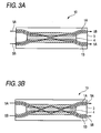
- Figs. 3A and 3B are plan views for indicating switching states of optical paths in the waveguide type liquid crystal optical switch shown in Fig. 1, Fig. 3A shows OFF state, and Fig. 3B shows ON state;
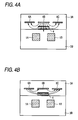
- Figs. 4A and 4B are sectional views for explaining a basic idea of optical path switching operations by the waveguide type liquid crystal optical switch shown in Fig. 1;
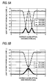
- Figs. 5A and 5B are graphic representation for representing results of measuring changes in light intensity within the cores, Fig. 5A shows that of A-mode coupling, and Fig. 5B shows that of B-mode coupling;
- Fig. 6A is a plan view and Fig. 6B is a sectional view, which are used to explain design examples of the waveguide type liquid crystal optical switches in the A-mode coupling and the B-mode coupling;
- Fig. 7A is an illustration for representing a design example of a waveguide type liquid crystal optical switch employed so as to measure changes in light intensity within a core due to a refractive index difference between upper/lower claddings; and Fig. 7B is a graphic representation for indicating measurement results obtained by measuring both the refractive index difference between the upper/lower claddings, and the changes in the light intensity within the core;
- Fig. 8 is a plan view for showing a double gate type optical switch arranged by connecting four pieces of the waveguide type liquid crystal optical switches to each other; and
- Fig. 9 is a plan view for showing a double gate type optical switch arranged by connecting two pieces of the waveguide type liquid crystal optical switches to each other.
-
- Referring now to drawings, a waveguide type liquid crystal optical switch according to the present invention will be described in detail.
- Fig. 1 is a plan view for indicating a waveguide type liquid crystal
optical switch 10 according to an embodiment of the present invention, as viewed from a core side thereof (namely, lower side of Fig. 2). Fig. 2 is a sectional view of this waveguide type liquid crystaloptical switch 10, taken along a line A-A of Fig. 1. As indicated in the drawings, the waveguide type liquid crystaloptical switch 10 is subdivided into two substrates, namely, anupper substrate 8A and alower substrate 8B. Both afirst core 1A and asecond core 1B are embedded at a predetermined depth position in thislower substrate 8B from a surface of thelower substrate 8B along an axial line direction of thislower substrate 8B. While thefirst core 1A is approached to thesecond core 1B at central portions thereof over predetermined lengths, both thefirst core 1A and thesecond core 1B are located in parallel to each other. Intervals between thefirst core 1A and thesecond core 1B are gradually widened toward edges of both end portions. This approached parallel portion may form a so-called "optical directional coupler." - The
upper substrate 8A and thelower substrate 8B are manufactured by such a material having a refractive index lower than that of a material used to manufacture thefirst core 1A and thesecond core 1B. This material of both theupper substrate 8A and thelower substrate 8B is selected to be, for example, a material of (SiO2 - TiO2) having a refractive index of 1.523. On the other hand, the material of both thefirst core 1A and thesecond core 1B is selected to be, for instance, a material of (SiCl4 - TiCl4) having a refractive index of 1.530. - A concave portion having a rectangular shape as viewed in a sectional plane is formed in a stripe form on a surface of the
upper substrate 8A opposing thelower substrate 8B so that that this concave portion covers a space which is sandwiched by both thefirst core 1A and thesecond core 1B. Anorientation film 7A is formed on a bottom portion of this concave portion, and nematic liquid crystal is filled on thisorientation film 7A. While anotherorientation film 7B is provided on thelower substrate 8B in such a manner that an entire surface of thislower substrate 8B is covered by thisorientation film 7B, the nematic liquid crystal is sealed by joining theupper substrate 8A to thelower substrate 8B by way of a properly-selected opticaladhesive agent 11 to form an integral body, so that athird core 4 is formed. - It should be understood that there is no limitation as to the sort of nematic liquid crystal which constitutes the
third core 4, and therefore, for example, 4- (4-pentylcyclohexyl) cyanobenzene and the like maybe used. Also, the materials of both theorientation film 7A and theorientation film 7B may be selected from any materials known in the technical field. For example, a polyamide film and the like, which have been rubbing-processed, may be used. - Also, a
first electrode 6B is provided in theupper substrate 8A just above thethird core 4 in such a manner that a gap between thefirst core 1A and thesecond core 1B is covered by thisfirst electrode 6B. Furthermore, both asecond electrode 6A and athird electrode 6C are formed on both sides of thefirst electrode 6B. Thefirst electrode 6B, thesecond electrode 6A, and thethird electrode 6C are controllable in an independent manner. Also, both thesecond electrode 6A and thethird electrode 6C may define that the orientation direction of the liquid crystal molecules is intersected perpendicular to the orientation direction of theorientation films - In the waveguide type liquid crystal
optical switch 10 with employment of the above structure, the optical path can be switched (namely, switching operation) between thefirst core 1A and thesecond core 1B by adjusting voltages applied to the first tothird electrodes 6A to 6C so as to control the orientation of the liquid crystal molecules of thethird core 4 . For example, as shown in Fig. 3A, anoptical signal 5A and anotheroptical signal 5B may be penetrated from respective cores provided on the light incident side to thethird core 4, and may be furthermore transferred to other cores. Also, as represented in Fig. 3B, the optical signals which have been transferred to other cores may be again penetrated through thethird core 4, and furthermore, may be transferred to the respective cores provided on the light incident side. In the below-mentioned descriptions, such a case that an entered optical signal is projected from the same core will be referred to as an "ON state (Fig. 3B)", whereas such a case that an entered optical signal is projected from another core will be referred to as an "OFF state (Fig. 3A) ." - While the above-described optical path is switched, as indicated in Fig. 4A, since such potentials having the same phases are applied to both the
second electrode 6A and thethird electrode 6C with respect to thefirst electrode 6B, as indicated by arrows in Fig. 4A, such an electronic field is produced which is directed from thefirst electrode 6B to both thesecond electrode 6A and thethird electrode 6C. As a consequence, in thethird core 4, a vertical electric fieldwith respect to the first electrode 6Bmaybecome dominant. As a result, a change in coupling coefficients with respect to TE polarized light becomes dominant. Also, as indicated in Fig. 4B, since such potentials having the reverse phases are applied to both thesecond electrode 6A and thethird electrode 6C while thefirst electrode 6B is set to the reference potential, as indicated by arrows in Fig. 4B, such a horizontal electric field becomes dominant, which is directed from thesecond electrode 6A to thethird electrode 6C with respect to thethird core 4. As a result, a change in coupling coefficients with respect to TM polarized light becomes dominant. As previously explained, since both the voltages and the phases applied to both thesecond electrode 6A and thethird electrode 6C are adjusted with respect to thefirst electrode 6B, the ON states and the OFF states with respect to both the TE polarized light and the TM polarized light may be adjusted, and thus, there is no polarized-wave depending characteristic. - Generally speaking, since a change contained in refractive indexes of liquid crystal is several ten times larger than a difference contained in the refractive indexes between the material used to form the
cores cladding 3, the above-explained switching operation can be firmly carried out under low voltage. - It should also be noted that the above-described switching modes become reversed in the case that the nematic liquid crystal used in the
third core 4 represents the positive change in the refractive indexes, and represents the negative change in the refractive indexes. - Also, in order to perform the above-explained switching operations in more correct manners, the operation mode of the waveguide type liquid crystal optical switch may be preferably set to either an A-mode coupling or B-mode coupling. Any one of these A-mode and B-mode couplings indicates such a case under the above-described ON state.
- In this A-mode coupling, both the
first core 1A and thesecond core 1B are set as follows: At respective intermediate positions of these first andsecond cores first core 1A) , and light intensity of thethird core 4 may become minimal values, and also, light intensity of the core into which the light is not entered within the first and second cores (for instance,second core 1B) may become a maximum value. In such a coupling mode, a portion of the light entered into thefirst core 1A is transferred via thethird core 4 to thesecond core 1B, and thereafter, is similarly returned via thethird core 4 to thefirst core 1A. - To realize this A-mode coupling, the respective cores must be designed in such a manner that a time period during which the incident light is transferred from the
first core 1A to thesecond core 1B is made coincident with another time period during which the incident light is transferred via thethird core 4 to either thefirst core 1A or thesecond core 1B. One example of this core designing idea is shown as follows: Also, Fig. 5A shows such a measurement result that while a waveguide type liquid crystal optical switch manufactured based upon the below-mentioned design ideas was employed, changes in light intensity of the respective cores were actually measured. It should also be noted that dimensional places are illustrated in Figs. 6A and 6B. W = 8 µm, D = 5 µm, GLC = 1.5 µm, HLC = 1.6 µm, WLC = 8 µm, LLC = 2.97 µm. - In this B-mode coupling, both the
first core 1A and thesecond core 1B are set as follows: At respective intermediate positions of these first andsecond cores first core 1A) may become a minimal value, and also, both light intensity of the core into which the light is not entered within the first and second cores (for instance,second core 1B) and light intensity of thethird core 4 may become maximum values. A designing example capable of realizing the B-mode coupling is shown in the below-mentioned description (dimensional places as illustrated in Figs. 6A and 6B) . This B-mode coupling has such a feature that both thefirst core 1A and thesecond core 1B are formed at such positions within thelower substrate 8B, which are located deeper than those of the A-mode coupling. Also, Fig. 5B shows such a result that while a waveguide type liquid crystal optical switch manufactured based upon the below-mentioned design ideas was employed, changes in light intensity of the respective cores were actually measured. W = 8 µm, D = 5 µm, GLC = 3.9 µm, HLC = 1.6 µm, WLC = 8 µm, LLC = 2.77 µm . - It should also be noted that in the waveguide type liquid crystal
optical switch 10 of the present invention, as previously described, the metal materials such as gold, copper, and aluminum are used as the electrode materials in addition to the transparent electric conductive materials such as SnO2 and ITO. Since light absorptions may occur due to these materials, thefirst core 1A, thesecond core 1B, and the respective electrodes are preferably separated from each other by such a distance longer than, or equal to a half width (W) of each core, desirably substantially equal to this width (W). However, when the distance between the electrodes is increased, the voltage applied so as to orientate the liquid crystal molecules of thethird core 4 must be increased in accordance with this increased distance, so that cost of electric power for switch operations is increased. - In order to solve such a difficulty, it is an effective way to suppress intensity of light distributed at outer sides of the respective electrodes. To this end, the refractive index of the cladding which surrounds both the
first core 1A and thesecond core 1B, and the refractive indexes of the respective electrodes may be made different from each other. In other words, referring again back to Fig. 2, while the cladding 3 (see Fig. 1) may be defined as thelower substrate 8B which surrounds both thefirst core 1A and thesecond core 1B, and theupper substrate 8A which surrounds the first tothird electrodes 6A to 6C and thethird core 4, thelower substrate 8B and theupper substrate 8A are manufactured by employing separate materials having different diffractive indexes. For the sake of easy explanations, theupper substrate 8A will be referred to as an "upper cladding 3A", and thelower substrate 8B will be referred to as a "lower cladding 3B" in the below-mentioned explanations. - In accordance with such a structure, assuming now that the refractive index of the
lower cladding 3B is "NCL1" and the refractive index of theupper cladding 3A is "NCL2", in order that light is not leaked from the cores to the electrode sides (namely, upper/lower directions as viewed in this drawing), such a refractive index condition may be set to (NCL1 - NCL2)>0. The larger (NCL1 - NCL2) is increased, the smaller the light is leaked. The cores and the upper/lower claddings 3A/3B were manufactured by employing the dimensions and the refractive index materials indicated in Fig. 7A, and attenuation amounts of light intensity along a γ-axis direction were measured while ΔNCL = ΔCL1 - NCL2 was employed as a parameter. This measurement result is indicated in Fig. 7B. If there is a refractive index difference (ΔNCL), as compared with such a case that ΔNCL = 0, namely the refractive index of theupper cladding 3A is equal to the refractive index of thelower cladding 3B, then an attenuation of light intensity may appear. The larger the refractive index difference (ΔNCL) is increased, the larger the attenuation of light intensity is increased. In other words, it can be seen that the larger the refractive index difference (ΔNCL) is increased, the lower the light is leaked. - Based upon the above-described experimental result, for example, both the
upper cladding 3A and thelower cladding 3B are formed by employing such a material having a refractive index difference (ΔNCL) of 0.04, whereas therespective electrodes 6A to 6C are formed on theupper cladding 3A while theseelectrodes 6A to 6C are separated by approximately 2 µm from the surface of thelower cladding 3B. Thus, the light intensity on the surfaces of the electrodes is attenuated lower than, or equal to 0.1 % within the cores, so that light absorptions caused these electrodes can be substantially neglected. - Also, in general, since liquid crystal has large temperature dependent characteristics, the optical waveguide type liquid crystal
optical switch 10 may be more preferably provided with a temperature control unit in order to eliminate an adverse influence caused by temperature changes in external environments. As the temperature control unit, a Peltier-effect element is suitable due to easy temperature controlling operation thereof. Although not shown in the drawing, for example, while this Peltier-effect element is provided in the vicinity of thethird core 4 such as, e.g., an upper surface of thelower cladding 3B (otherwise,upper substrate 8A), the entireoptical switch 10 is thermally insulated in addition thereto. Since the temperature variation is suppressed in the above-described manner, such an optical waveguide type liquid crystal optical switch having a low crosstalk and also low insertion loss maybe constituted. - Also, while an even number of the above-explained optical waveguide type liquid crystal
optical switches 10 may be connected to each other, these connected optical switches may be equipped with one pair of input terminals and one pair of output terminals in a similar manner to a single optical switch. In the present invention, such a construction that an even number of waveguide type liquid crystaloptical switches 10 are connected to each other, and the entire optical switches may function as a single optical switch will be defined as a "double gate type optical switch." - Fig. 8 indicates an example of such a double gate type optical switch, and schematically represents the double gate type optical switch which is arranged by four sets of the above-described waveguide type liquid crystal optical switches 10. The double gate type optical switch shown in this drawing is arrangedas follows: That is to say, one output terminal "c" of a first optical waveguide-type liquid crystal
optical switch 10A is connected to one input terminal "e" of a second waveguide type liquid crystaloptical switch 10B by employing anoptical waveguide 20; the other output terminal "d" of the first optical waveguide type liquid crystaloptical switch 10A is connected to one input terminal "m" of a fourth waveguide type liquid crystaloptical switch 10D by employing anoptical waveguide 20; one output terminal "k" of a third optical waveguide type liquid crystaloptical switch 10C is connected to the other input terminal "f" of the second waveguide type liquid crystaloptical switch 10B by employing anoptical waveguide 20; and the other output terminal "1" of the third optical waveguide type liquid crystaloptical switch 10C is connected to the other input terminal "n" of the fourth waveguide type liquid crystaloptical switch 10D by employing anoptical waveguide 20. Also, one input terminal "a" of the first optical waveguide type liquid crystaloptical switch 10A is terminated as a first input port (IN1); one input terminal "j" of the third optical waveguide type liquid crystaloptical switch 10C is terminated as a second input port (IN2); and furthermore, one output terminal "g" of the second optical waveguide type liquid crystaloptical switch 10B is terminated as a first output port (OUT1); and, the other output terminal "p" of the fourth optical waveguide type liquid crystaloptical switch 10D is terminated as a second output port (OUT2). In addition thereto, the other output terminal "h" of the second optical waveguide type liquid crystaloptical switch 10B is terminated as a dummy port "1", and also, the other output terminal "o" of the fourth optical waveguide type liquid crystaloptical switch 10D is terminated as a dummy port "2." - Also, in this double gate type optical switch, similar to the above-described waveguide type liquid crystal optical switch (see Figs. 3A and 3B), such a condition that an optical signal entered from the first input port IN1 is projected from the first output port OUT1, and also, an output signal entered from the second input port IN2 is projected from the second port OUT2 is assumed as an "ON state", whereas conversely, such a condition that an optical signal entered from the first input port IN1 is projected from the second output port OUT2, and also, an output signal entered from the second input port IN2 is projected from the first port OUT1 is assumed as an "OFF state". Also, under either the "ON state" or the "OFF state", a ratio of intensity of an optical signal which should be projected from each of the output ports with respect to intensity of an optical signal (namely, stray light) which should not be projected is defined as an "extinction ratio."
- In the above-described double gate type switch, in order to bring this double gate type switch into the ON state, all of the waveguide type liquid crystal
optical switches 10A to 10D are set to ON states. As a result, the optical signal entered from the first input port IN1 is projected from the output terminal "c" of the first waveguide type liquid crystaloptical switch 10A, and then, is entered to the input terminal "e" of the second optical waveguide switch 103, and thereafter, is projected from the output terminal "g", namely from the first output port OUT1. In this case, even when stray light is present, this stray light is projected from the output terminal "d" in the first waveguide type liquid crystaloptical switch 10A and then is reached to thedummy port 2, and the stray light is reached to thedummy port 1 in the second waveguide type liquid crystaloptical switch 10B, namely, this stray light is not projected from the respective original output ports thereof. As a consequence, a high extinction ratio can be realized. - On the other hand, in order to bring this double gate type optical switch into an OFF state, all of the waveguide type liquid crystal
optical switches 10A to 10D may be merely set to OFF states. In this case, stray light is similarly projected from either thedummy port 1 or thedummy port 2. - Also, as shown in Fig. 9, while two sets of the above-described waveguide type liquid crystal
optical switches 10 are connected to each other, these connected waveguide type liquid crystal optical switches may constitute a single optical switch as an entire construction. In this switch construction, one output terminal "c" of a first optical waveguide type liquid crystaloptical switch 10A is connected to one input terminal "e" of a second waveguide type liquid crystaloptical switch 10B by employing anoptical waveguide 20. Also, in this switch construction, one input terminal "a" of the first optical waveguide type liquid crystaloptical switch 10A is terminated as a first input port (IN1) ; the other input terminal "f" of the second optical waveguide type liquid crystaloptical switch 10B is terminated as a second input port (IN2) ; one output terminal "g" of the second optical waveguide type liquidcrystaloptical switch 10B is terminated as a first output port (OUT1) ; and the other output terminal "d" of the first optical waveguide type liquid crystaloptical switch 10A is terminated as a second output port (OUT2). Further, the other output terminal "h" of the second optical waveguide type liquid crystaloptical switch 10B is terminated as a dummy port. - In the above-described double gate type switch, in order to bring this double gate type switch into the ON state, both the first waveguide type liquid crystal
optical switch 10A and the second waveguide type liquid crystaloptical switch 10B are set to ON states. As a result, an optical signal entered to the first input port IN1 is projected from the output terminal "c" of the first waveguide type liquid crystaloptical switch 10A, and then, is entered to the input terminal "e" of the second optical waveguide type liquid crystaloptical switch 10B, and thereafter, is projected from the output terminal "g", namely from the first output port OUT1. In this case, when stray light is present, this stray light is reached to the other output terminal "d" of the first waveguide type liquid crystaloptical switch 10A and then is projected from the second output port OUT2. As a consequence, an extinction ratio of this double gate type optical switch may become the same as that of a single waveguide type liquid crystal optical switch. - On the other hand, in order to bring this double gate type optical switch into an OFF state, both the first waveguide type liquid crystal
optical switch 10A and the second waveguide type liquid crystaloptical switch 10B are set to OFF states. As a result, any one of stray light as to the optical signals which are entered into the first input port IN1 and the second input port IN2 is outputted from thedummy port 2. - As previously explained, in the double gate type optical switch constituted by two sets of the waveguide type liquid crystal
optical switches - It should also be noted that the above-described double gate type optical switches may be preferably constructed as follows. That is, all of the waveguide type liquid crystal optical switches may be preferably connected to each other by employing the optical waveguides and then are integrated on the same substrate. Alternatively, waveguide type liquid crystal optical switches which have been separately formed may be connected to each other by employing optical fibers so as to construct such double gate type optical switches.
- As previously described in detail, in accordance with the present invention, the high-performance waveguide type liquid crystal optical switches having no polarized-wave dependent characteristic and operable under low insertion loss can be provided, so compared with the conventional optical waveguide type optical switch.
Claims (8)
- A waveguide type liquid crystal optical switch in which optical waveguide formed by cores, comprising:a pair of a first core and a second core, in which light is input from one of the first core and the second core and an optical path is switched between the first and second cores, and the first core and the second core being provided so as to form a space therebetween;a third core provided apart from the first core and the second core at predetermined distances, into which nematic liquid crystal orientated by an orientation film along a predetermined direction is filled, the third core overlapping to the space formed between the first core and the second core;a first electrode arranged on an opposite side of the first core and the second core with respect to the third core in such a manner that the first electrode is overlapped to the space between the first core and the second core;a second electrode and a third electrode, which are arranged on both sides of the first electrode so as to constitute a pair, and which cause liquid crystal molecules to be orientated along a direction perpendicular to the orientation direction of the orientation film; anda cladding for incorporating the first core, the second core, the third core, and the first to third electrodes.
- A waveguide type liquid crystal optical switch as claimed in claim 1, wherein a refractive index of the third core with respect to either TE polarized light or TM polarized light is changeable to thereby switch the optical path between the first core and the second core.
- A waveguide type liquid crystal optical switch as claimed in claim 1, wherein the first and second cores are coupled in a mode coupling where a light intensity of one of the first and second cores to which the light is input and a light intensity of the third core have minimal values and a light intensity of another core to which the light is not input has a maximum value at intermediate positions along respective optical axis directions under a condition that a refractive index of the third core is set to a higher value.
- A waveguide type liquid crystal optical switch as claimed in claim 1, wherein the first and second cores are coupled in a mode coupling where a light intensity of one of the first and second cores to which the light is input has a minimal value and a light intensity of another core to which the light is not input and a light intensity of the third core have maximum values at intermediate positions along respective optical axis directions under a condition that a refractive index of the third core is set to a higher value.
- A waveguide type liquid crystal optical switch as claimed in claim 1, wherein a cladding is defined as a first cladding which surrounds both the first core and the second core, and a second cladding which surrounds the third core and the first to third electrodes; and a refractive index of the first cladding is made higher than a refractive index of the second cladding.
- A waveguide type liquid crystal optical switch as claimed in claim 1, further comprising:a temperature control unit for maintaining a temperature of an optical waveguide at a constant temperature.
- A waveguide type liquid crystal optical switch as claimed in claim 6, wherein the temperature control unit is integrated with the waveguide type liquid crystal optical switch, and is thermally insulated from a surrounding environment thereof.
- A double gate type optical switch comprising two pieces, or four pieces of the waveguide type liquid crystal optical switch recited in Claim 1, wherein an output terminal of one waveguide type liquid crystal optical switch is connected to an input terminal of another waveguide type liquid crystal optical switch by way of either an optical guide path or an optical fiber; and the double gate type optical switch is provided with two input terminals, two output terminals, and either one or two dummy output terminals.
Applications Claiming Priority (2)
| Application Number | Priority Date | Filing Date | Title |
|---|---|---|---|
| JP2002143335 | 2002-05-17 | ||
| JP2002143335A JP2003337317A (en) | 2002-05-17 | 2002-05-17 | Waveguide type liquid crystal optical switch |
Publications (1)
| Publication Number | Publication Date |
|---|---|
| EP1363158A1 true EP1363158A1 (en) | 2003-11-19 |
Family
ID=29267840
Family Applications (1)
| Application Number | Title | Priority Date | Filing Date |
|---|---|---|---|
| EP03011012A Withdrawn EP1363158A1 (en) | 2002-05-17 | 2003-05-16 | Waveguide type liquid crystal optical switch |
Country Status (6)
| Country | Link |
|---|---|
| US (1) | US6763159B2 (en) |
| EP (1) | EP1363158A1 (en) |
| JP (1) | JP2003337317A (en) |
| KR (1) | KR20030089492A (en) |
| CN (1) | CN1458545A (en) |
| CA (1) | CA2429115A1 (en) |
Cited By (1)
| Publication number | Priority date | Publication date | Assignee | Title |
|---|---|---|---|---|
| SG144702A1 (en) * | 2004-01-02 | 2008-08-28 | Sony Corp | An optical switch device and method for forming an optical switch device |
Families Citing this family (32)
| Publication number | Priority date | Publication date | Assignee | Title |
|---|---|---|---|---|
| US20030179998A1 (en) * | 2002-03-22 | 2003-09-25 | Jianjun Zhang | Switchable bragg grating filter |
| US6891989B2 (en) * | 2001-10-22 | 2005-05-10 | Integrated Optics Communications Corporation | Optical switch systems using waveguide grating-based wavelength selective switch modules |
| US6973231B2 (en) * | 2001-10-22 | 2005-12-06 | International Optics Communications Corporation | Waveguide grating-based wavelength selective switch actuated by thermal mechanism |
| US20030123798A1 (en) * | 2001-12-10 | 2003-07-03 | Jianjun Zhang | Wavelength-selective optical switch with integrated Bragg gratings |
| JP2003241240A (en) * | 2002-02-14 | 2003-08-27 | Nippon Sheet Glass Co Ltd | Waveguide type liquid crystal optical switch |
| US20040228574A1 (en) * | 2003-05-14 | 2004-11-18 | Yu Chen | Switchable optical dispersion compensator using Bragg-grating |
| CN1794922A (en) * | 2003-06-26 | 2006-06-28 | 三菱化学株式会社 | Polyglycerol fatty acid ester and emulsified or solubilized composition containing it |
| US20050018964A1 (en) * | 2003-07-24 | 2005-01-27 | Yu Chen | Compensation of Bragg wavelength shift in a grating assisted direct coupler |
| US20050271325A1 (en) * | 2004-01-22 | 2005-12-08 | Anderson Michael H | Liquid crystal waveguide having refractive shapes for dynamically controlling light |
| US8860897B1 (en) | 2004-01-22 | 2014-10-14 | Vescent Photonics, Inc. | Liquid crystal waveguide having electric field orientated for controlling light |
| US8989523B2 (en) | 2004-01-22 | 2015-03-24 | Vescent Photonics, Inc. | Liquid crystal waveguide for dynamically controlling polarized light |
| US8463080B1 (en) | 2004-01-22 | 2013-06-11 | Vescent Photonics, Inc. | Liquid crystal waveguide having two or more control voltages for controlling polarized light |
| JP2005266482A (en) * | 2004-03-19 | 2005-09-29 | Fujitsu Ltd | Optical switching element, manufacturing method thereof, and control method of optical switching element |
| US20050265720A1 (en) * | 2004-05-28 | 2005-12-01 | Peiching Ling | Wavelength division multiplexing add/drop system employing optical switches and interleavers |
| US7525663B2 (en) * | 2004-08-20 | 2009-04-28 | Resmed Limited | Method and apparatus for humidification of breathable gas by condensation and/or dehumidification |
| KR100831565B1 (en) * | 2004-09-10 | 2008-05-21 | 주식회사 케이티 | Liquid crystal injection device for hollow fiber and liquid crystal injection method of hollow fiber |
| US7570320B1 (en) * | 2005-09-01 | 2009-08-04 | Vescent Photonics, Inc. | Thermo-optic liquid crystal waveguides |
| US9366938B1 (en) * | 2009-02-17 | 2016-06-14 | Vescent Photonics, Inc. | Electro-optic beam deflector device |
| WO2011053626A2 (en) * | 2009-10-30 | 2011-05-05 | Cornell University | Optofluidic apparatus, method, and application |
| JP5691033B2 (en) * | 2009-12-25 | 2015-04-01 | 学校法人慶應義塾 | Waveguide type optical gate switch |
| US8995038B1 (en) | 2010-07-06 | 2015-03-31 | Vescent Photonics, Inc. | Optical time delay control device |
| JP6031785B2 (en) * | 2012-03-19 | 2016-11-24 | 富士通株式会社 | Optical switch device and control method thereof |
| US20160306256A1 (en) * | 2015-04-15 | 2016-10-20 | Chen-Kuo Sun | Method for configuring an optical modulator |
| US9500929B2 (en) * | 2015-04-15 | 2016-11-22 | Chen-Kuo Sun | Vertical electro-optically coupled switch |
| US10036855B1 (en) * | 2017-07-13 | 2018-07-31 | Chen-Kuo Sun | Reverse bias modulating waveguide/diode |
| US10126496B1 (en) | 2017-07-13 | 2018-11-13 | Chen-Kuo Sun | Reverse bias modulating multi-material waveguide/diode |
| US10409137B2 (en) | 2017-08-22 | 2019-09-10 | Chen-Kuo Sun | System and method for controlling energy flux modulation |
| US10976579B2 (en) * | 2018-08-09 | 2021-04-13 | Analog Devices, Inc. | Liquid crystal waveguide with active incoupling |
| JP7123769B2 (en) * | 2018-11-28 | 2022-08-23 | 京セラ株式会社 | light switch |
| US10816832B1 (en) | 2019-09-04 | 2020-10-27 | Veo, Inc. | Optical phase shifter using fine lithography defined volumetric junctions |
| CN114563884B (en) * | 2022-02-25 | 2024-05-14 | 南方科技大学 | Segmented driving method for quick response of nematic liquid crystal molecules |
| DE102023206495B3 (en) * | 2023-07-07 | 2024-11-21 | Volkswagen Aktiengesellschaft | Integrated circuit, arrangement and method for coupling optical signals into an integrated circuit |
Citations (5)
| Publication number | Priority date | Publication date | Assignee | Title |
|---|---|---|---|---|
| US4749258A (en) * | 1985-11-05 | 1988-06-07 | Alcatel Usa Corporation | Liquid crystal optical cross point switching device |
| EP0317531A1 (en) * | 1987-11-20 | 1989-05-24 | Telefonaktiebolaget L M Ericsson | Method of disposing a polarization directing optoelectronic coupler and a coupler for carrying out the method |
| US5044712A (en) * | 1990-06-29 | 1991-09-03 | The United States Of America As Represented By The Secretary Of The Air Force | Waveguided electrooptic switches using ferroelectric liquid crystals |
| JPH05165068A (en) * | 1991-12-18 | 1993-06-29 | Nikko Kyodo Co Ltd | Optical switch |
| EP1054288A2 (en) * | 1999-05-21 | 2000-11-22 | Agilent Technologies Inc. | Programmable light path device |
Family Cites Families (4)
| Publication number | Priority date | Publication date | Assignee | Title |
|---|---|---|---|---|
| US5596671A (en) * | 1994-04-28 | 1997-01-21 | Rockwell, Iii; Marshall A. | Optical waveguide display system |
| US5586205A (en) * | 1995-04-10 | 1996-12-17 | National Science Council | Apparatus for selecting waveguide modes in optical fiber and the method of manufacturing the same |
| US6546163B2 (en) * | 2000-10-09 | 2003-04-08 | John I. Thackara | Planar waveguide switch and optical cross-connect |
| JP2003241240A (en) * | 2002-02-14 | 2003-08-27 | Nippon Sheet Glass Co Ltd | Waveguide type liquid crystal optical switch |
-
2002
- 2002-05-17 JP JP2002143335A patent/JP2003337317A/en active Pending
-
2003
- 2003-05-16 KR KR10-2003-0031080A patent/KR20030089492A/en not_active Withdrawn
- 2003-05-16 EP EP03011012A patent/EP1363158A1/en not_active Withdrawn
- 2003-05-16 US US10/438,877 patent/US6763159B2/en not_active Expired - Fee Related
- 2003-05-16 CA CA002429115A patent/CA2429115A1/en not_active Abandoned
- 2003-05-19 CN CN03136241A patent/CN1458545A/en active Pending
Patent Citations (5)
| Publication number | Priority date | Publication date | Assignee | Title |
|---|---|---|---|---|
| US4749258A (en) * | 1985-11-05 | 1988-06-07 | Alcatel Usa Corporation | Liquid crystal optical cross point switching device |
| EP0317531A1 (en) * | 1987-11-20 | 1989-05-24 | Telefonaktiebolaget L M Ericsson | Method of disposing a polarization directing optoelectronic coupler and a coupler for carrying out the method |
| US5044712A (en) * | 1990-06-29 | 1991-09-03 | The United States Of America As Represented By The Secretary Of The Air Force | Waveguided electrooptic switches using ferroelectric liquid crystals |
| JPH05165068A (en) * | 1991-12-18 | 1993-06-29 | Nikko Kyodo Co Ltd | Optical switch |
| EP1054288A2 (en) * | 1999-05-21 | 2000-11-22 | Agilent Technologies Inc. | Programmable light path device |
Non-Patent Citations (1)
| Title |
|---|
| PATENT ABSTRACTS OF JAPAN vol. 017, no. 566 (P - 1629) 14 October 1993 (1993-10-14) * |
Cited By (1)
| Publication number | Priority date | Publication date | Assignee | Title |
|---|---|---|---|---|
| SG144702A1 (en) * | 2004-01-02 | 2008-08-28 | Sony Corp | An optical switch device and method for forming an optical switch device |
Also Published As
| Publication number | Publication date |
|---|---|
| JP2003337317A (en) | 2003-11-28 |
| CA2429115A1 (en) | 2003-11-17 |
| US6763159B2 (en) | 2004-07-13 |
| KR20030089492A (en) | 2003-11-21 |
| CN1458545A (en) | 2003-11-26 |
| US20030219197A1 (en) | 2003-11-27 |
Similar Documents
| Publication | Publication Date | Title |
|---|---|---|
| US6763159B2 (en) | Waveguide type liquid crystal optical switch | |
| US6687425B2 (en) | Waveguides and devices incorporating optically functional cladding regions | |
| JP4711351B2 (en) | Light modulator | |
| US5263102A (en) | Polarization-independent optical switches/modulators | |
| US5185830A (en) | Optical waveguide directional coupler including control electrodes | |
| EP0669546B1 (en) | Waveguide-type optical device | |
| JP5467414B2 (en) | Optical functional waveguide | |
| WO2003010592A3 (en) | Waveguides and devices incorporating optically functional cladding regions | |
| US4172630A (en) | Multimode electrooptic waveguide switch | |
| US6904207B2 (en) | Waveguide type liquid-crystal optical switch | |
| US6842573B2 (en) | Directional optical coupler | |
| JP2003222915A (en) | Waveguide type liquid crystal optical switch | |
| JP2003222916A (en) | Waveguide type liquid crystal optical switch | |
| JPH01201628A (en) | Optical switch | |
| EP0494751B1 (en) | Directional coupler type optical function element | |
| JP2659786B2 (en) | Mode light separator | |
| JPS6294823A (en) | Waveguide type optical modulator | |
| RU2451959C2 (en) | Low switching voltage, fast time response digital optical switch | |
| JPS62145224A (en) | Optical waveguide device | |
| JPH05224246A (en) | Optical control device | |
| JP2004053872A (en) | Waveguide type liquid crystal variable optical attenuator | |
| JPH04234733A (en) | Directional coupler type optical function element | |
| JP2004126244A (en) | Optical waveguide having switching function and connecting structure of optical fiber | |
| JPH0367229A (en) | light switch |
Legal Events
| Date | Code | Title | Description |
|---|---|---|---|
| PUAI | Public reference made under article 153(3) epc to a published international application that has entered the european phase |
Free format text: ORIGINAL CODE: 0009012 |
|
| AK | Designated contracting states |
Kind code of ref document: A1 Designated state(s): AT BE BG CH CY CZ DE DK EE ES FI FR GB GR HU IE IT LI LU MC NL PT RO SE SI SK TR |
|
| AX | Request for extension of the european patent |
Extension state: AL LT LV MK |
|
| AKX | Designation fees paid | ||
| REG | Reference to a national code |
Ref country code: DE Ref legal event code: 8566 |
|
| STAA | Information on the status of an ep patent application or granted ep patent |
Free format text: STATUS: THE APPLICATION IS DEEMED TO BE WITHDRAWN |
|
| 18D | Application deemed to be withdrawn |
Effective date: 20040520 |