EP1362353B1 - Layered structure, sensor and method of producing and use of the same - Google Patents
Layered structure, sensor and method of producing and use of the same Download PDFInfo
- Publication number
- EP1362353B1 EP1362353B1 EP02710074A EP02710074A EP1362353B1 EP 1362353 B1 EP1362353 B1 EP 1362353B1 EP 02710074 A EP02710074 A EP 02710074A EP 02710074 A EP02710074 A EP 02710074A EP 1362353 B1 EP1362353 B1 EP 1362353B1
- Authority
- EP
- European Patent Office
- Prior art keywords
- layered structure
- conductive polymer
- substrate material
- change
- layer
- Prior art date
- Legal status (The legal status is an assumption and is not a legal conclusion. Google has not performed a legal analysis and makes no representation as to the accuracy of the status listed.)
- Expired - Lifetime
Links
- 229920001940 conductive polymer Polymers 0.000 claims abstract description 63
- 239000000758 substrate Substances 0.000 claims abstract description 41
- 239000000463 material Substances 0.000 claims abstract description 39
- 238000007639 printing Methods 0.000 claims abstract description 30
- 230000008859 change Effects 0.000 claims abstract description 28
- 238000006243 chemical reaction Methods 0.000 claims abstract description 24
- 238000000034 method Methods 0.000 claims abstract description 18
- 239000002861 polymer material Substances 0.000 claims abstract description 14
- 238000004519 manufacturing process Methods 0.000 claims abstract description 12
- 238000004528 spin coating Methods 0.000 claims abstract description 4
- 229920000767 polyaniline Polymers 0.000 claims description 13
- 238000007650 screen-printing Methods 0.000 claims description 3
- 238000005266 casting Methods 0.000 abstract description 2
- 238000005507 spraying Methods 0.000 abstract description 2
- 238000000608 laser ablation Methods 0.000 abstract 1
- 239000010410 layer Substances 0.000 description 28
- 239000007788 liquid Substances 0.000 description 8
- 239000011247 coating layer Substances 0.000 description 6
- 238000005520 cutting process Methods 0.000 description 4
- 239000000203 mixture Substances 0.000 description 4
- 229920000642 polymer Polymers 0.000 description 4
- YXFVVABEGXRONW-UHFFFAOYSA-N Toluene Chemical compound CC1=CC=CC=C1 YXFVVABEGXRONW-UHFFFAOYSA-N 0.000 description 3
- 238000000576 coating method Methods 0.000 description 3
- 238000001723 curing Methods 0.000 description 3
- 229920006267 polyester film Polymers 0.000 description 3
- 239000000126 substance Substances 0.000 description 3
- PAYRUJLWNCNPSJ-UHFFFAOYSA-N Aniline Chemical compound NC1=CC=CC=C1 PAYRUJLWNCNPSJ-UHFFFAOYSA-N 0.000 description 2
- 229920001609 Poly(3,4-ethylenedioxythiophene) Polymers 0.000 description 2
- 239000011248 coating agent Substances 0.000 description 2
- 239000002131 composite material Substances 0.000 description 2
- 229920000775 emeraldine polymer Polymers 0.000 description 2
- 239000011810 insulating material Substances 0.000 description 2
- 239000004065 semiconductor Substances 0.000 description 2
- QAOWNCQODCNURD-UHFFFAOYSA-N Sulfuric acid Chemical compound OS(O)(=O)=O QAOWNCQODCNURD-UHFFFAOYSA-N 0.000 description 1
- 238000003848 UV Light-Curing Methods 0.000 description 1
- 239000000370 acceptor Substances 0.000 description 1
- 239000002253 acid Substances 0.000 description 1
- 150000007513 acids Chemical class 0.000 description 1
- 230000004913 activation Effects 0.000 description 1
- HSFWRNGVRCDJHI-UHFFFAOYSA-N alpha-acetylene Natural products C#C HSFWRNGVRCDJHI-UHFFFAOYSA-N 0.000 description 1
- 150000001491 aromatic compounds Chemical class 0.000 description 1
- 239000003990 capacitor Substances 0.000 description 1
- 230000003197 catalytic effect Effects 0.000 description 1
- 238000004891 communication Methods 0.000 description 1
- 239000002322 conducting polymer Substances 0.000 description 1
- 239000004020 conductor Substances 0.000 description 1
- 238000010276 construction Methods 0.000 description 1
- 238000011109 contamination Methods 0.000 description 1
- 238000007796 conventional method Methods 0.000 description 1
- 238000005536 corrosion prevention Methods 0.000 description 1
- 230000007423 decrease Effects 0.000 description 1
- 238000000151 deposition Methods 0.000 description 1
- 230000008021 deposition Effects 0.000 description 1
- 239000006185 dispersion Substances 0.000 description 1
- 239000012799 electrically-conductive coating Substances 0.000 description 1
- 238000005530 etching Methods 0.000 description 1
- 239000007789 gas Substances 0.000 description 1
- 238000007646 gravure printing Methods 0.000 description 1
- 239000001257 hydrogen Substances 0.000 description 1
- 229910052739 hydrogen Inorganic materials 0.000 description 1
- 238000003384 imaging method Methods 0.000 description 1
- 239000012212 insulator Substances 0.000 description 1
- 230000003993 interaction Effects 0.000 description 1
- 238000005259 measurement Methods 0.000 description 1
- 239000002184 metal Substances 0.000 description 1
- 238000005065 mining Methods 0.000 description 1
- 238000002156 mixing Methods 0.000 description 1
- 238000012544 monitoring process Methods 0.000 description 1
- 238000007645 offset printing Methods 0.000 description 1
- 230000003287 optical effect Effects 0.000 description 1
- 230000003647 oxidation Effects 0.000 description 1
- 238000007254 oxidation reaction Methods 0.000 description 1
- 230000001590 oxidative effect Effects 0.000 description 1
- 229920003023 plastic Polymers 0.000 description 1
- 229920001197 polyacetylene Polymers 0.000 description 1
- 238000006116 polymerization reaction Methods 0.000 description 1
- 230000008569 process Effects 0.000 description 1
- 230000005855 radiation Effects 0.000 description 1
- 238000011946 reduction process Methods 0.000 description 1
- 238000003860 storage Methods 0.000 description 1
- 229920005613 synthetic organic polymer Polymers 0.000 description 1
- 238000012360 testing method Methods 0.000 description 1
- 238000001029 thermal curing Methods 0.000 description 1
- 230000036962 time dependent Effects 0.000 description 1
Images
Classifications
-
- B—PERFORMING OPERATIONS; TRANSPORTING
- B32—LAYERED PRODUCTS
- B32B—LAYERED PRODUCTS, i.e. PRODUCTS BUILT-UP OF STRATA OF FLAT OR NON-FLAT, e.g. CELLULAR OR HONEYCOMB, FORM
- B32B29/00—Layered products comprising a layer of paper or cardboard
-
- Y—GENERAL TAGGING OF NEW TECHNOLOGICAL DEVELOPMENTS; GENERAL TAGGING OF CROSS-SECTIONAL TECHNOLOGIES SPANNING OVER SEVERAL SECTIONS OF THE IPC; TECHNICAL SUBJECTS COVERED BY FORMER USPC CROSS-REFERENCE ART COLLECTIONS [XRACs] AND DIGESTS
- Y10—TECHNICAL SUBJECTS COVERED BY FORMER USPC
- Y10S—TECHNICAL SUBJECTS COVERED BY FORMER USPC CROSS-REFERENCE ART COLLECTIONS [XRACs] AND DIGESTS
- Y10S428/00—Stock material or miscellaneous articles
- Y10S428/901—Printed circuit
-
- Y—GENERAL TAGGING OF NEW TECHNOLOGICAL DEVELOPMENTS; GENERAL TAGGING OF CROSS-SECTIONAL TECHNOLOGIES SPANNING OVER SEVERAL SECTIONS OF THE IPC; TECHNICAL SUBJECTS COVERED BY FORMER USPC CROSS-REFERENCE ART COLLECTIONS [XRACs] AND DIGESTS
- Y10—TECHNICAL SUBJECTS COVERED BY FORMER USPC
- Y10S—TECHNICAL SUBJECTS COVERED BY FORMER USPC CROSS-REFERENCE ART COLLECTIONS [XRACs] AND DIGESTS
- Y10S428/00—Stock material or miscellaneous articles
- Y10S428/913—Material designed to be responsive to temperature, light, moisture
-
- Y—GENERAL TAGGING OF NEW TECHNOLOGICAL DEVELOPMENTS; GENERAL TAGGING OF CROSS-SECTIONAL TECHNOLOGIES SPANNING OVER SEVERAL SECTIONS OF THE IPC; TECHNICAL SUBJECTS COVERED BY FORMER USPC CROSS-REFERENCE ART COLLECTIONS [XRACs] AND DIGESTS
- Y10—TECHNICAL SUBJECTS COVERED BY FORMER USPC
- Y10T—TECHNICAL SUBJECTS COVERED BY FORMER US CLASSIFICATION
- Y10T428/00—Stock material or miscellaneous articles
- Y10T428/24—Structurally defined web or sheet [e.g., overall dimension, etc.]
- Y10T428/24479—Structurally defined web or sheet [e.g., overall dimension, etc.] including variation in thickness
- Y10T428/24612—Composite web or sheet
-
- Y—GENERAL TAGGING OF NEW TECHNOLOGICAL DEVELOPMENTS; GENERAL TAGGING OF CROSS-SECTIONAL TECHNOLOGIES SPANNING OVER SEVERAL SECTIONS OF THE IPC; TECHNICAL SUBJECTS COVERED BY FORMER USPC CROSS-REFERENCE ART COLLECTIONS [XRACs] AND DIGESTS
- Y10—TECHNICAL SUBJECTS COVERED BY FORMER USPC
- Y10T—TECHNICAL SUBJECTS COVERED BY FORMER US CLASSIFICATION
- Y10T428/00—Stock material or miscellaneous articles
- Y10T428/31504—Composite [nonstructural laminate]
- Y10T428/31971—Of carbohydrate
- Y10T428/31993—Of paper
Definitions
- the present invention relates to a layered structure comprising at least two material layers, a sensor, a method for producing layered structure and its use.
- Conductive polymers are materials which have been made conductive by doping with suitable substance. In the doping process both electron acceptors and donors react with polymer structure resulting in highly conducting derivatives. These reactions are called 'doping' in analogy to semiconductors, though they are closer to solid-state chemical reactions.
- Another method for generating electrical conductivity in polymers is blending in which conductive polymer and insulating material are mixed. Electrical properties of conductive polymers can be changed over the full range of conductivity from insulators to metallic conductors.
- An example of a conductive polymer is polyaniline which is a synthetic organic polymer obtained by the chemical or electrochemical oxidative polymerization of aniline.
- Emeraldine base which is the most stable insulating form of polyaniline, can be made conducting either by oxidation or by expose of functional protonic acids e.g. HCl or H 2 SO 4 .
- the conducting emeraldine can be made less conducting or even insulating by a dedoping reaction caused by a reduction process or by exposure to alkaline materials.
- conductive polymers there are wide prospects of using conductive polymers in variety of consumer products. Examples of known use of conductive polymers are batteries, electrical circuits, capacitors, EMI shields, organic LEDs, corrosion prevention products and antistatic products for use in e.g. package industry, construction, clothes, automotive industry, mining.
- US Patent 5,783,111 discloses compositions comprising electrically conducting polyaniline and particular substituted aromatic compounds that simultaneously form hydrogen bonds and ring-ring interactions with, respectively, the NH-groups and the six-membered rings of the conducting polyanilines.
- the conducting polyaniline compositions show drastically enhanced processibility and their blends with insulating or semiconducting materials exhibit significantly improved electrical properties.
- US Patent 5,656,081 discloses a press for printing an electrical circuit component directly on a substrate with an electrically conductive liquid.
- a method of making such a press includes the steps of providing a press surface and engraving the press surface with the plurality of liquid carrying cells which are in liquid communication with each other in both the printing direction and in the transverse direction.
- US Patent 5,622,652 discloses electrically conductive liquid for directly printing an electrical circuit component onto a substrate and a method for making such a liquid.
- the invention relates to an electrically conductive liquid which, when printed onto a substrate is capable of carrying out an electrical circuit function. Using the method there is no need for post-printing steps such as metal etching, catalytic ink activation or electroless deposition.
- US-A-4, 638,286 describes a reactive gas sensor which utilizes an electrically conductive polymer composite including e.g. doped polyacetylene.
- US-A-5,421,959 describes a composite comprising a paper and a conjugated electroconducting polymer.
- EP 0758 671 A2 describes electrically conductive elements, such as imaging elements, which can be prepared by applying electrically conductive coating compositions to a suitable support.
- the object of the present invention is to provide a novel layered structure comprising active substrate and conductive polymer material.
- Another object of the present invention is to provide a method for producing the layered structure comprising active substrate and conductive polymer material.
- a further object of the present invention is to provide a sensor comprising layered structure according to the invention.
- the layered structure according to the invention is mainly characterized in that the layered structure is formed of a doped conductive polymer on a paper substrate material layer to cause a dedoping reaction in the conductive polymer material when the layered structure is exposed to open air or humidity.
- the method for producing layered structure is characterized by applying the conductive polymer material on the substrate material by printing or spin coating or a combination of these.
- the sensor according to the invention comprising an electric device short circuited by the conductive polymer of the layered structure is characterized in that a change in the conductive polymer initiates a change in the function of the electric device.
- the layered structure according to the invention comprising at least two material layers, is formed of a conducting polymer on a substrate material layer and said substrate material has the property of catalysing changes in the conductive polymer when the layered structure experiences a change in its surrounding environment. Further, said substrate material causes a dedoping reaction in the conductive polymer.
- the substrate material allows a reaction in a conductive polymer, such as polyaniline, and the conductivity and/or optical property and/or color of the conductive polymer changes when the layered structure becomes exposed to the surrounding conditions, e.g. to open air or humidity.
- the parameters affecting the reaction are e.g. substrate material properties, such as acidity, porosity and thickness, as well as surrounding conditions, such as humidity, UV radiation and temperature, and also properties of the layered structure such as coating.
- substrate material properties such as acidity, porosity and thickness
- surrounding conditions such as humidity, UV radiation and temperature
- Coating and coating methods also affect the reaction. This phenomenon found in the layered structure according to the invention can be utilized in various ways.
- the substrate material is paper or material with at least one component of paper or other substrate material with suitable properties.
- Geometrical properties of the polymer layer in the layered structure also affect the rate of the reaction and thus the time dependent behaviour of the conductivity of the conductive polymer.
- By adjusting the horizontal and vertical dimensions of the conductive polymer layer it is possible to choose the time scale during which the desired reaction occurs. This phenomenon has been demonstrated in Fig. 5 .
- Manufacturing methods for the layered structure in which conductive polymer material is added on substrate surface according to the invention are e.g. the conventional methods for manufacturing of electrical circuits, i.e., spin coating or printing methods such as gravure, flexographic, offset, digital, or silk screen printing method or a combination of these.
- Utilizing the present invention makes it possible to produce inexpensive indicator components printed on substrate material. These components can be widely used for example in consumer products.
- the elasticity of the layered structure gives it flexural strength which allows its use in applications in which the layered structure may be bent.
- One of the main advantages of the present invention is that the phenomenon occurring in the layered structure is detectable visually as well as instrumentally.
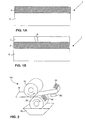
- FIG. 1A shows an example of a layered structure according to the invention.
- the layered structure L comprises a substrate layer S and a conductive polymer layer P.
- the substrate layer S is paper.
- an intermediate layer is generated between the substrate layer S and conductive polymer layer P.
- This intermediate layer adjusts the reaction rate in the conductive polymer layer P by enabling or disabling the passage of the environment factors to the layered structure L.
- the intermediate layer may also be an integral part of the substrate layer S.
- Figure 1B shows a layered structure with a coating layer T.
- a breakage B through which the layered structure is exposed to the surrounding conditions.
- the resistance of the conductive polymer layer P starts increasing. This change in resistance can be measured using conventional measurement devices, and also the change in colour of the conductive polymer can be detected visually.
- Fig. 1B shows the coating layer T on top of the conductive polymer layer P, it is to be understood that the coating layer T can alternatively be on top of the substrate layer S or on both sides of the layered structure L.
- Fig. 2 shows an example of a printing system in which the layered structure according to the invention is produced.
- the web W of substrate material enters the printing unit 100 which comprises an impression cylinder 10, a printing cylinder 20 and a container 40.
- the surface of the printing cylinder 20 is provided with printing elements 50.
- the ink container 40 contains conductive polymer material liquid which is passed via the printing elements 50 on the web W to form layered structures 30 according to the invention.
- the printing system comprising a printing cylinder may be a gravure printing system, flexographic printing system, an offset printing system, or an electrographic printing system.
- other printing methods can be applied according to the invention, e.g. digital or silk screen printing method or stamping as well as spraying and casting methods.
- the printing system 100 may also contain a curing unit 60 which cures the web W by e.g. thermal curing or UV curing or other known curing method.
- the curing unit 60 may be placed on either side of the web or on both sides.
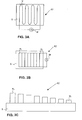
- Figure 3A shows another application of the layered structure according to the invention.
- A1 wire w forms a continuous pattern packed in small area.
- the change in resistance of the wire w catalysed by the substrate S is measured using the measuring equipment M and information of the change of resistance is achieved.
- Figure 3B shows an application of the layered structure according to the invention.
- A2 wires w 1 ,...,w n composed of the conductive polymer are printed on the substrate layer S and they are electrically connected in parallel.
- the total resistance of the parallel connection of the wires w 1 ,...,w n is measured using the measuring equipment M which is e.g. a typical resistance meter.
- the measuring equipment M which is e.g. a typical resistance meter.
- Figure 3C shows a magnified cross-cutting of the layered structure application A2.
- Fig. 3C shows the vertical variance in thickness of wires w 1 ,...,w n .
- the first wire W 1 possesses the greatest vertical thickness and therefore the reaction causing the change of conductivity in the layered structure according to the invention occurs slowest.
- the reaction is faster and depends in each wire on the vertical amount of the conductive polymer in the wires. Therefore the total resistance increases gradually in a non-linear or step-wise manner and the total time elapsed from the exposure of the layered structure application to the surrounding conditions can be estimated in fairly good accuracy.
- the change in resistance of the wires w 1 ,...,w n is also detectable visually by the change of the colour of the wires.
- the reaction rate can be adjusted in a desired way. This way the time scale in which the reaction occurs can be chosen depending the purpose or use of the layered structure application A2.
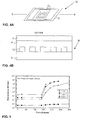
- Fig. 4A shows an example of a sensor according to the invention and Fig. 4B shows a cross cutting of the sensor.
- the sensor 30 comprises an electric device which in this example is a conventional RF tag C A printed or manufactured on the substrate material S using any known method. This type of an RF tag may act as an alarm means in a package.
- the RF tag C A comprises a conductive polymer layer P which, with the substrate layer S, forms a layered structure according to the invention.
- the conductive polymer layer P is covered with the coating layer T. As long as the conductive polymer layer P is intact, it is in conductive state and the RF tag C A is short circuited.
- the layered structure becomes exposed to the surrounding conditions through a breakage conductive polymer P loses its conductivity due to the reaction characteristic for the layered structure according to the invention.
- This causes the RF tag C A turning into an RF circuit which is readable with any known RF tag indicating method.
- the signal given by the RF circuit indicates the breakage of the package.
- the condition of the package can be monitored in any state of e.g. the transport chain or storage.
- the monitoring gives information of the breakage of the package or unauthorised opening of the package depending the positioning of the sensor on the package surface.
- a gravure cylinder was manufactured for the trial runs.
- the gravure cylinder contained line and pattern structures of various dimensions.
- the cell depths of the gravure cylinder were 22 ⁇ m, 33 ⁇ m, 45 ⁇ m, 80/85 ⁇ m and 140/160 ⁇ m.
- the achieved line widths of the conductive polymer varied from 60 ⁇ m to 1 mm and the thickness of the conductive polymer varied from 0.1 to 10 ⁇ m.
- the machine speed of the pilot printing machine in the trial runs was up to 100 m/min.
- the gravure cylinder was used in the printing machine and three different conductive polymer materials were used in printing on polyester film with external chemical treatment and on a paper.
- the ink materials were polytiophene in a form of PEDT/PSS dispersion, SOL-GEL PEDOT liquid and polyaniline based PANI/DBSA toluene.
- paper and polyester film proved to be a suitable substrate material for conductive polymer components. All tested conductive polymer materials were found to be suitable for printing in the test printing machine.
- the behaviour of the printed structures was followed for some time in the printed material. It was found out that the conductivity of the printed polyaniline patterns was changed in time and at the same time the colour of the printed patterns was changing. When the substrate material was paper the color and the conductivity were changing. When the substrate material was a polyester film only a minor change was detected during the followed period.
- Figure 5 shows the measured change in resistance in the layered structure according to the invention.
- Four samples of polyaniline printed on paper were followed for 250 hours. The thickness of the samples varied so that the sample 1 in Fig. 5 was thinnest and the sample 4 was thickest. The samples were kept in the plastic bag for the first 139 hours and then they were left in open air. In the sample 4 with the thickest layer of polyaniline the reaction occurred slowest and no big change is seen. In the samples 1, 2, 3 with thinner layer of polyaniline the reaction was faster depending on the layer thickness. Curves in Fig. 5 show clearly the change in resistance when the samples are moved to open air.
Landscapes
- Laminated Bodies (AREA)
- Investigating Or Analyzing Materials By The Use Of Fluid Adsorption Or Reactions (AREA)
- Inks, Pencil-Leads, Or Crayons (AREA)
- Solid State Image Pick-Up Elements (AREA)
- Glass Compositions (AREA)
- Arrangements For Transmission Of Measured Signals (AREA)
- Non-Insulated Conductors (AREA)
Abstract
Description
- The present invention relates to a layered structure comprising at least two material layers, a sensor, a method for producing layered structure and its use.
- Conductive polymers are materials which have been made conductive by doping with suitable substance. In the doping process both electron acceptors and donors react with polymer structure resulting in highly conducting derivatives. These reactions are called 'doping' in analogy to semiconductors, though they are closer to solid-state chemical reactions. Another method for generating electrical conductivity in polymers is blending in which conductive polymer and insulating material are mixed. Electrical properties of conductive polymers can be changed over the full range of conductivity from insulators to metallic conductors. An example of a conductive polymer is polyaniline which is a synthetic organic polymer obtained by the chemical or electrochemical oxidative polymerization of aniline. Emeraldine base, which is the most stable insulating form of polyaniline, can be made conducting either by oxidation or by expose of functional protonic acids e.g. HCl or H2SO4. Correspondingly, the conducting emeraldine can be made less conducting or even insulating by a dedoping reaction caused by a reduction process or by exposure to alkaline materials. There are wide prospects of using conductive polymers in variety of consumer products. Examples of known use of conductive polymers are batteries, electrical circuits, capacitors, EMI shields, organic LEDs, corrosion prevention products and antistatic products for use in e.g. package industry, construction, clothes, automotive industry, mining.
- Conductive polymers, materials and products are known in the art from many patent publications of which some of them are disclosed in the following.
-
US Patent 5,783,111 discloses compositions comprising electrically conducting polyaniline and particular substituted aromatic compounds that simultaneously form hydrogen bonds and ring-ring interactions with, respectively, the NH-groups and the six-membered rings of the conducting polyanilines. The conducting polyaniline compositions show drastically enhanced processibility and their blends with insulating or semiconducting materials exhibit significantly improved electrical properties. -
US Patent 5,656,081 discloses a press for printing an electrical circuit component directly on a substrate with an electrically conductive liquid. A method of making such a press includes the steps of providing a press surface and engraving the press surface with the plurality of liquid carrying cells which are in liquid communication with each other in both the printing direction and in the transverse direction. -
US Patent 5,622,652 discloses electrically conductive liquid for directly printing an electrical circuit component onto a substrate and a method for making such a liquid. The invention relates to an electrically conductive liquid which, when printed onto a substrate is capable of carrying out an electrical circuit function. Using the method there is no need for post-printing steps such as metal etching, catalytic ink activation or electroless deposition.US-A-4, 638,286 describes a reactive gas sensor which utilizes an electrically conductive polymer composite including e.g. doped polyacetylene. -
US-A-5,421,959 describes a composite comprising a paper and a conjugated electroconducting polymer. -
EP 0758 671 A2 describes electrically conductive elements, such as imaging elements, which can be prepared by applying electrically conductive coating compositions to a suitable support. - The object of the present invention is to provide a novel layered structure comprising active substrate and conductive polymer material.
- Another object of the present invention is to provide a method for producing the layered structure comprising active substrate and conductive polymer material.
- A further object of the present invention is to provide a sensor comprising layered structure according to the invention.
- In view of achieving of the objectives stated above the layered structure according to the invention is mainly characterized in that the layered structure is formed of a doped conductive polymer on a paper substrate material layer to cause a dedoping reaction in the conductive polymer material when the layered structure is exposed to open air or humidity.
- The method for producing layered structure is characterized by applying the conductive polymer material on the substrate material by printing or spin coating or a combination of these.
- The sensor according to the invention comprising an electric device short circuited by the conductive polymer of the layered structure is characterized in that a change in the conductive polymer initiates a change in the function of the electric device.
- The layered structure according to the invention, comprising at least two material layers, is formed of a conducting polymer on a substrate material layer and said substrate material has the property of catalysing changes in the conductive polymer when the layered structure experiences a change in its surrounding environment. Further, said substrate material causes a dedoping reaction in the conductive polymer.
- In the layered structure according to the invention the substrate material allows a reaction in a conductive polymer, such as polyaniline, and the conductivity and/or optical property and/or color of the conductive polymer changes when the layered structure becomes exposed to the surrounding conditions, e.g. to open air or humidity. The parameters affecting the reaction are e.g. substrate material properties, such as acidity, porosity and thickness, as well as surrounding conditions, such as humidity, UV radiation and temperature, and also properties of the layered structure such as coating. By adjusting the surface or contact between the substrate material and conductive polymer it is possible to affect the rate of the reaction. Coating and coating methods also affect the reaction. This phenomenon found in the layered structure according to the invention can be utilized in various ways. In the layered structure the substrate material is paper or material with at least one component of paper or other substrate material with suitable properties.
- Geometrical properties of the polymer layer in the layered structure also affect the rate of the reaction and thus the time dependent behaviour of the conductivity of the conductive polymer. The thinner the conductive polymer layer the faster the conductivity decreases when exposed to the surrounding conditions. By adjusting the horizontal and vertical dimensions of the conductive polymer layer it is possible to choose the time scale during which the desired reaction occurs. This phenomenon has been demonstrated in
Fig. 5 . - Manufacturing methods for the layered structure in which conductive polymer material is added on substrate surface according to the invention are e.g. the conventional methods for manufacturing of electrical circuits, i.e., spin coating or printing methods such as gravure, flexographic, offset, digital, or silk screen printing method or a combination of these.
- Utilizing the present invention makes it possible to produce inexpensive indicator components printed on substrate material. These components can be widely used for example in consumer products. The elasticity of the layered structure gives it flexural strength which allows its use in applications in which the layered structure may be bent. One of the main advantages of the present invention is that the phenomenon occurring in the layered structure is detectable visually as well as instrumentally.
- Examples of the use of the components according to the invention are the following:
- sensor material which indicates a charge in a state of a package
- sensor material which indicates a change in a content of a package
- a sensor indicating conductivity change for example when a package has been broken
- entertaining applications in which a figure appears or disappears when a package has been opened
- In the following the invention will be described in detail with reference of the figures in the accompanying drawing:
-
Figure 1A shows an example of a layered structure according to the invention. -
Figure 1B shows a layered structure with a coating layer. -
Figure 2 shows a printing system for producing the layered structures. -
Figure 3A shows an application of the layered structure according to the invention. -
Figure 3B shows another application of the layered structure according to the invention. -
Figure 3C shows a cross-cutting of the layered structure application. -
Figure 4A shows an example of a sensor according to the invention. -
Figure 4B shows a cross cutting of the sensor according to the invention. -
Figure 5 shows an example of measured values of the change in resistance in the patterns formed of the layered structure according to the invention. -
Figure 1A shows an example of a layered structure according to the invention. The layered structure L comprises a substrate layer S and a conductive polymer layer P. The substrate layer S is paper. - Optionally, an intermediate layer is generated between the substrate layer S and conductive polymer layer P. This intermediate layer adjusts the reaction rate in the conductive polymer layer P by enabling or disabling the passage of the environment factors to the layered structure L. The intermediate layer may also be an integral part of the substrate layer S.
-
Figure 1B shows a layered structure with a coating layer T. In the coating layer T there is shown a breakage B through which the layered structure is exposed to the surrounding conditions. In the area of the breakage B the resistance of the conductive polymer layer P starts increasing. This change in resistance can be measured using conventional measurement devices, and also the change in colour of the conductive polymer can be detected visually. Even through the example ofFig. 1B shows the coating layer T on top of the conductive polymer layer P, it is to be understood that the coating layer T can alternatively be on top of the substrate layer S or on both sides of the layered structure L. -
Fig. 2 shows an example of a printing system in which the layered structure according to the invention is produced. The web W of substrate material enters theprinting unit 100 which comprises animpression cylinder 10, aprinting cylinder 20 and acontainer 40. The surface of theprinting cylinder 20 is provided withprinting elements 50. Theink container 40 contains conductive polymer material liquid which is passed via theprinting elements 50 on the web W to formlayered structures 30 according to the invention. The printing system comprising a printing cylinder may be a gravure printing system, flexographic printing system, an offset printing system, or an electrographic printing system. Also other printing methods can be applied according to the invention, e.g. digital or silk screen printing method or stamping as well as spraying and casting methods. - By using printing systems for manufacturing layered structures according to the invention it is possible to create structures comprising conductive polymers of any desired dimensions and variable thickness.
- The
printing system 100 may also contain acuring unit 60 which cures the web W by e.g. thermal curing or UV curing or other known curing method. The curingunit 60 may be placed on either side of the web or on both sides. -
Figure 3A shows another application of the layered structure according to the invention. In this layered structure application A1 wire w forms a continuous pattern packed in small area. The change in resistance of the wire w catalysed by the substrate S is measured using the measuring equipment M and information of the change of resistance is achieved. -
Figure 3B shows an application of the layered structure according to the invention. In this application A2 wires w1,...,wn composed of the conductive polymer are printed on the substrate layer S and they are electrically connected in parallel. The total resistance of the parallel connection of the wires w1,...,wn is measured using the measuring equipment M which is e.g. a typical resistance meter. When the layered structure L is exposed to the surrounding conditions the resistance of the wires w1,...,wn changes and this change gives information of how long the exposure has taken place. -
Figure 3C shows a magnified cross-cutting of the layered structure application A2.Fig. 3C shows the vertical variance in thickness of wires w1,...,wn. The first wire W1 possesses the greatest vertical thickness and therefore the reaction causing the change of conductivity in the layered structure according to the invention occurs slowest. In the less thick wires w2,...,wn the reaction is faster and depends in each wire on the vertical amount of the conductive polymer in the wires. Therefore the total resistance increases gradually in a non-linear or step-wise manner and the total time elapsed from the exposure of the layered structure application to the surrounding conditions can be estimated in fairly good accuracy. The change in resistance of the wires w1,...,wn, is also detectable visually by the change of the colour of the wires. - By varying the thickness and/or width of the wires w1,...,wn the reaction rate can be adjusted in a desired way. This way the time scale in which the reaction occurs can be chosen depending the purpose or use of the layered structure application A2.
-
Fig. 4A shows an example of a sensor according to the invention andFig. 4B shows a cross cutting of the sensor. Thesensor 30 comprises an electric device which in this example is a conventional RF tag CA printed or manufactured on the substrate material S using any known method. This type of an RF tag may act as an alarm means in a package. The RF tag CA comprises a conductive polymer layer P which, with the substrate layer S, forms a layered structure according to the invention. The conductive polymer layer P is covered with the coating layer T. As long as the conductive polymer layer P is intact, it is in conductive state and the RF tag CA is short circuited. Once the layered structure becomes exposed to the surrounding conditions through a breakage conductive polymer P loses its conductivity due to the reaction characteristic for the layered structure according to the invention. This causes the RF tag CA turning into an RF circuit which is readable with any known RF tag indicating method. The signal given by the RF circuit indicates the breakage of the package. - When the RF tag CA is attached on a package the condition of the package can be monitored in any state of e.g. the transport chain or storage. The monitoring gives information of the breakage of the package or unauthorised opening of the package depending the positioning of the sensor on the package surface.
- Other applications of the invention are e.g. use as sensor material which indicates a change in a content of a package, such as contamination. Also entertaining applications in which a figure appears or disappears when a package has been opened can be accomplished using the invention.
- Trial runs have been made in a pilot printing machine with the method according to the invention and promising results have been achieved. A gravure cylinder was manufactured for the trial runs. The gravure cylinder contained line and pattern structures of various dimensions. The cell depths of the gravure cylinder were 22 µm, 33 µm, 45 µm, 80/85 µm and 140/160 µm. The achieved line widths of the conductive polymer varied from 60 µm to 1 mm and the thickness of the conductive polymer varied from 0.1 to 10 µm. The machine speed of the pilot printing machine in the trial runs was up to 100 m/min.
- The gravure cylinder was used in the printing machine and three different conductive polymer materials were used in printing on polyester film with external chemical treatment and on a paper. The ink materials were polytiophene in a form of PEDT/PSS dispersion, SOL-GEL PEDOT liquid and polyaniline based PANI/DBSA toluene. In the trial runs paper and polyester film proved to be a suitable substrate material for conductive polymer components. All tested conductive polymer materials were found to be suitable for printing in the test printing machine.
- The behaviour of the printed structures was followed for some time in the printed material. It was found out that the conductivity of the printed polyaniline patterns was changed in time and at the same time the colour of the printed patterns was changing. When the substrate material was paper the color and the conductivity were changing. When the substrate material was a polyester film only a minor change was detected during the followed period.
-
Figure 5 shows the measured change in resistance in the layered structure according to the invention. Four samples of polyaniline printed on paper were followed for 250 hours. The thickness of the samples varied so that the sample 1 inFig. 5 was thinnest and the sample 4 was thickest. The samples were kept in the plastic bag for the first 139 hours and then they were left in open air. In the sample 4 with the thickest layer of polyaniline the reaction occurred slowest and no big change is seen. In thesamples Fig. 5 show clearly the change in resistance when the samples are moved to open air. - In the following the patent claims will be given and various details of the invention may show variation within the scope of the invented idea defined in the patent claims and differ from the details disclosed above for the sake of example only.
Claims (16)
- A layered structure comprising at least two material layers, said layered structure being formed of a doped conductive polymer layer printed or spin coated on a substrate material layer, characterized in that said substrate material layer is paper and said substrate material layer has the property of catalysing changes in the conductive polymer when the layered structure is exposed to open air or humidity
wherein said substrate material causes a dedoping reaction in the conductive polymer - The layered structure according to claim 1,
characterized in that the conductive polymer material is polyaniline - The layered structure according to claim 1 or 2,
characterized in that the layered structure comprises an intermediate layer between the substrate material layer and the conductive polymer material layer. - The layered structure according to any of claims 1 to 3,
characterized in that the reaction causing change in the layered structure is detectable in the change of the conductivity of the conductive polymer component. - The layered structure according to any of claims 1 to 4,
characterized in that the reaction causing change in the layered structure is detectable visually in the change of the conductive polymer component. - The layered structure according to any of claims 1 to 5,
characterized in that the reaction causing change in the layered structure is detectable optically. - The layered structure according to any of claims 1 to 6,
characterized in that the conductive polymer layer forms an electric circuit (A1; A2) on the substrate layer (S). - A method for producing a layered structure according to claim 1 comprising a conductive polymer layer and a substrate material layer, characterized by applying the conductive polymer material on the substrate material by printing and/or spin coating.
- The method according to claim 8, characterized in that printing the conductive polymer material layer on the substrate material layer is carried out in a printing system which is a gravure or flexographic or offset or digital or silk screen printing method or a combination of these.
- A sensor comprising an electric device short circuited by the conductive polymer of the layered structure according to the claim 1, characterized in that a change in the conductivity of the conductive polymer initiates a change in the function of the electric device.
- The sensor according to claim 10, characterized in that the conductive polymer (P) of the layered structure loses its conductivity, when exposed to the surrounding conditions, and activates the electric device.
- The sensor according to claim 10 or 11, characterized in that the electric device is an RF tag (CA).
- The sensor according to any of claims 10 to 12,
characterized in that the RF tag (CA) is readable wirelessly. - Use of the method according to the claims 8 or 9 for manufacturing electric circuits acting as indicators.
- Use of the method according to the claims 8 or 9 for manufacturing sensors.
- Use of the method according to the claims 8 or 9 for manufacturing entertaining products.
Applications Claiming Priority (3)
| Application Number | Priority Date | Filing Date | Title |
|---|---|---|---|
| FI20010128 | 2001-01-22 | ||
| FI20010128A FI121415B (en) | 2001-01-22 | 2001-01-22 | Layer structure, detector as well as the same manufacturing method and use |
| PCT/FI2002/000046 WO2002058080A1 (en) | 2001-01-22 | 2002-01-21 | Layered structure, sensor and method of producing and use of the same |
Publications (2)
| Publication Number | Publication Date |
|---|---|
| EP1362353A1 EP1362353A1 (en) | 2003-11-19 |
| EP1362353B1 true EP1362353B1 (en) | 2008-06-11 |
Family
ID=8560084
Family Applications (1)
| Application Number | Title | Priority Date | Filing Date |
|---|---|---|---|
| EP02710074A Expired - Lifetime EP1362353B1 (en) | 2001-01-22 | 2002-01-21 | Layered structure, sensor and method of producing and use of the same |
Country Status (7)
| Country | Link |
|---|---|
| US (1) | US7157134B2 (en) |
| EP (1) | EP1362353B1 (en) |
| JP (1) | JP2004516966A (en) |
| AT (1) | ATE398330T1 (en) |
| DE (1) | DE60227052D1 (en) |
| FI (1) | FI121415B (en) |
| WO (1) | WO2002058080A1 (en) |
Families Citing this family (21)
| Publication number | Priority date | Publication date | Assignee | Title |
|---|---|---|---|---|
| FI113895B (en) * | 2003-02-27 | 2004-06-30 | Metso Corp | Electrical and/or optical temperature detector/indicator for monitoring storage temperature of product packages, comprises conductive polymer layer incorporated into or onto substrate, and dedoping or doping layers |
| DE10335230A1 (en) * | 2003-08-01 | 2005-02-17 | Man Roland Druckmaschinen Ag | Process for the production of RFID labels |
| US20060108056A1 (en) * | 2004-11-24 | 2006-05-25 | The Boeing Company | Method and apparatus for foreign object detection in a composite layer fabrication process |
| EP1841004A1 (en) * | 2006-03-29 | 2007-10-03 | Hueck Folien Ges.m.b.H | Transponder antenna on a substrate having an antistatic coating |
| FI120851B (en) * | 2007-06-27 | 2010-03-31 | Valtion Teknillinen | Sensor for elapsed time and humidity, method for its manufacture and its use |
| WO2009006318A1 (en) | 2007-06-29 | 2009-01-08 | Artificial Muscle, Inc. | Electroactive polymer transducers for sensory feedback applications |
| US8372766B2 (en) * | 2007-07-31 | 2013-02-12 | Kimberly-Clark Worldwide, Inc. | Conductive webs |
| US8058194B2 (en) * | 2007-07-31 | 2011-11-15 | Kimberly-Clark Worldwide, Inc. | Conductive webs |
| US8697934B2 (en) * | 2007-07-31 | 2014-04-15 | Kimberly-Clark Worldwide, Inc. | Sensor products using conductive webs |
| DE102007052609A1 (en) * | 2007-11-05 | 2009-05-07 | Printed Systems Gmbh | Method and device for evaluating electrically conductive printed structures and printing press with such a device |
| US7755489B2 (en) | 2008-04-28 | 2010-07-13 | Honeywell International Inc. | Intelligent packaging method and system based on acoustic wave devices |
| US7944401B2 (en) | 2008-05-29 | 2011-05-17 | Kimberly-Clark Worldwide, Inc. | Radiating element for a signal emitting apparatus |
| MX2010013034A (en) * | 2008-05-29 | 2010-12-21 | Kimberly Clark Co | Conductive webs containing electrical pathways and method for making same. |
| US8172982B2 (en) * | 2008-12-22 | 2012-05-08 | Kimberly-Clark Worldwide, Inc. | Conductive webs and process for making same |
| EP2239793A1 (en) | 2009-04-11 | 2010-10-13 | Bayer MaterialScience AG | Electrically switchable polymer film structure and use thereof |
| WO2012118916A2 (en) * | 2011-03-01 | 2012-09-07 | Bayer Materialscience Ag | Automated manufacturing processes for producing deformable polymer devices and films |
| TW201250288A (en) | 2011-03-22 | 2012-12-16 | Bayer Materialscience Ag | Electroactive polymer actuator lenticular system |
| WO2013142552A1 (en) | 2012-03-21 | 2013-09-26 | Bayer Materialscience Ag | Roll-to-roll manufacturing processes for producing self-healing electroactive polymer devices |
| KR20150031285A (en) | 2012-06-18 | 2015-03-23 | 바이엘 인텔렉쳐 프로퍼티 게엠베하 | Stretch frame for stretching process |
| JP2015535976A (en) * | 2012-09-14 | 2015-12-17 | ザ ジレット コンパニー | Apparatus and method for providing product information |
| US9590193B2 (en) | 2012-10-24 | 2017-03-07 | Parker-Hannifin Corporation | Polymer diode |
Family Cites Families (12)
| Publication number | Priority date | Publication date | Assignee | Title |
|---|---|---|---|---|
| US4638286A (en) | 1985-03-26 | 1987-01-20 | Enron Corp. | Reactive gas sensor |
| US4646066A (en) * | 1985-06-27 | 1987-02-24 | Allied Corporation | Environmental indicator device and method |
| US4900405A (en) | 1987-07-15 | 1990-02-13 | Sri International | Surface type microelectronic gas and vapor sensor |
| US5310507A (en) * | 1990-06-15 | 1994-05-10 | Spectral Sciences, Inc. | Method of making a conductive polymer selective species sensor |
| US5512882A (en) * | 1991-08-07 | 1996-04-30 | Transducer Research, Inc. | Chemical sensing apparatus and methods |
| US5783111A (en) * | 1993-09-03 | 1998-07-21 | Uniax Corporation | Electrically conducting compositions |
| US5622652A (en) * | 1995-06-07 | 1997-04-22 | Img Group Limited | Electrically-conductive liquid for directly printing an electrical circuit component onto a substrate, and a method for making such a liquid |
| US5656081A (en) | 1995-06-07 | 1997-08-12 | Img Group Limited | Press for printing an electrical circuit component directly onto a substrate using an electrically-conductive liquid |
| CA2294857A1 (en) | 1997-06-27 | 1999-01-07 | Richard Neil Fearn | Reusable building foundation form apparatus and method |
| US5980723A (en) * | 1997-08-27 | 1999-11-09 | Jude Runge-Marchese | Electrochemical deposition of a composite polymer metal oxide |
| US6137669A (en) * | 1998-10-28 | 2000-10-24 | Chiang; Justin N. | Sensor |
| NL1011837C2 (en) | 1999-04-20 | 2000-10-23 | Nedap Nv | Moisture signaling system for diapers. |
-
2001
- 2001-01-22 FI FI20010128A patent/FI121415B/en not_active IP Right Cessation
-
2002
- 2002-01-21 DE DE60227052T patent/DE60227052D1/en not_active Expired - Lifetime
- 2002-01-21 WO PCT/FI2002/000046 patent/WO2002058080A1/en not_active Ceased
- 2002-01-21 US US10/451,434 patent/US7157134B2/en not_active Expired - Fee Related
- 2002-01-21 JP JP2002558281A patent/JP2004516966A/en active Pending
- 2002-01-21 EP EP02710074A patent/EP1362353B1/en not_active Expired - Lifetime
- 2002-01-21 AT AT02710074T patent/ATE398330T1/en not_active IP Right Cessation
Also Published As
| Publication number | Publication date |
|---|---|
| WO2002058080A1 (en) | 2002-07-25 |
| US7157134B2 (en) | 2007-01-02 |
| FI20010128L (en) | 2002-07-23 |
| EP1362353A1 (en) | 2003-11-19 |
| FI20010128A0 (en) | 2001-01-22 |
| US20040099211A1 (en) | 2004-05-27 |
| JP2004516966A (en) | 2004-06-10 |
| FI121415B (en) | 2010-11-15 |
| WO2002058080A8 (en) | 2003-11-13 |
| DE60227052D1 (en) | 2008-07-24 |
| ATE398330T1 (en) | 2008-07-15 |
Similar Documents
| Publication | Publication Date | Title |
|---|---|---|
| US7157134B2 (en) | Layered structure, sensor and method of producing and use of the same | |
| EP2009432B1 (en) | Package tampering and humidty sensor and the use thereof | |
| MacDiarmid | Polyaniline and polypyrrole: where are we headed? | |
| CA2054008A1 (en) | Tester for end of cell | |
| Brooke et al. | Inkjet printing and vapor phase polymerization: patterned conductive PEDOT for electronic applications | |
| DE10140666C2 (en) | Process for producing a conductive structured polymer film and use of the process | |
| EP1907902B1 (en) | A method of building a sensor structure | |
| US11029776B2 (en) | Touch panel and manufacturing method therefor, and roll sheet of touch sensor | |
| WO1997011360A1 (en) | Cell tester device employing a printed transparent electrically conductive electrode | |
| WO2008155039A1 (en) | Measuring device with rfid transponder and sensor | |
| US4839112A (en) | Methods for fabricating a low dimensionally electroconductive article | |
| AU2015285996A1 (en) | Sensor device having a flexible electrical conductor structure | |
| Yamamoto et al. | Electrochemical and electric properties of vacuum-deposited poly (arylene) s: electrochemical activity, diode, and electroluminescence | |
| Acevedo et al. | Simple Fabrication Method of Conductive Polymeric Arrays by Using Direct Laser Interference Micro‐/Nanopatterning | |
| US4622170A (en) | Electrically conductive cofacially crystallizing organomacrocycle forming compositions | |
| US20060098485A1 (en) | Printable non-volatile passive memory element and method of making thereof | |
| US4563301A (en) | Electrically conductive low dimensional organomacrocycle compositions, articles and fabrication methods | |
| US4563300A (en) | Electrically conductive cofacially crystallizing organomacrocycle compositions, articles and fabrication methods | |
| EP4230984A1 (en) | Electronic sensor for the selective detection of liquids | |
| Karwa | Printing studies with conductive inks and exploration of new conducting polymer compositions | |
| EP2695020B1 (en) | Process for manufacturing an electrochemically active device based on self-alignment of electrolytes on electrodes | |
| FI130524B (en) | Dopant complex and an electronic component | |
| Sonawane et al. | Electrical and humidity sensing properties of synthesized hydrophosphoric acid doped polyaniline | |
| WO2006045764A1 (en) | Printable organic non-volatile passive memory element and method of makin thereof | |
| KR102075773B1 (en) | Monitoring device for hazardous chemicals |
Legal Events
| Date | Code | Title | Description |
|---|---|---|---|
| PUAI | Public reference made under article 153(3) epc to a published international application that has entered the european phase |
Free format text: ORIGINAL CODE: 0009012 |
|
| 17P | Request for examination filed |
Effective date: 20030822 |
|
| AK | Designated contracting states |
Kind code of ref document: A1 Designated state(s): AT BE CH CY DE DK ES FI FR GB GR IE IT LI LU MC NL PT SE TR |
|
| AX | Request for extension of the european patent |
Extension state: AL LT LV MK RO SI |
|
| RAP1 | Party data changed (applicant data changed or rights of an application transferred) |
Owner name: AVANTONE OY |
|
| GRAP | Despatch of communication of intention to grant a patent |
Free format text: ORIGINAL CODE: EPIDOSNIGR1 |
|
| GRAS | Grant fee paid |
Free format text: ORIGINAL CODE: EPIDOSNIGR3 |
|
| GRAA | (expected) grant |
Free format text: ORIGINAL CODE: 0009210 |
|
| AK | Designated contracting states |
Kind code of ref document: B1 Designated state(s): AT BE CH CY DE DK ES FI FR GB GR IE IT LI LU MC NL PT SE TR |
|
| REG | Reference to a national code |
Ref country code: GB Ref legal event code: FG4D |
|
| REG | Reference to a national code |
Ref country code: CH Ref legal event code: EP |
|
| REF | Corresponds to: |
Ref document number: 60227052 Country of ref document: DE Date of ref document: 20080724 Kind code of ref document: P |
|
| REG | Reference to a national code |
Ref country code: IE Ref legal event code: FG4D |
|
| PG25 | Lapsed in a contracting state [announced via postgrant information from national office to epo] |
Ref country code: FI Free format text: LAPSE BECAUSE OF FAILURE TO SUBMIT A TRANSLATION OF THE DESCRIPTION OR TO PAY THE FEE WITHIN THE PRESCRIBED TIME-LIMIT Effective date: 20080611 |
|
| PG25 | Lapsed in a contracting state [announced via postgrant information from national office to epo] |
Ref country code: AT Free format text: LAPSE BECAUSE OF FAILURE TO SUBMIT A TRANSLATION OF THE DESCRIPTION OR TO PAY THE FEE WITHIN THE PRESCRIBED TIME-LIMIT Effective date: 20080611 Ref country code: NL Free format text: LAPSE BECAUSE OF FAILURE TO SUBMIT A TRANSLATION OF THE DESCRIPTION OR TO PAY THE FEE WITHIN THE PRESCRIBED TIME-LIMIT Effective date: 20080611 |
|
| NLV1 | Nl: lapsed or annulled due to failure to fulfill the requirements of art. 29p and 29m of the patents act | ||
| PG25 | Lapsed in a contracting state [announced via postgrant information from national office to epo] |
Ref country code: PT Free format text: LAPSE BECAUSE OF FAILURE TO SUBMIT A TRANSLATION OF THE DESCRIPTION OR TO PAY THE FEE WITHIN THE PRESCRIBED TIME-LIMIT Effective date: 20081111 Ref country code: SE Free format text: LAPSE BECAUSE OF FAILURE TO SUBMIT A TRANSLATION OF THE DESCRIPTION OR TO PAY THE FEE WITHIN THE PRESCRIBED TIME-LIMIT Effective date: 20080911 Ref country code: ES Free format text: LAPSE BECAUSE OF FAILURE TO SUBMIT A TRANSLATION OF THE DESCRIPTION OR TO PAY THE FEE WITHIN THE PRESCRIBED TIME-LIMIT Effective date: 20080922 |
|
| PG25 | Lapsed in a contracting state [announced via postgrant information from national office to epo] |
Ref country code: BE Free format text: LAPSE BECAUSE OF FAILURE TO SUBMIT A TRANSLATION OF THE DESCRIPTION OR TO PAY THE FEE WITHIN THE PRESCRIBED TIME-LIMIT Effective date: 20080611 |
|
| PLBE | No opposition filed within time limit |
Free format text: ORIGINAL CODE: 0009261 |
|
| STAA | Information on the status of an ep patent application or granted ep patent |
Free format text: STATUS: NO OPPOSITION FILED WITHIN TIME LIMIT |
|
| PG25 | Lapsed in a contracting state [announced via postgrant information from national office to epo] |
Ref country code: DK Free format text: LAPSE BECAUSE OF FAILURE TO SUBMIT A TRANSLATION OF THE DESCRIPTION OR TO PAY THE FEE WITHIN THE PRESCRIBED TIME-LIMIT Effective date: 20080611 |
|
| 26N | No opposition filed |
Effective date: 20090312 |
|
| PG25 | Lapsed in a contracting state [announced via postgrant information from national office to epo] |
Ref country code: IT Free format text: LAPSE BECAUSE OF FAILURE TO SUBMIT A TRANSLATION OF THE DESCRIPTION OR TO PAY THE FEE WITHIN THE PRESCRIBED TIME-LIMIT Effective date: 20080611 Ref country code: MC Free format text: LAPSE BECAUSE OF NON-PAYMENT OF DUE FEES Effective date: 20090131 |
|
| REG | Reference to a national code |
Ref country code: CH Ref legal event code: PL |
|
| REG | Reference to a national code |
Ref country code: IE Ref legal event code: MM4A |
|
| PG25 | Lapsed in a contracting state [announced via postgrant information from national office to epo] |
Ref country code: LI Free format text: LAPSE BECAUSE OF NON-PAYMENT OF DUE FEES Effective date: 20090131 Ref country code: CH Free format text: LAPSE BECAUSE OF NON-PAYMENT OF DUE FEES Effective date: 20090131 |
|
| PG25 | Lapsed in a contracting state [announced via postgrant information from national office to epo] |
Ref country code: IE Free format text: LAPSE BECAUSE OF NON-PAYMENT OF DUE FEES Effective date: 20090121 |
|
| PG25 | Lapsed in a contracting state [announced via postgrant information from national office to epo] |
Ref country code: GR Free format text: LAPSE BECAUSE OF FAILURE TO SUBMIT A TRANSLATION OF THE DESCRIPTION OR TO PAY THE FEE WITHIN THE PRESCRIBED TIME-LIMIT Effective date: 20080912 |
|
| PG25 | Lapsed in a contracting state [announced via postgrant information from national office to epo] |
Ref country code: LU Free format text: LAPSE BECAUSE OF NON-PAYMENT OF DUE FEES Effective date: 20090121 |
|
| PG25 | Lapsed in a contracting state [announced via postgrant information from national office to epo] |
Ref country code: TR Free format text: LAPSE BECAUSE OF FAILURE TO SUBMIT A TRANSLATION OF THE DESCRIPTION OR TO PAY THE FEE WITHIN THE PRESCRIBED TIME-LIMIT Effective date: 20080611 |
|
| PG25 | Lapsed in a contracting state [announced via postgrant information from national office to epo] |
Ref country code: CY Free format text: LAPSE BECAUSE OF FAILURE TO SUBMIT A TRANSLATION OF THE DESCRIPTION OR TO PAY THE FEE WITHIN THE PRESCRIBED TIME-LIMIT Effective date: 20080611 |
|
| PGFP | Annual fee paid to national office [announced via postgrant information from national office to epo] |
Ref country code: FR Payment date: 20140123 Year of fee payment: 13 |
|
| PGFP | Annual fee paid to national office [announced via postgrant information from national office to epo] |
Ref country code: GB Payment date: 20140121 Year of fee payment: 13 |
|
| GBPC | Gb: european patent ceased through non-payment of renewal fee |
Effective date: 20150121 |
|
| PG25 | Lapsed in a contracting state [announced via postgrant information from national office to epo] |
Ref country code: GB Free format text: LAPSE BECAUSE OF NON-PAYMENT OF DUE FEES Effective date: 20150121 |
|
| REG | Reference to a national code |
Ref country code: FR Ref legal event code: ST Effective date: 20150930 |
|
| PG25 | Lapsed in a contracting state [announced via postgrant information from national office to epo] |
Ref country code: FR Free format text: LAPSE BECAUSE OF NON-PAYMENT OF DUE FEES Effective date: 20150202 |
|
| PGFP | Annual fee paid to national office [announced via postgrant information from national office to epo] |
Ref country code: DE Payment date: 20160120 Year of fee payment: 15 |
|
| REG | Reference to a national code |
Ref country code: DE Ref legal event code: R119 Ref document number: 60227052 Country of ref document: DE |
|
| PG25 | Lapsed in a contracting state [announced via postgrant information from national office to epo] |
Ref country code: DE Free format text: LAPSE BECAUSE OF NON-PAYMENT OF DUE FEES Effective date: 20170801 |