EP1361674A1 - Method and apparatus for controlling power associated with a transmitting unit - Google Patents
Method and apparatus for controlling power associated with a transmitting unit Download PDFInfo
- Publication number
- EP1361674A1 EP1361674A1 EP03009919A EP03009919A EP1361674A1 EP 1361674 A1 EP1361674 A1 EP 1361674A1 EP 03009919 A EP03009919 A EP 03009919A EP 03009919 A EP03009919 A EP 03009919A EP 1361674 A1 EP1361674 A1 EP 1361674A1
- Authority
- EP
- European Patent Office
- Prior art keywords
- signal
- baseband
- radio frequency
- control signal
- power
- Prior art date
- Legal status (The legal status is an assumption and is not a legal conclusion. Google has not performed a legal analysis and makes no representation as to the accuracy of the status listed.)
- Granted
Links
- 238000000034 method Methods 0.000 title claims abstract description 16
- 238000004891 communication Methods 0.000 claims description 48
- 230000009467 reduction Effects 0.000 claims description 8
- 230000005540 biological transmission Effects 0.000 description 29
- 238000010586 diagram Methods 0.000 description 8
- 230000004044 response Effects 0.000 description 5
- 230000001413 cellular effect Effects 0.000 description 4
- 230000006870 function Effects 0.000 description 3
- 238000010295 mobile communication Methods 0.000 description 3
- 238000011022 operating instruction Methods 0.000 description 3
- WPBKQAUPVSRZPK-UHFFFAOYSA-N CBSC Chemical compound CBSC WPBKQAUPVSRZPK-UHFFFAOYSA-N 0.000 description 1
- 230000002238 attenuated effect Effects 0.000 description 1
- 230000015556 catabolic process Effects 0.000 description 1
- 230000008859 change Effects 0.000 description 1
- 238000006731 degradation reaction Methods 0.000 description 1
- 230000003993 interaction Effects 0.000 description 1
- 238000012986 modification Methods 0.000 description 1
- 230000004048 modification Effects 0.000 description 1
- 230000003287 optical effect Effects 0.000 description 1
Images




Classifications
-
- H—ELECTRICITY
- H04—ELECTRIC COMMUNICATION TECHNIQUE
- H04W—WIRELESS COMMUNICATION NETWORKS
- H04W52/00—Power management, e.g. Transmission Power Control [TPC] or power classes
- H04W52/04—Transmission power control [TPC]
- H04W52/06—TPC algorithms
- H04W52/08—Closed loop power control
-
- H—ELECTRICITY
- H04—ELECTRIC COMMUNICATION TECHNIQUE
- H04W—WIRELESS COMMUNICATION NETWORKS
- H04W52/00—Power management, e.g. Transmission Power Control [TPC] or power classes
- H04W52/04—Transmission power control [TPC]
- H04W52/52—Transmission power control [TPC] using AGC [Automatic Gain Control] circuits or amplifiers
-
- H—ELECTRICITY
- H03—ELECTRONIC CIRCUITRY
- H03G—CONTROL OF AMPLIFICATION
- H03G3/00—Gain control in amplifiers or frequency changers
- H03G3/20—Automatic control
- H03G3/30—Automatic control in amplifiers having semiconductor devices
- H03G3/3036—Automatic control in amplifiers having semiconductor devices in high-frequency amplifiers or in frequency-changers
- H03G3/3042—Automatic control in amplifiers having semiconductor devices in high-frequency amplifiers or in frequency-changers in modulators, frequency-changers, transmitters or power amplifiers
Definitions
- the present disclosure relates to wireless communication systems, and more particularly, to a method and an apparatus for controlling power associated with a transmitting unit.
- a wireless communication system is a complex network of systems and elements.
- Typical systems and elements include (1) a radio link to mobile stations (e.g., a cellular telephone or a subscriber equipment used to access the wireless communication system), which is usually provided by at least one and typically several base stations, (2) communication links between the base stations, (3) a controller, typically one or more base station controllers or centralized base station controllers (BSC/CBSC), to control communication between and to manage the operation and interaction of the base stations, (4) a switching system, typically including a mobile switching center (MSC), to perform call processing within the system, and (5) a link to the land line, i.e., the public switch telephone network (PSTN) or the integrated services digital network (ISDN).
- PSTN public switch telephone network
- ISDN integrated services digital network
- a base station subsystem or a radio access network (RAN), which typically includes one or more base station controllers and a plurality of base stations, provides all of the radio-related functions.
- the base station controller provides all the control functions and physical links between the switching system and the base stations.
- the base station controller is also a high-capacity switch that provides functions such as handover, cell configuration, and control of radio frequency (RF) power in the base stations.
- RF radio frequency
- the base station handles the radio interface to the mobile station.
- the base station includes the radio equipment (transceivers, antennas, amplifiers, etc.) needed to service each communication cell in the system.
- a group of base stations is controlled by a base station controller.
- the base station controller operates in conjunction with the base station as part of the base station subsystem to provide the mobile station with real-time voice, data, and multimedia services (e.g., a call).
- the base station typically provides power control information.
- mobile stations serviced by the base station may be anywhere in the communication cell from right under the antenna of the base station to a couple of miles away from the base station. If all of the mobile stations used the same amount of transmission power (i.e., radio frequency (RF) output power), a mobile station proximate to the base station may cause interference to a mobile station distant from the base station.
- the base station provides each of the mobile stations with power control information so that the mobile stations may optimally control their transmission power and all signals arrive at the base station at substantially equal power. For example, the base station may instruct a mobile station to operate at a reduced transmission power to avoid causing interference to other mobile stations.
- RF radio frequency
- the mobile station may vary its transmission power from a few tens of nanowatts up to the order of one watt (W).
- the gain of the mobile station may be attenuated by adjusting the bias level of the mobile station (e.g., reducing control voltage of the mobile station).
- the mobile station demands less supply current which, in turn, reduces the third-order intercept point (IP3) level of the mobile station.
- IP3 level indicates the linearity of an RF signal (i.e., distortion level of the signal) from the mobile station. Therefore, higher IP3 level may result in a more distortion-free RF signal from the mobile station but may also require more supply current (i.e., result in greater power consumption by the mobile station).
- the supply current of a mobile station is constant (i.e., the input power is constant).
- the third-order intercept point (IP3) level may decrease as the transmission power is reduced.
- IP3 third-order intercept point
- inter-modulation distortion may be generated during reduction of transmission power because of an insufficient IP3 level for a given amount of input power.
- inter-modulation distortion may cause RF energy to overflow into adjacent and/or alternate channels of a frequency band. That is, the RF energy may exceed the acceptable level specified by a wireless communication protocol that is allowed in the frequency band.
- spurious RF emissions and degradation in signal quality may occur during reduction of transmission power.
- one aspect of designing a wireless communication system is to optimize the resources available to the mobile station. That is, one method of improving the availability of resources is to reduce the amount of power consumed by a transmitting unit of the mobile station. By reducing power consumption of a mobile station, transmission time may be extended and/or smaller capacity and size batteries may be used.
- FIG. 1 is a block diagram representation of a wireless communication system that may be adapted to operate in a manner as described herein.
- FIG. 2 is a block diagram representation of a mobile station.
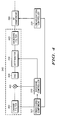
- FIG. 3 is a block diagram representation of a transmitting unit.
- FIG. 4 is a block diagram representation of a baseband component associated with the transmitting unit.
- FIG. 5 is a block diagram representation of a radio frequency (RF) component associated with the transmitting unit.
- RF radio frequency
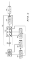
- FIG. 6 is a block diagram representation of the transmitting unit adapted to operate in a manner as described herein.
- FIG. 7 is a block diagram representation of the transmitting unit adapted to operate in a manner as described herein.
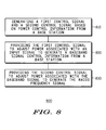
- FIG. 8 is a flow diagram illustrating a method for controlling transmission power associated with a transmitting unit.
- a base station provides power control information to a mobile station for transmission of a radio frequency (RF) signal.
- the mobile station generally includes a transmitting unit operable to generate the radio frequency signal based on an input signal and a baseband signal.
- the transmitting unit may be operable in accordance with a variety of wireless communication protocols such as, but not limited to, a code division multiple access (CDMA) based communication protocol, a time division multiple access (TDMA) based communication protocol, a global service for mobile communications (GSM) based communication protocol, a Bluetooth based communication protocol, and a wireless local area network (WLAN) communication protocol (e.g., an Institute of Electrical and Electronics Engineer (IEEE) 802.11 based communication protocol).
- the transmitting unit may include, but is not limited to, a variable baseband source, a radio frequency (RF) component, a power amplifier, a processing component, a baseband controller, and a linearization controller.
- RF radio frequency
- the variable baseband source is operatively coupled to the processing component and the baseband controller.
- the variable baseband source is operable to generate a baseband signal based on an input signal from the processing component.
- the variable baseband source may include, but is not limited to, a digital multiplier operatively coupled to the processing component, a digital-to-analog converter operatively coupled to the digital multiplier, an attenuator (e.g., a programmable baseband step attenuator) operatively coupled to the digital-to-analog converter and the baseband controller, and a baseband filter operatively coupled to the attenuator and the RF component.
- the variable baseband source may also include a channel filter (e.g., a finite impulse response (FIR) filter) operatively coupled to the processing component and the digital multiplier.
- FIR finite impulse response
- the RF component Operatively coupled to the variable baseband source is the RF component.
- the RF component is operable to generate the RF signal based on the output of the variable baseband source, i.e., the baseband signal.
- the RF component may include, but is not limited to, an RF mixer operatively coupled to the variable baseband source, a variable gain amplifier component operatively coupled to the RF mixer and the linearization controller, and an interstage filter operatively coupled to the variable gain amplifier component and the power amplifier.
- the variable gain amplifier component may include a post-mixer amplifier, a first voltage controlled amplifier (VCA), and a second voltage controlled amplifier (VCA), which are operatively coupled to the linearization controller.
- the second VCA may be operatively coupled to the processing component.
- the processing component is operatively coupled to the variable baseband source and the RF component. That is, the processing component may synchronously adjust the baseband and RF controls of the transmitting unit to change the RF output power.
- the processing component may reduce the input power and the bias level (e.g., current or voltage) associated with the transmitting unit.
- the processing component may generate a first control signal and a second control signal based on power control information from the base station.
- the processing component may provide the first control signal to the baseband controller which, in turn, may adjust the variable baseband source based on the first control signal.
- the baseband controller may reduce power associated with the input signal to generate the baseband signal (i.e., input power).
- the processing component may provide the second control signal to the linearization controller which, in turn, may adjust the radio frequency (RF) component based on the second control signal.
- the linearization controller may reduce power associated with the baseband signal to generate the radio frequency (RF) signal. That is, the second control signal may be used to adjust the bias level of the RF component to adjust the gain/attenuation of the RF signal. Accordingly, reductions in power associated with the input signal and the baseband signal may reduce the amount of supply current demanded by the mobile station. As a result, transmission time of a battery powering mobile station (i.e., battery life) may be extended because the amount of supply current may be reduced as the RF output power is backed off.
- a communication system is also described, and particularly, in terms of a wireless communication system operating in accordance with at least one of several standards.
- These standards include analog, digital or dual-mode communication system protocols such as, but not limited to, the Advanced Mobile Phone System (AMPS), the Narrowband Advanced Mobile Phone System (NAMPS), the Global System for Mobile Communications (GSM), the IS-55 Time Division Multiple Access (TDMA) digital cellular, the IS-95 Code Division Multiple Access (CDMA) digital cellular, CDMA 2000, the Personal Communications System (PCS), 3G, the Universal Mobile Telecommunications System (UMTS) and variations and evolutions of these protocols.
- AMPS Advanced Mobile Phone System
- NAMPS Narrowband Advanced Mobile Phone System
- GSM Global System for Mobile Communications
- TDMA Time Division Multiple Access
- CDMA Code Division Multiple Access
- CDMA 2000 Code Division Multiple Access 2000
- PCS Personal Communications System
- 3G the Universal Mobile Telecommunications System
- UMTS Universal Mobile Telecommunications System
- a wireless communication system 100 includes a communication network 110, and a plurality of base station controllers (BSC), generally shown as 120 and 122, servicing a total service area 130.
- the wireless communication system 100 may be, but is not limited to, a frequency division multiple access (FDMA) based communication system, a time division multiple access (TDMA) based communication system, and code division multiple access (CDMA) based communication system.
- FDMA frequency division multiple access
- TDMA time division multiple access
- CDMA code division multiple access
- each BSC 120 and 122 has associated therewith a plurality of base stations (BS), generally shown as 140, 142, 144, and 146, servicing communication cells, generally shown as 150, 152, 154, and 156, within the total service area 130.
- BS base stations
- the BSCs 120 and 122, and base stations 140, 142, 144, and 146 are specified and operate in accordance with the applicable standard or standards for providing wireless communication services to mobile stations (MS), generally shown as 160, 162, 164, and 166, operating in communication cells 150, 152, 154, and 156, and each of these elements are commercially available from Motorola, Inc. of Schaumburg, Illinois.
- MS mobile stations
- a base station may provide the mobile stations with power control information.
- the power control information may specify the transmission power to be generated by a transmitting unit of a mobile station (i.e., RF output power).
- the base station 142 may provide the mobile station 162 with power control information so that the mobile station 162 may transmit to the base station 142 without causing interference to other mobile stations serviced by the base station 142 such as mobile station 164.
- the mobile station 162 may be operable to control its transmission power and improve on its transmission efficiency.
- the mobile station 162 may be adapted in accordance with a preferred embodiment of the invention to control transmission power associated with a transmitting unit.
- the mobile station 162 generally includes a controller 210, a transmitting unit 220 and a receiving unit 225.
- the controller 210 generally includes a processor 230 and a memory 240.
- the processor 230 is operatively coupled to the memory 240, which stores a program or a set of operating instructions for the processor 230. Accordingly, the processor 230 executes the program or the set of operating instructions such that the mobile station 162 operates in accordance with a preferred embodiment of the invention.
- the program or set of operating instructions may be embodied in a computer-readable medium such as, but not limited to, paper, a programmable gate array, an application specific integrated circuit (ASIC), an erasable programmable read only memory (EPROM), a read only memory (ROM), a random access memory (RAM), a magnetic media, and an optical media.
- a computer-readable medium such as, but not limited to, paper, a programmable gate array, an application specific integrated circuit (ASIC), an erasable programmable read only memory (EPROM), a read only memory (ROM), a random access memory (RAM), a magnetic media, and an optical media.
- the receiving unit 225 is operatively coupled to the controller 210 and an antenna 250.
- the transmitting unit 220 is also operatively coupled to the controller 210 and the antenna 250.
- the transmitting unit 220 generally includes a processing component 310, a baseband controller 320, a linearization controller 330, a variable baseband source 340, and a radio frequency (RF) component 350.
- the processing component 310 is operatively coupled to the baseband controller 320, the linearization controller 330, and the variable baseband source 340.
- the processing component 310 may be, but is not limited to, a microprocessor control unit (MCU) for digital signal processing (DSP).
- MCU microprocessor control unit
- DSP digital signal processing
- the baseband controller 320 is operatively coupled to the variable baseband source 340, and the linearization controller 330 is operatively coupled to the RF component 350 as described in further detail below.
- the variable baseband source 340 generally includes a digital multiplier 410, a digital-to-analog converter (DAC) 420, an attenuator 430 (e.g., a programmable baseband step attenuator), and a baseband filter 440.
- the digital multiplier 410 is operatively coupled to the DAC 420 which, in turn, is operatively coupled to the attenuator 430.
- the attenuator 430 is operatively coupled to the baseband filter 440 and the baseband controller 320.
- the baseband filter 440 is operatively coupled to the RF component 350 as described in further detail below.
- the variable baseband source 340 may also include a channel filter 450 (e.g., a finite impulse response FIR) filter), which is operatively coupled to the processing component 310.
- the channel filter 450 is operatively coupled to the digital multiplier 410 which, in turn, is operatively coupled to the baseband controller 320.
- the variable baseband source 340 is operatively coupled to the RF component 350.
- the RF component 350 generally includes an RF mixer 510, a variable gain amplifier component 520, and an interstage filter 530.
- the baseband filter 440 of the variable baseband source 340 is operatively coupled to the RF mixer 510 which, in turn, is operatively coupled to the variable gain amplifier component 520.
- the variable gain amplifier component 520 may include, but is not limited to, a post-mixer amplifier 542, and a plurality of voltage controlled amplifier (VCA) generally shown as a first VCA 544 and a second VCA 546.
- VCA voltage controlled amplifier
- the linearization controller 330 is operatively coupled to the RF component 350 such that the linearization controller 330 is operable to adjust the variable gain amplifier component 520, i.e., the post-mixer amplifier 542, the first VCA 544, and the second VCA 546. Further, the variable gain amplifier component 520 is operatively coupled to the interstage filter 530.
- the transmitting unit 220 further includes a power amplifier (PA) component 370 and a post-PA component 380.
- PA power amplifier
- the PA component 370 is operatively coupled to the interstage filter 530 of the RF component 350 as shown in FIG. 6 to boost the signal power to the level to be transmitted as one of ordinary skill in the art will readily recognize.
- the post-PA component 380 is operatively coupled to the PA component 370 and the antenna 250.
- the post-PA component 380 may include, but is not limited to, a filter and a switch to prepare a radio frequency signal for transmission via the antenna 250 as one of ordinary skill in the art will readily recognize.
- a basic flow for controlling transmission power associated with a transmitting unit may start the mobile station 162 (e.g., via the receiving unit 225) receiving power control information from a base station such base station 142 shown in FIG. 1.
- the power control information may specify the transmission power to be generated by the transmitting unit 220 of the mobile station 162 (i.e., RF output power).
- the power control information may include an amount of power to increase or decrease the RF output power based on the quality of an RF signal received by the base station 142 from the mobile station 162.
- the processing component 310 Based on that power control information, the processing component 310 generates a first control signal and a second control signal to satisfy the specified transmission power by the base station 142.
- the first control signal may be a digital form of a control signal whereas the second control signal may be an analog form of the control signal.
- the processing component 310 provides the control signals to the baseband controller 320 and the linearization controller 330 to synchronously adjust the baseband and RF controls, respectively, associated with the transmitting unit 220.
- the processing component 310 provides the first control signal to the baseband controller 320 which, in turn, adjusts the variable baseband source 340 (i.e., to adjust the input power of the transmitting unit 220).
- the processing component 310 provides the second control signal to the linearization controller 330 which, in turn, adjusts the RF component 350 (i.e., to adjust the bias level of the transmitting unit 220).
- a radio frequency signal is based on a baseband signal.
- the processing component 310 may provide an input signal to the variable baseband source 340.
- the input signal may be a digital form of a signal including, but not limited to, voice, data, and multimedia.
- the channel filter 450 which may be a finite impulse response (FIR) filter that operates to limit bandwidth of the input signal to a single channel.
- FIR finite impulse response
- the processing component 310 provides the first control signal to the baseband controller 320 to adjust the variable baseband source 340.
- the baseband controller 320 may generate a first adjustment signal and a second adjustment signal to adjust the digital multiplier 410 (i.e., a digital gain/attenuation stage) and the attenuator 430 (i.e., an analog gain/attenuation stage), respectively, of the variable baseband source 340.
- the digital multiplier 410 provides a scaling factor to adjust the amplitude of the output of the channel filter 450 (i.e., a fine adjustment to the input signal).
- the output of the channel filter 450 may be a signal that is proportional to the input signal from the processing component 310 (e.g., a multiple of the input signal).
- the DAC 420 converts the output of the digital multiplier 410 from a digital form to an analog form.
- the attenuator 430 may adjust the output of the DAC 420 (i.e., a coarse adjustment to an analog form of the input signal) in response to the second adjustment signal from the baseband controller 320.
- the baseband filter 440 e.g., a low-pass filter (LPF)
- LPF low-pass filter
- the RF component 350 is operatively coupled to the variable baseband source 340.
- the variable baseband source 340 may provide the baseband signal to the RF component 350 to generate an RF signal.
- the RF mixer 510 modulates the baseband signal to a higher radio frequency for transmission over the air, i.e., a carrier.
- the variable gain amplifier component 520 receives the output of the RF mixer 510.
- the processing component 310 provides the second control signal to the linearization controller 330 to adjust the variable gain amplifier component 520.
- the processing component 310 may provide the second control signal (e.g., the control signal in analog form) to the linearization controller 330 which, in turn, generates a plurality of adjustment signals to adjust the variable gain amplifier component 520.
- the post-mixer amplifier 542 and the first and second VCAs 544, 546 amplify the output of the RF mixer 510 based on the plurality of adjustment signals generated by the linearization controller 330.
- a first adjustment signal from the linearization controller 330 may adjust the bias level of the post-mixer amplifier 542 (e.g., adjust the voltage or current of the post-mixer amplifier 542).
- a second adjustment signal and a third adjustment signal may adjust the RF level of the RF signal via the first and second VCAs 544, 546, respectively (e.g., adjust the voltage of the first and second VCAs 544, 546 to control the amplitude of the output from the post-mixer amplifier 542).
- the interstage filter 530 selectively sorts the output of the variable gain amplifier component 520 to a desired range of frequencies (i.e., "clean-up" the edges) to produce the RF signal.
- the PA component 370 may boost the signal power of the RF signal to the level to be transmitted while the post-PA component 380 may prepare the RF signal for transmission via an over-the-air channel.
- the processing component 310 may also directly adjust the bias level of the RF component 350.
- the processing component 310 may be operatively coupled to the variable gain amplifier component 520.
- the linearization component 330 may be operatively coupled to the post-mixer amplifier 542 and the first VCA 544 while the processing component 310 may be operatively coupled to the second VCA 546 as shown in FIG. 6.
- the transmitting unit 220 may be entirely DSP-controlled by the processing component 310 (i.e., operate without the baseband controller 320 and the linearization controller 330).
- the processing component 310 may operate as both the baseband controller 320 and the linearization controller 330.
- the processing component 310 may operatively coupled to the variable baseband source 340 and the RF component 350.
- the processing component 310 may be operatively coupled to the digital multiplier 410 and the attenuator 430 of the variable baseband source 340.
- the processing component 310 may be operatively coupled to the variable gain amplifier component 520 to adjust the bias level of the RF component 350.
- the processing component 310 may be operatively coupled to the post-mixer amplifier 542, and the first and second VCAs 544 and 546.
- the transmitting unit 220 may include other modulators and intermediate frequency (IF) components as one of ordinary skill in the art will readily recognize to generate the radio frequency signal based on the baseband signal from the variable baseband source 340.
- the transmitting unit 220 may include an IF component operatively coupled to the variable baseband source 340 and the RF component 350.
- the transmitting unit 220 may be integrated into other electronic devices such as, but not limited to, a cordless telephone, a personal digital assistant (PDA), and a laptop computer. Further, the transmitting unit 220 may be operable in accordance with a variety of wireless communication protocols such as, but not limited to, a code division multiple access (CDMA) based communication protocol, a time division multiple access (TDMA) based communication protocol, a global service for mobile communications (GSM) based communication protocol, a Bluetooth based communication protocol, and a wireless local area network (WLAN) communication protocol (e.g., an Institute of Electrical and Electronics Engineer (IEEE) 802.11 based communication protocol).
- CDMA code division multiple access
- TDMA time division multiple access
- GSM global service for mobile communications
- Bluetooth Bluetooth
- WLAN wireless local area network
- Method 800 begins at step 810, wherein a mobile station generates a first control signal and a second control signal based on power control information from a base station providing communication service to the mobile station.
- the power control information provides information so that the mobile station may be operable in accordance with a wireless communication protocol (e.g., CDMA). Accordingly, the mobile station may adjust the input power and the bias level associated with the transmitting unit to meet the output power and linearity requirements of the wireless communication protocol.
- a wireless communication protocol e.g., CDMA
- the mobile station may synchronously reduce the input power and the bias level associated with the transmitting unit.
- the processing component at step 820 provides the first control signal to adjust power associated with an input signal to generate a baseband signal (i.e., to reduce the input power of the transmitting unit).
- the processing component may provide the first control signal to a baseband controller (e.g., one shown as 320 in FIG. 3) which, in turn, adjusts a variable baseband source associated with the transmitting unit (one shown as 340 in FIG. 3) to generate the baseband signal based on the input signal.
- the processing component provides the second control signal to adjust the power associated with the baseband signal to generate the radio frequency signal (i.e., to reduce the bias level associated with the transmitting unit). That is, the processing component may provide the second signal to a linearization controller (one shown as 330 in FIG. 3) that is operable to adjust a radio frequency component associated with the transmitting unit (one shown 350 in FIG. 3) to generate the radio frequency signal.
- a linearization controller one shown as 330 in FIG. 3
- the mobile station may reduce the amount of supply current required to operate the transmitting unit. As a result of less power consumption by the transmitting unit, transmission efficiency of the mobile station may be improved (e.g., transmission time of a battery powering the mobile station may be extended).
Landscapes
- Engineering & Computer Science (AREA)
- Computer Networks & Wireless Communication (AREA)
- Signal Processing (AREA)
- Transmitters (AREA)
- Mobile Radio Communication Systems (AREA)
- Control Of Eletrric Generators (AREA)
Abstract
Description
- The present disclosure relates to wireless communication systems, and more particularly, to a method and an apparatus for controlling power associated with a transmitting unit.
- A wireless communication system is a complex network of systems and elements. Typical systems and elements include (1) a radio link to mobile stations (e.g., a cellular telephone or a subscriber equipment used to access the wireless communication system), which is usually provided by at least one and typically several base stations, (2) communication links between the base stations, (3) a controller, typically one or more base station controllers or centralized base station controllers (BSC/CBSC), to control communication between and to manage the operation and interaction of the base stations, (4) a switching system, typically including a mobile switching center (MSC), to perform call processing within the system, and (5) a link to the land line, i.e., the public switch telephone network (PSTN) or the integrated services digital network (ISDN).
- A base station subsystem (BSS) or a radio access network (RAN), which typically includes one or more base station controllers and a plurality of base stations, provides all of the radio-related functions. The base station controller provides all the control functions and physical links between the switching system and the base stations. The base station controller is also a high-capacity switch that provides functions such as handover, cell configuration, and control of radio frequency (RF) power in the base stations.
- The base station handles the radio interface to the mobile station. The base station includes the radio equipment (transceivers, antennas, amplifiers, etc.) needed to service each communication cell in the system. A group of base stations is controlled by a base station controller. Thus, the base station controller operates in conjunction with the base station as part of the base station subsystem to provide the mobile station with real-time voice, data, and multimedia services (e.g., a call).
- To ensure that all mobile stations receive proper communication services, the base station typically provides power control information. To illustrate this concept, mobile stations serviced by the base station may be anywhere in the communication cell from right under the antenna of the base station to a couple of miles away from the base station. If all of the mobile stations used the same amount of transmission power (i.e., radio frequency (RF) output power), a mobile station proximate to the base station may cause interference to a mobile station distant from the base station. To mitigate this problem, the base station provides each of the mobile stations with power control information so that the mobile stations may optimally control their transmission power and all signals arrive at the base station at substantially equal power. For example, the base station may instruct a mobile station to operate at a reduced transmission power to avoid causing interference to other mobile stations. In particular, the mobile station may vary its transmission power from a few tens of nanowatts up to the order of one watt (W). To reduce transmission power, the gain of the mobile station may be attenuated by adjusting the bias level of the mobile station (e.g., reducing control voltage of the mobile station). Accordingly, the mobile station demands less supply current which, in turn, reduces the third-order intercept point (IP3) level of the mobile station. In particular, the IP3 level indicates the linearity of an RF signal (i.e., distortion level of the signal) from the mobile station. Therefore, higher IP3 level may result in a more distortion-free RF signal from the mobile station but may also require more supply current (i.e., result in greater power consumption by the mobile station).
- Typically, the supply current of a mobile station is constant (i.e., the input power is constant). However, the third-order intercept point (IP3) level may decrease as the transmission power is reduced. Thus, unless the input power of the mobile station is appropriately reduced as well, inter-modulation distortion may be generated during reduction of transmission power because of an insufficient IP3 level for a given amount of input power. In particular, inter-modulation distortion may cause RF energy to overflow into adjacent and/or alternate channels of a frequency band. That is, the RF energy may exceed the acceptable level specified by a wireless communication protocol that is allowed in the frequency band. As a result, spurious RF emissions and degradation in signal quality may occur during reduction of transmission power.
- Further, the trend in the wireless communication industry is not only to provide small hand-held portable devices but also to provide additional user features and functionality. Thus, one aspect of designing a wireless communication system is to optimize the resources available to the mobile station. That is, one method of improving the availability of resources is to reduce the amount of power consumed by a transmitting unit of the mobile station. By reducing power consumption of a mobile station, transmission time may be extended and/or smaller capacity and size batteries may be used.
- Therefore, a need exist to control transmission power associated with a transmitting unit of a mobile station to improve transmission efficiency during power reduction and to optimize communication resources of a wireless communication system.
- This disclosure will describe several embodiments to illustrate its broad teachings. Reference is also made to the attached drawings.
- FIG. 1 is a block diagram representation of a wireless communication system that may be adapted to operate in a manner as described herein.
- FIG. 2 is a block diagram representation of a mobile station.
- FIG. 3 is a block diagram representation of a transmitting unit.
- FIG. 4 is a block diagram representation of a baseband component associated with the transmitting unit.
- FIG. 5 is a block diagram representation of a radio frequency (RF) component associated with the transmitting unit.
- FIG. 6 is a block diagram representation of the transmitting unit adapted to operate in a manner as described herein.
- FIG. 7 is a block diagram representation of the transmitting unit adapted to operate in a manner as described herein.
- FIG. 8 is a flow diagram illustrating a method for controlling transmission power associated with a transmitting unit.
- A method and an apparatus for controlling transmission power associated with a transmitting unit are described. In a wireless communication system, a base station provides power control information to a mobile station for transmission of a radio frequency (RF) signal. The mobile station generally includes a transmitting unit operable to generate the radio frequency signal based on an input signal and a baseband signal. The transmitting unit may be operable in accordance with a variety of wireless communication protocols such as, but not limited to, a code division multiple access (CDMA) based communication protocol, a time division multiple access (TDMA) based communication protocol, a global service for mobile communications (GSM) based communication protocol, a Bluetooth based communication protocol, and a wireless local area network (WLAN) communication protocol (e.g., an Institute of Electrical and Electronics Engineer (IEEE) 802.11 based communication protocol). In particular, the transmitting unit may include, but is not limited to, a variable baseband source, a radio frequency (RF) component, a power amplifier, a processing component, a baseband controller, and a linearization controller.
- The variable baseband source is operatively coupled to the processing component and the baseband controller. The variable baseband source is operable to generate a baseband signal based on an input signal from the processing component. In particular, the variable baseband source may include, but is not limited to, a digital multiplier operatively coupled to the processing component, a digital-to-analog converter operatively coupled to the digital multiplier, an attenuator (e.g., a programmable baseband step attenuator) operatively coupled to the digital-to-analog converter and the baseband controller, and a baseband filter operatively coupled to the attenuator and the RF component. The variable baseband source may also include a channel filter (e.g., a finite impulse response (FIR) filter) operatively coupled to the processing component and the digital multiplier.
- Operatively coupled to the variable baseband source is the RF component. In particular, the RF component is operable to generate the RF signal based on the output of the variable baseband source, i.e., the baseband signal. The RF component may include, but is not limited to, an RF mixer operatively coupled to the variable baseband source, a variable gain amplifier component operatively coupled to the RF mixer and the linearization controller, and an interstage filter operatively coupled to the variable gain amplifier component and the power amplifier. For example, the variable gain amplifier component may include a post-mixer amplifier, a first voltage controlled amplifier (VCA), and a second voltage controlled amplifier (VCA), which are operatively coupled to the linearization controller. In an alternate embodiment, the second VCA may be operatively coupled to the processing component.
- To control transmission power associated with the transmitting unit (i.e., RF output power), the processing component is operatively coupled to the variable baseband source and the RF component. That is, the processing component may synchronously adjust the baseband and RF controls of the transmitting unit to change the RF output power. During an RF output power reduction (i.e., back-off), for example, the processing component may reduce the input power and the bias level (e.g., current or voltage) associated with the transmitting unit. To illustrate this concept, the processing component may generate a first control signal and a second control signal based on power control information from the base station. In particular, the processing component may provide the first control signal to the baseband controller which, in turn, may adjust the variable baseband source based on the first control signal. For example, the baseband controller may reduce power associated with the input signal to generate the baseband signal (i.e., input power). Likewise, the processing component may provide the second control signal to the linearization controller which, in turn, may adjust the radio frequency (RF) component based on the second control signal. Based on the second control signal, the linearization controller may reduce power associated with the baseband signal to generate the radio frequency (RF) signal. That is, the second control signal may be used to adjust the bias level of the RF component to adjust the gain/attenuation of the RF signal. Accordingly, reductions in power associated with the input signal and the baseband signal may reduce the amount of supply current demanded by the mobile station. As a result, transmission time of a battery powering mobile station (i.e., battery life) may be extended because the amount of supply current may be reduced as the RF output power is backed off.
- A communication system is also described, and particularly, in terms of a wireless communication system operating in accordance with at least one of several standards. These standards include analog, digital or dual-mode communication system protocols such as, but not limited to, the Advanced Mobile Phone System (AMPS), the Narrowband Advanced Mobile Phone System (NAMPS), the Global System for Mobile Communications (GSM), the IS-55 Time Division Multiple Access (TDMA) digital cellular, the IS-95 Code Division Multiple Access (CDMA) digital cellular, CDMA 2000, the Personal Communications System (PCS), 3G, the Universal Mobile Telecommunications System (UMTS) and variations and evolutions of these protocols. As shown in FIG. 1, a
wireless communication system 100 includes acommunication network 110, and a plurality of base station controllers (BSC), generally shown as 120 and 122, servicing atotal service area 130. Thewireless communication system 100 may be, but is not limited to, a frequency division multiple access (FDMA) based communication system, a time division multiple access (TDMA) based communication system, and code division multiple access (CDMA) based communication system. As is known for such systems, eachBSC total service area 130. TheBSCs base stations communication cells - To ensure proper communication services are provided to mobile stations within a communication cell, a base station may provide the mobile stations with power control information. The power control information may specify the transmission power to be generated by a transmitting unit of a mobile station (i.e., RF output power). For example, the
base station 142 may provide themobile station 162 with power control information so that themobile station 162 may transmit to thebase station 142 without causing interference to other mobile stations serviced by thebase station 142 such asmobile station 164. Based on the power control information, themobile station 162 may be operable to control its transmission power and improve on its transmission efficiency. - As shown in FIG. 2, the
mobile station 162 may be adapted in accordance with a preferred embodiment of the invention to control transmission power associated with a transmitting unit. Themobile station 162 generally includes a controller 210, a transmittingunit 220 and a receivingunit 225. The controller 210 generally includes aprocessor 230 and amemory 240. Theprocessor 230 is operatively coupled to thememory 240, which stores a program or a set of operating instructions for theprocessor 230. Accordingly, theprocessor 230 executes the program or the set of operating instructions such that themobile station 162 operates in accordance with a preferred embodiment of the invention. The program or set of operating instructions may be embodied in a computer-readable medium such as, but not limited to, paper, a programmable gate array, an application specific integrated circuit (ASIC), an erasable programmable read only memory (EPROM), a read only memory (ROM), a random access memory (RAM), a magnetic media, and an optical media. - The receiving
unit 225 is operatively coupled to the controller 210 and anantenna 250. The transmittingunit 220 is also operatively coupled to the controller 210 and theantenna 250. Referring to FIG. 3, the transmittingunit 220 generally includes aprocessing component 310, abaseband controller 320, alinearization controller 330, avariable baseband source 340, and a radio frequency (RF)component 350. Theprocessing component 310 is operatively coupled to thebaseband controller 320, thelinearization controller 330, and thevariable baseband source 340. Theprocessing component 310 may be, but is not limited to, a microprocessor control unit (MCU) for digital signal processing (DSP). Thebaseband controller 320 is operatively coupled to thevariable baseband source 340, and thelinearization controller 330 is operatively coupled to theRF component 350 as described in further detail below. - As shown in FIG. 4, the
variable baseband source 340 generally includes adigital multiplier 410, a digital-to-analog converter (DAC) 420, an attenuator 430 (e.g., a programmable baseband step attenuator), and abaseband filter 440. Thedigital multiplier 410 is operatively coupled to theDAC 420 which, in turn, is operatively coupled to theattenuator 430. Theattenuator 430 is operatively coupled to thebaseband filter 440 and thebaseband controller 320. To provide theRF component 350 with the output of thevariable baseband source 340, thebaseband filter 440 is operatively coupled to theRF component 350 as described in further detail below. Thevariable baseband source 340 may also include a channel filter 450 (e.g., a finite impulse response FIR) filter), which is operatively coupled to theprocessing component 310. Thechannel filter 450 is operatively coupled to thedigital multiplier 410 which, in turn, is operatively coupled to thebaseband controller 320. - As noted above, the
variable baseband source 340 is operatively coupled to theRF component 350. Referring to FIG. 5, theRF component 350 generally includes anRF mixer 510, a variablegain amplifier component 520, and aninterstage filter 530. In particular, thebaseband filter 440 of thevariable baseband source 340 is operatively coupled to theRF mixer 510 which, in turn, is operatively coupled to the variablegain amplifier component 520. The variablegain amplifier component 520 may include, but is not limited to, apost-mixer amplifier 542, and a plurality of voltage controlled amplifier (VCA) generally shown as afirst VCA 544 and asecond VCA 546. Accordingly, thelinearization controller 330 is operatively coupled to theRF component 350 such that thelinearization controller 330 is operable to adjust the variablegain amplifier component 520, i.e., thepost-mixer amplifier 542, thefirst VCA 544, and thesecond VCA 546. Further, the variablegain amplifier component 520 is operatively coupled to theinterstage filter 530. - Referring back to FIG. 3, the transmitting
unit 220 further includes a power amplifier (PA)component 370 and apost-PA component 380. In particular, thePA component 370 is operatively coupled to theinterstage filter 530 of theRF component 350 as shown in FIG. 6 to boost the signal power to the level to be transmitted as one of ordinary skill in the art will readily recognize. Thepost-PA component 380 is operatively coupled to thePA component 370 and theantenna 250. Thepost-PA component 380 may include, but is not limited to, a filter and a switch to prepare a radio frequency signal for transmission via theantenna 250 as one of ordinary skill in the art will readily recognize. - A basic flow for controlling transmission power associated with a transmitting unit that may be applied with the preferred embodiment of the present invention shown in FIGs. 2, 3, 4, and 5 may start the mobile station 162 (e.g., via the receiving unit 225) receiving power control information from a base station
such base station 142 shown in FIG. 1. The power control information may specify the transmission power to be generated by the transmittingunit 220 of the mobile station 162 (i.e., RF output power). For example, the power control information may include an amount of power to increase or decrease the RF output power based on the quality of an RF signal received by thebase station 142 from themobile station 162. Based on that power control information, theprocessing component 310 generates a first control signal and a second control signal to satisfy the specified transmission power by thebase station 142. For example, the first control signal may be a digital form of a control signal whereas the second control signal may be an analog form of the control signal. Accordingly, theprocessing component 310 provides the control signals to thebaseband controller 320 and thelinearization controller 330 to synchronously adjust the baseband and RF controls, respectively, associated with the transmittingunit 220. In particular, theprocessing component 310 provides the first control signal to thebaseband controller 320 which, in turn, adjusts the variable baseband source 340 (i.e., to adjust the input power of the transmitting unit 220). Likewise, theprocessing component 310 provides the second control signal to thelinearization controller 330 which, in turn, adjusts the RF component 350 (i.e., to adjust the bias level of the transmitting unit 220). - Typically, a radio frequency signal is based on a baseband signal. Thus, to generate the baseband signal, the
processing component 310 may provide an input signal to thevariable baseband source 340. The input signal may be a digital form of a signal including, but not limited to, voice, data, and multimedia. Thechannel filter 450, which may be a finite impulse response (FIR) filter that operates to limit bandwidth of the input signal to a single channel. As noted above, theprocessing component 310 provides the first control signal to thebaseband controller 320 to adjust thevariable baseband source 340. Based on the first control signal, for example, thebaseband controller 320 may generate a first adjustment signal and a second adjustment signal to adjust the digital multiplier 410 (i.e., a digital gain/attenuation stage) and the attenuator 430 (i.e., an analog gain/attenuation stage), respectively, of thevariable baseband source 340. In response to the first adjustment signal from thebaseband controller 320, thedigital multiplier 410 provides a scaling factor to adjust the amplitude of the output of the channel filter 450 (i.e., a fine adjustment to the input signal). Thus, the output of thechannel filter 450 may be a signal that is proportional to the input signal from the processing component 310 (e.g., a multiple of the input signal). Then, theDAC 420 converts the output of thedigital multiplier 410 from a digital form to an analog form. Theattenuator 430 may adjust the output of the DAC 420 (i.e., a coarse adjustment to an analog form of the input signal) in response to the second adjustment signal from thebaseband controller 320. Accordingly, the baseband filter 440 (e.g., a low-pass filter (LPF)) selectively sorts the output of theattenuator 430 to a desired frequency band (i.e., specific range of frequencies) to produce the baseband signal from thevariable baseband source 340. - As mentioned above, the
RF component 350 is operatively coupled to thevariable baseband source 340. Thus, thevariable baseband source 340 may provide the baseband signal to theRF component 350 to generate an RF signal. In particular, theRF mixer 510 modulates the baseband signal to a higher radio frequency for transmission over the air, i.e., a carrier. Accordingly, the variablegain amplifier component 520 receives the output of theRF mixer 510. Theprocessing component 310 provides the second control signal to thelinearization controller 330 to adjust the variablegain amplifier component 520. For example, theprocessing component 310 may provide the second control signal (e.g., the control signal in analog form) to thelinearization controller 330 which, in turn, generates a plurality of adjustment signals to adjust the variablegain amplifier component 520. Thepost-mixer amplifier 542 and the first andsecond VCAs RF mixer 510 based on the plurality of adjustment signals generated by thelinearization controller 330. In particular, a first adjustment signal from thelinearization controller 330 may adjust the bias level of the post-mixer amplifier 542 (e.g., adjust the voltage or current of the post-mixer amplifier 542). A second adjustment signal and a third adjustment signal may adjust the RF level of the RF signal via the first andsecond VCAs second VCAs interstage filter 530 selectively sorts the output of the variablegain amplifier component 520 to a desired range of frequencies (i.e., "clean-up" the edges) to produce the RF signal. Then, thePA component 370 may boost the signal power of the RF signal to the level to be transmitted while thepost-PA component 380 may prepare the RF signal for transmission via an over-the-air channel. - In an alternate embodiment, the
processing component 310 may also directly adjust the bias level of theRF component 350. In particular, theprocessing component 310 may be operatively coupled to the variablegain amplifier component 520. For example, thelinearization component 330 may be operatively coupled to thepost-mixer amplifier 542 and thefirst VCA 544 while theprocessing component 310 may be operatively coupled to thesecond VCA 546 as shown in FIG. 6. - In another alternate embodiment, the transmitting
unit 220 may be entirely DSP-controlled by the processing component 310 (i.e., operate without thebaseband controller 320 and the linearization controller 330). Theprocessing component 310 may operate as both thebaseband controller 320 and thelinearization controller 330. Referring to FIG. 7, for example, theprocessing component 310 may operatively coupled to thevariable baseband source 340 and theRF component 350. To adjust the input power of the transmittingunit 220, theprocessing component 310 may be operatively coupled to thedigital multiplier 410 and theattenuator 430 of thevariable baseband source 340. Further, theprocessing component 310 may be operatively coupled to the variablegain amplifier component 520 to adjust the bias level of theRF component 350. Theprocessing component 310 may be operatively coupled to thepost-mixer amplifier 542, and the first and second VCAs 544 and 546. - In yet another alternate embodiment, the transmitting
unit 220 may include other modulators and intermediate frequency (IF) components as one of ordinary skill in the art will readily recognize to generate the radio frequency signal based on the baseband signal from thevariable baseband source 340. For example, the transmittingunit 220 may include an IF component operatively coupled to thevariable baseband source 340 and theRF component 350. - In addition to operating within a mobile station (e.g., a cellular telephone), the transmitting
unit 220 may be integrated into other electronic devices such as, but not limited to, a cordless telephone, a personal digital assistant (PDA), and a laptop computer. Further, the transmittingunit 220 may be operable in accordance with a variety of wireless communication protocols such as, but not limited to, a code division multiple access (CDMA) based communication protocol, a time division multiple access (TDMA) based communication protocol, a global service for mobile communications (GSM) based communication protocol, a Bluetooth based communication protocol, and a wireless local area network (WLAN) communication protocol (e.g., an Institute of Electrical and Electronics Engineer (IEEE) 802.11 based communication protocol). - In accordance with the preferred embodiments of the present invention, and with references to FIG. 8, a
method 800 for controlling transmission power associated with a transmitting unit of a mobile station is shown.Method 800 begins atstep 810, wherein a mobile station generates a first control signal and a second control signal based on power control information from a base station providing communication service to the mobile station. The power control information provides information so that the mobile station may be operable in accordance with a wireless communication protocol (e.g., CDMA). Accordingly, the mobile station may adjust the input power and the bias level associated with the transmitting unit to meet the output power and linearity requirements of the wireless communication protocol. During an RF output power reduction as specified by the base station, for example, the mobile station may synchronously reduce the input power and the bias level associated with the transmitting unit. In particular, the processing component atstep 820 provides the first control signal to adjust power associated with an input signal to generate a baseband signal (i.e., to reduce the input power of the transmitting unit). For example, the processing component may provide the first control signal to a baseband controller (e.g., one shown as 320 in FIG. 3) which, in turn, adjusts a variable baseband source associated with the transmitting unit (one shown as 340 in FIG. 3) to generate the baseband signal based on the input signal. Likewise atstep 830, the processing component provides the second control signal to adjust the power associated with the baseband signal to generate the radio frequency signal (i.e., to reduce the bias level associated with the transmitting unit). That is, the processing component may provide the second signal to a linearization controller (one shown as 330 in FIG. 3) that is operable to adjust a radio frequency component associated with the transmitting unit (one shown 350 in FIG. 3) to generate the radio frequency signal. By reducing the input power and the bias level during an RF output power reduction, the mobile station may reduce the amount of supply current required to operate the transmitting unit. As a result of less power consumption by the transmitting unit, transmission efficiency of the mobile station may be improved (e.g., transmission time of a battery powering the mobile station may be extended). - Many changes and modifications to the embodiments described herein could be made. The scope of some changes is discussed above. The scope of others will become apparent from the appended claims.
Claims (10)
- In a wireless communication system, wherein a mobile station includes a transmitting unit operable to generate a radio frequency signal based on an input signal and a baseband signal, a method for controlling power associated with the transmitting unit, the method characterized in that it comprises the steps of:generating (810) a first control signal and a second control signal based on power control information;adjusting (820) a level in a variable baseband circuit (340) responsive to the first control signal to adjust the power of a baseband signal generated responsive to the input signal; andadjusting (830) a level in a radio frequency circuit (350) responsive to the second control signal to adjust the power of a radio frequency signal generated responsive to the baseband signal.
- The method as defined in claim 1, further characterized in that the step of generating a first control signal and a second control signal based on power control information generates the control signal based upon power control information received from a base station.
- The method of claim 2, further characterized in that the step of generating a first control signal and a second control signal based on power control information from a base station comprises generating a first control signal and a second control signal based on information associated with radio frequency (RF) output power reduction from a base station.
- The method according to any one of claims 1-3, further characterized in that the step of adjusting a level in a variable baseband circuit responsive to the first control signal comprises reducing the power associated with an input signal to generate a baseband signal.
- The method of claim 4, further characterized in that the step of adjusting a level in a radio frequency circuit responsive to the second control signal includes controlling a linearization controller (330) to adjust power associated with the baseband signal to generate the radio frequency signal.
- The method of any one of claims 1-3, further characterized in that the step of adjusting a level in a radio frequency circuit responsive to the second control signal comprises adjusting the bias level associated with the radio frequency signal.
- The method of any one of claim 1-3, further characterized in that the step of adjusting a level in a radio frequency circuit responsive to the second control signal incldues substantially synchronously adjusting the bias level associated with the radio frequency signal when adjusting power associated with the base band signal.
- In a wireless device, a transmitting unit characterized in that it comprises:variable baseband circuitry (340) operable to generate a baseband signal associated with an input signal;radio frequency circuitry (350) operatively coupled to the variable baseband circuitry, the radio frequency circuitry operable to generate a radio frequency signal associated with the baseband signal; andprocessor circuitry (330) operatively coupled to the variable baseband circuitry and the radio frequency circuitry, the processing circuitry operable to control the baseband circuitry and radio frequency circuitry to adjust the power associated with the baseband signal and the power associated with the radio frequency signal.
- The transmitting unit of claim 8, further characterized in that the processing circuitry is operable to generate a first control signal applied to the baseband circuitry and a second control signal to substantially synchronously adjust the power associated with the baseband signal and the radio frequency signal.
- The transmitting unit according to any one of claims 8 and 9, further characterized in that the radio frequency circuitry includes a linearization controller (330) operatively coupled to the processing circuitry and the radio frequency circuitry, the linearization controller being operable to adjust the radio frequency signal responsive to the second control signal.
Applications Claiming Priority (2)
| Application Number | Priority Date | Filing Date | Title |
|---|---|---|---|
| US10/141,331 US7151947B2 (en) | 2002-05-08 | 2002-05-08 | Method and apparatus for controlling transmission power associated with a transmitting unit |
| US141331 | 2002-05-08 |
Publications (2)
| Publication Number | Publication Date |
|---|---|
| EP1361674A1 true EP1361674A1 (en) | 2003-11-12 |
| EP1361674B1 EP1361674B1 (en) | 2006-03-01 |
Family
ID=29249810
Family Applications (1)
| Application Number | Title | Priority Date | Filing Date |
|---|---|---|---|
| EP03009919A Expired - Lifetime EP1361674B1 (en) | 2002-05-08 | 2003-04-30 | Method and apparatus for controlling power associated with a transmitting unit |
Country Status (9)
| Country | Link |
|---|---|
| US (1) | US7151947B2 (en) |
| EP (1) | EP1361674B1 (en) |
| JP (1) | JP2004166199A (en) |
| KR (1) | KR100524342B1 (en) |
| CN (1) | CN1250023C (en) |
| AT (1) | ATE319234T1 (en) |
| DE (1) | DE60303703T2 (en) |
| ES (1) | ES2259398T3 (en) |
| TW (1) | TWI288535B (en) |
Cited By (1)
| Publication number | Priority date | Publication date | Assignee | Title |
|---|---|---|---|---|
| EP1883167A1 (en) * | 2006-07-26 | 2008-01-30 | Huawei Technologies Co., Ltd. | A system and method for power control, and a remote radio unit |
Families Citing this family (16)
| Publication number | Priority date | Publication date | Assignee | Title |
|---|---|---|---|---|
| US20040176914A1 (en) * | 2001-04-13 | 2004-09-09 | Biosite Incorporated | Methods and compositions for measuring biologically active natriuretic peptides and for improving their therapeutic potential |
| US7333462B2 (en) * | 2002-07-26 | 2008-02-19 | Broadcom Corporation | Wireless terminal operations within wireless local area network |
| DE10250612B4 (en) * | 2002-10-30 | 2014-01-16 | Advanced Micro Devices, Inc. | Automatic power level control circuit for a transceiver |
| JP2006526916A (en) * | 2003-05-09 | 2006-11-24 | コーニンクレッカ フィリップス エレクトロニクス エヌ ヴィ | Method and apparatus for setting transmission power of a mobile communication device |
| EP1673873A1 (en) * | 2003-10-10 | 2006-06-28 | Koninklijke Philips Electronics N.V. | Power saving in a transmitter |
| US7177370B2 (en) * | 2003-12-17 | 2007-02-13 | Triquint Semiconductor, Inc. | Method and architecture for dual-mode linear and saturated power amplifier operation |
| US7366484B2 (en) * | 2004-06-04 | 2008-04-29 | Skyworks Solutions, Inc. | Systems and methods for adjusting the bias level of a mixer in a transmitter |
| WO2008085181A1 (en) * | 2007-01-12 | 2008-07-17 | E28 Limited | Method of controlling an end-user device in communication with a plurality of wireless networks |
| US8325671B2 (en) * | 2007-09-06 | 2012-12-04 | Qualcomm Incorporated | Methods and apparatus for improved utilization of air link resources in a wireless communications system including a multi-antenna element base station |
| KR101436047B1 (en) * | 2007-12-18 | 2014-09-01 | 삼성전자주식회사 | Apparatus and method for reducing bit for digial to analog conversion in frequency division multiple access system |
| US8984105B2 (en) | 2008-05-27 | 2015-03-17 | Qualcomm Incorporated | FMC architecture for CDMA network |
| US8781411B2 (en) * | 2012-01-18 | 2014-07-15 | Qualcomm Incorporated | Baseband filter and upconverter with configurable efficiency for wireless transmitters |
| CN103748933B (en) | 2012-08-17 | 2018-09-07 | 华为终端(东莞)有限公司 | A kind of method and wireless terminal reducing wireless terminal device power consumption |
| CN112152685B (en) | 2020-09-28 | 2022-02-01 | 展讯通信(上海)有限公司 | Site, AP, channel state information feedback, beam forming method and storage medium |
| CN112636790B (en) * | 2020-12-14 | 2023-08-11 | 努比亚技术有限公司 | Electronic price tag communication system, electronic price tag communication method and computer readable storage medium |
| US20240297628A1 (en) * | 2023-03-03 | 2024-09-05 | Skyworks Solutions, Inc. | Rf power amplification apparatus |
Citations (4)
| Publication number | Priority date | Publication date | Assignee | Title |
|---|---|---|---|---|
| US5590411A (en) * | 1995-01-10 | 1996-12-31 | Nokia Mobile Phones Ltd. | Method and apparatus for suppressing spurious third-order responses in transceivers |
| US5862460A (en) * | 1996-09-13 | 1999-01-19 | Motorola, Inc. | Power control circuit for a radio frequency transmitter |
| WO1999030426A1 (en) * | 1997-12-09 | 1999-06-17 | Qualcomm Incorporated | Programmable linear receiver |
| GB2344007A (en) * | 1998-11-04 | 2000-05-24 | Ericsson Inc | Transmission power control for a mobile terminal using received signal strength, base station commands and calibration information in both if and rf sections |
Family Cites Families (3)
| Publication number | Priority date | Publication date | Assignee | Title |
|---|---|---|---|---|
| GB2343588A (en) * | 1998-11-06 | 2000-05-10 | Nokia Mobile Phones Ltd | Transmission power setting in a radio terminal |
| GB2349522A (en) | 1999-04-28 | 2000-11-01 | Nokia Mobile Phones Ltd | Transmit power level control in a mobile telephone |
| US6587511B2 (en) * | 2001-01-26 | 2003-07-01 | Intel Corporation | Radio frequency transmitter and methods thereof |
-
2002
- 2002-05-08 US US10/141,331 patent/US7151947B2/en not_active Expired - Lifetime
-
2003
- 2003-04-30 ES ES03009919T patent/ES2259398T3/en not_active Expired - Lifetime
- 2003-04-30 DE DE60303703T patent/DE60303703T2/en not_active Expired - Lifetime
- 2003-04-30 TW TW092110172A patent/TWI288535B/en not_active IP Right Cessation
- 2003-04-30 EP EP03009919A patent/EP1361674B1/en not_active Expired - Lifetime
- 2003-04-30 AT AT03009919T patent/ATE319234T1/en not_active IP Right Cessation
- 2003-05-06 KR KR10-2003-0028548A patent/KR100524342B1/en not_active Expired - Fee Related
- 2003-05-08 JP JP2003130339A patent/JP2004166199A/en active Pending
- 2003-05-08 CN CNB03130964XA patent/CN1250023C/en not_active Expired - Fee Related
Patent Citations (4)
| Publication number | Priority date | Publication date | Assignee | Title |
|---|---|---|---|---|
| US5590411A (en) * | 1995-01-10 | 1996-12-31 | Nokia Mobile Phones Ltd. | Method and apparatus for suppressing spurious third-order responses in transceivers |
| US5862460A (en) * | 1996-09-13 | 1999-01-19 | Motorola, Inc. | Power control circuit for a radio frequency transmitter |
| WO1999030426A1 (en) * | 1997-12-09 | 1999-06-17 | Qualcomm Incorporated | Programmable linear receiver |
| GB2344007A (en) * | 1998-11-04 | 2000-05-24 | Ericsson Inc | Transmission power control for a mobile terminal using received signal strength, base station commands and calibration information in both if and rf sections |
Cited By (2)
| Publication number | Priority date | Publication date | Assignee | Title |
|---|---|---|---|---|
| EP1883167A1 (en) * | 2006-07-26 | 2008-01-30 | Huawei Technologies Co., Ltd. | A system and method for power control, and a remote radio unit |
| CN101548477B (en) * | 2006-07-26 | 2013-08-07 | 华为技术有限公司 | System and method for power adjustment of remote radio frequency unit and remote radio frequency unit |
Also Published As
| Publication number | Publication date |
|---|---|
| EP1361674B1 (en) | 2006-03-01 |
| CN1457204A (en) | 2003-11-19 |
| DE60303703D1 (en) | 2006-04-27 |
| JP2004166199A (en) | 2004-06-10 |
| TW200402205A (en) | 2004-02-01 |
| ATE319234T1 (en) | 2006-03-15 |
| CN1250023C (en) | 2006-04-05 |
| US7151947B2 (en) | 2006-12-19 |
| TWI288535B (en) | 2007-10-11 |
| DE60303703T2 (en) | 2006-09-07 |
| ES2259398T3 (en) | 2006-10-01 |
| KR20030087546A (en) | 2003-11-14 |
| US20040203983A1 (en) | 2004-10-14 |
| KR100524342B1 (en) | 2005-11-01 |
Similar Documents
| Publication | Publication Date | Title |
|---|---|---|
| EP1361674B1 (en) | Method and apparatus for controlling power associated with a transmitting unit | |
| US7539466B2 (en) | Amplifier with varying supply voltage and input attenuation based upon supply voltage | |
| EP1755214B1 (en) | RF power amplifier for wireless communication apparatus | |
| US7852968B2 (en) | Method and apparatus for optimizing transmitter power efficiency | |
| US6693974B2 (en) | Adaptive digital pre-distortion circuit using adjacent channel power profile and method of operation | |
| US20050287965A1 (en) | Low current direct conversion transmitter architecture | |
| CA2199482A1 (en) | Spread spectrum radiotelephone having adaptive transmitter gain control | |
| JP4511353B2 (en) | Method for optimizing operating point of power amplifier of portable terminal and portable communication terminal | |
| US20020019218A1 (en) | Radiotelephone terminal transmitter and corresponding terminal | |
| US7412216B2 (en) | Radio transmitter | |
| JP2000013246A (en) | Transmitter with multiple modulation schemes | |
| US20060135095A1 (en) | System for controlling power on a mobile station and supporting method and apparatus | |
| HK1080228B (en) | Method and apparatus for optimizing transmitter power efficiency |
Legal Events
| Date | Code | Title | Description |
|---|---|---|---|
| PUAI | Public reference made under article 153(3) epc to a published international application that has entered the european phase |
Free format text: ORIGINAL CODE: 0009012 |
|
| AK | Designated contracting states |
Kind code of ref document: A1 Designated state(s): AT BE BG CH CY CZ DE DK EE ES FI FR GB GR HU IE IT LI LU MC NL PT RO SE SI SK TR |
|
| AX | Request for extension of the european patent |
Extension state: AL LT LV MK |
|
| 17P | Request for examination filed |
Effective date: 20040512 |
|
| 17Q | First examination report despatched |
Effective date: 20040611 |
|
| AKX | Designation fees paid |
Designated state(s): AT BE BG CH CY CZ DE DK EE ES FI FR GB GR HU IE IT LI LU MC NL PT RO SE SI SK TR |
|
| GRAP | Despatch of communication of intention to grant a patent |
Free format text: ORIGINAL CODE: EPIDOSNIGR1 |
|
| GRAS | Grant fee paid |
Free format text: ORIGINAL CODE: EPIDOSNIGR3 |
|
| GRAA | (expected) grant |
Free format text: ORIGINAL CODE: 0009210 |
|
| AK | Designated contracting states |
Kind code of ref document: B1 Designated state(s): AT BE BG CH CY CZ DE DK EE ES FI FR GB GR HU IE IT LI LU MC NL PT RO SE SI SK TR |
|
| PG25 | Lapsed in a contracting state [announced via postgrant information from national office to epo] |
Ref country code: IT Free format text: LAPSE BECAUSE OF FAILURE TO SUBMIT A TRANSLATION OF THE DESCRIPTION OR TO PAY THE FEE WITHIN THE PRESCRIBED TIME-LIMIT;WARNING: LAPSES OF ITALIAN PATENTS WITH EFFECTIVE DATE BEFORE 2007 MAY HAVE OCCURRED AT ANY TIME BEFORE 2007. THE CORRECT EFFECTIVE DATE MAY BE DIFFERENT FROM THE ONE RECORDED. Effective date: 20060301 Ref country code: SK Free format text: LAPSE BECAUSE OF FAILURE TO SUBMIT A TRANSLATION OF THE DESCRIPTION OR TO PAY THE FEE WITHIN THE PRESCRIBED TIME-LIMIT Effective date: 20060301 Ref country code: CH Free format text: LAPSE BECAUSE OF FAILURE TO SUBMIT A TRANSLATION OF THE DESCRIPTION OR TO PAY THE FEE WITHIN THE PRESCRIBED TIME-LIMIT Effective date: 20060301 Ref country code: LI Free format text: LAPSE BECAUSE OF FAILURE TO SUBMIT A TRANSLATION OF THE DESCRIPTION OR TO PAY THE FEE WITHIN THE PRESCRIBED TIME-LIMIT Effective date: 20060301 Ref country code: NL Free format text: LAPSE BECAUSE OF FAILURE TO SUBMIT A TRANSLATION OF THE DESCRIPTION OR TO PAY THE FEE WITHIN THE PRESCRIBED TIME-LIMIT Effective date: 20060301 Ref country code: AT Free format text: LAPSE BECAUSE OF FAILURE TO SUBMIT A TRANSLATION OF THE DESCRIPTION OR TO PAY THE FEE WITHIN THE PRESCRIBED TIME-LIMIT Effective date: 20060301 Ref country code: FI Free format text: LAPSE BECAUSE OF FAILURE TO SUBMIT A TRANSLATION OF THE DESCRIPTION OR TO PAY THE FEE WITHIN THE PRESCRIBED TIME-LIMIT Effective date: 20060301 Ref country code: RO Free format text: LAPSE BECAUSE OF FAILURE TO SUBMIT A TRANSLATION OF THE DESCRIPTION OR TO PAY THE FEE WITHIN THE PRESCRIBED TIME-LIMIT Effective date: 20060301 Ref country code: SI Free format text: LAPSE BECAUSE OF FAILURE TO SUBMIT A TRANSLATION OF THE DESCRIPTION OR TO PAY THE FEE WITHIN THE PRESCRIBED TIME-LIMIT Effective date: 20060301 Ref country code: BE Free format text: LAPSE BECAUSE OF FAILURE TO SUBMIT A TRANSLATION OF THE DESCRIPTION OR TO PAY THE FEE WITHIN THE PRESCRIBED TIME-LIMIT Effective date: 20060301 |
|
| REG | Reference to a national code |
Ref country code: GB Ref legal event code: FG4D |
|
| REG | Reference to a national code |
Ref country code: CH Ref legal event code: EP |
|
| REG | Reference to a national code |
Ref country code: IE Ref legal event code: FG4D |
|
| REF | Corresponds to: |
Ref document number: 60303703 Country of ref document: DE Date of ref document: 20060427 Kind code of ref document: P |
|
| PG25 | Lapsed in a contracting state [announced via postgrant information from national office to epo] |
Ref country code: MC Free format text: LAPSE BECAUSE OF NON-PAYMENT OF DUE FEES Effective date: 20060430 |
|
| PG25 | Lapsed in a contracting state [announced via postgrant information from national office to epo] |
Ref country code: IE Free format text: LAPSE BECAUSE OF NON-PAYMENT OF DUE FEES Effective date: 20060502 |
|
| PG25 | Lapsed in a contracting state [announced via postgrant information from national office to epo] |
Ref country code: SE Free format text: LAPSE BECAUSE OF FAILURE TO SUBMIT A TRANSLATION OF THE DESCRIPTION OR TO PAY THE FEE WITHIN THE PRESCRIBED TIME-LIMIT Effective date: 20060601 Ref country code: BG Free format text: LAPSE BECAUSE OF FAILURE TO SUBMIT A TRANSLATION OF THE DESCRIPTION OR TO PAY THE FEE WITHIN THE PRESCRIBED TIME-LIMIT Effective date: 20060601 Ref country code: DK Free format text: LAPSE BECAUSE OF FAILURE TO SUBMIT A TRANSLATION OF THE DESCRIPTION OR TO PAY THE FEE WITHIN THE PRESCRIBED TIME-LIMIT Effective date: 20060601 |
|
| PG25 | Lapsed in a contracting state [announced via postgrant information from national office to epo] |
Ref country code: PT Free format text: LAPSE BECAUSE OF FAILURE TO SUBMIT A TRANSLATION OF THE DESCRIPTION OR TO PAY THE FEE WITHIN THE PRESCRIBED TIME-LIMIT Effective date: 20060801 |
|
| NLV1 | Nl: lapsed or annulled due to failure to fulfill the requirements of art. 29p and 29m of the patents act | ||
| REG | Reference to a national code |
Ref country code: CH Ref legal event code: PL |
|
| REG | Reference to a national code |
Ref country code: ES Ref legal event code: FG2A Ref document number: 2259398 Country of ref document: ES Kind code of ref document: T3 |
|
| ET | Fr: translation filed | ||
| PLBE | No opposition filed within time limit |
Free format text: ORIGINAL CODE: 0009261 |
|
| STAA | Information on the status of an ep patent application or granted ep patent |
Free format text: STATUS: NO OPPOSITION FILED WITHIN TIME LIMIT |
|
| 26N | No opposition filed |
Effective date: 20061204 |
|
| PG25 | Lapsed in a contracting state [announced via postgrant information from national office to epo] |
Ref country code: GR Free format text: LAPSE BECAUSE OF FAILURE TO SUBMIT A TRANSLATION OF THE DESCRIPTION OR TO PAY THE FEE WITHIN THE PRESCRIBED TIME-LIMIT Effective date: 20060602 Ref country code: CZ Free format text: LAPSE BECAUSE OF FAILURE TO SUBMIT A TRANSLATION OF THE DESCRIPTION OR TO PAY THE FEE WITHIN THE PRESCRIBED TIME-LIMIT Effective date: 20060301 |
|
| PG25 | Lapsed in a contracting state [announced via postgrant information from national office to epo] |
Ref country code: EE Free format text: LAPSE BECAUSE OF FAILURE TO SUBMIT A TRANSLATION OF THE DESCRIPTION OR TO PAY THE FEE WITHIN THE PRESCRIBED TIME-LIMIT Effective date: 20060301 |
|
| PG25 | Lapsed in a contracting state [announced via postgrant information from national office to epo] |
Ref country code: LU Free format text: LAPSE BECAUSE OF NON-PAYMENT OF DUE FEES Effective date: 20060430 Ref country code: TR Free format text: LAPSE BECAUSE OF FAILURE TO SUBMIT A TRANSLATION OF THE DESCRIPTION OR TO PAY THE FEE WITHIN THE PRESCRIBED TIME-LIMIT Effective date: 20060301 Ref country code: HU Free format text: LAPSE BECAUSE OF FAILURE TO SUBMIT A TRANSLATION OF THE DESCRIPTION OR TO PAY THE FEE WITHIN THE PRESCRIBED TIME-LIMIT Effective date: 20060902 |
|
| PG25 | Lapsed in a contracting state [announced via postgrant information from national office to epo] |
Ref country code: CY Free format text: LAPSE BECAUSE OF FAILURE TO SUBMIT A TRANSLATION OF THE DESCRIPTION OR TO PAY THE FEE WITHIN THE PRESCRIBED TIME-LIMIT Effective date: 20060301 |
|
| REG | Reference to a national code |
Ref country code: GB Ref legal event code: 732E Free format text: REGISTERED BETWEEN 20110127 AND 20110202 |
|
| REG | Reference to a national code |
Ref country code: DE Ref legal event code: R081 Ref document number: 60303703 Country of ref document: DE Owner name: MOTOROLA MOBILITY, INC. ( N.D. GES. D. STAATES, US Free format text: FORMER OWNER: MOTOROLA, INC., SCHAUMBURG, US Effective date: 20110324 Ref country code: DE Ref legal event code: R081 Ref document number: 60303703 Country of ref document: DE Owner name: MOTOROLA MOBILITY, INC. ( N.D. GES. D. STAATES, US Free format text: FORMER OWNER: MOTOROLA, INC., SCHAUMBURG, ILL., US Effective date: 20110324 |
|
| REG | Reference to a national code |
Ref country code: FR Ref legal event code: TP Owner name: MOTOROLA MOBILITY, INC., US Effective date: 20110912 |
|
| REG | Reference to a national code |
Ref country code: FR Ref legal event code: PLFP Year of fee payment: 13 |
|
| PGFP | Annual fee paid to national office [announced via postgrant information from national office to epo] |
Ref country code: GB Payment date: 20150427 Year of fee payment: 13 Ref country code: DE Payment date: 20150429 Year of fee payment: 13 Ref country code: ES Payment date: 20150427 Year of fee payment: 13 |
|
| PGFP | Annual fee paid to national office [announced via postgrant information from national office to epo] |
Ref country code: FR Payment date: 20150417 Year of fee payment: 13 |
|
| REG | Reference to a national code |
Ref country code: DE Ref legal event code: R119 Ref document number: 60303703 Country of ref document: DE |
|
| GBPC | Gb: european patent ceased through non-payment of renewal fee |
Effective date: 20160430 |
|
| REG | Reference to a national code |
Ref country code: FR Ref legal event code: ST Effective date: 20161230 |
|
| PG25 | Lapsed in a contracting state [announced via postgrant information from national office to epo] |
Ref country code: FR Free format text: LAPSE BECAUSE OF NON-PAYMENT OF DUE FEES Effective date: 20160502 Ref country code: DE Free format text: LAPSE BECAUSE OF NON-PAYMENT OF DUE FEES Effective date: 20161101 Ref country code: GB Free format text: LAPSE BECAUSE OF NON-PAYMENT OF DUE FEES Effective date: 20160430 |
|
| PG25 | Lapsed in a contracting state [announced via postgrant information from national office to epo] |
Ref country code: ES Free format text: LAPSE BECAUSE OF NON-PAYMENT OF DUE FEES Effective date: 20160430 |
|
| REG | Reference to a national code |
Ref country code: ES Ref legal event code: FD2A Effective date: 20180626 |
|
| PG25 | Lapsed in a contracting state [announced via postgrant information from national office to epo] |
Ref country code: ES Free format text: LAPSE BECAUSE OF NON-PAYMENT OF DUE FEES Effective date: 20160501 |