EP1360927B1 - Dispositif d'imagerie optique et procede de detection d'imagerie optique - Google Patents
Dispositif d'imagerie optique et procede de detection d'imagerie optique Download PDFInfo
- Publication number
- EP1360927B1 EP1360927B1 EP02769206A EP02769206A EP1360927B1 EP 1360927 B1 EP1360927 B1 EP 1360927B1 EP 02769206 A EP02769206 A EP 02769206A EP 02769206 A EP02769206 A EP 02769206A EP 1360927 B1 EP1360927 B1 EP 1360927B1
- Authority
- EP
- European Patent Office
- Prior art keywords
- optical
- probe
- imaging system
- optical imaging
- light
- Prior art date
- Legal status (The legal status is an assumption and is not a legal conclusion. Google has not performed a legal analysis and makes no representation as to the accuracy of the status listed.)
- Expired - Lifetime
Links
Images


Classifications
-
- A—HUMAN NECESSITIES
- A61—MEDICAL OR VETERINARY SCIENCE; HYGIENE
- A61B—DIAGNOSIS; SURGERY; IDENTIFICATION
- A61B5/00—Measuring for diagnostic purposes; Identification of persons
- A61B5/68—Arrangements of detecting, measuring or recording means, e.g. sensors, in relation to patient
- A61B5/6846—Arrangements of detecting, measuring or recording means, e.g. sensors, in relation to patient specially adapted to be brought in contact with an internal body part, i.e. invasive
- A61B5/6847—Arrangements of detecting, measuring or recording means, e.g. sensors, in relation to patient specially adapted to be brought in contact with an internal body part, i.e. invasive mounted on an invasive device
- A61B5/6852—Catheters
-
- A—HUMAN NECESSITIES
- A61—MEDICAL OR VETERINARY SCIENCE; HYGIENE
- A61B—DIAGNOSIS; SURGERY; IDENTIFICATION
- A61B5/00—Measuring for diagnostic purposes; Identification of persons
- A61B5/0059—Measuring for diagnostic purposes; Identification of persons using light, e.g. diagnosis by transillumination, diascopy, fluorescence
- A61B5/0062—Arrangements for scanning
- A61B5/0066—Optical coherence imaging
-
- A—HUMAN NECESSITIES
- A61—MEDICAL OR VETERINARY SCIENCE; HYGIENE
- A61B—DIAGNOSIS; SURGERY; IDENTIFICATION
- A61B2562/00—Details of sensors; Constructional details of sensor housings or probes; Accessories for sensors
- A61B2562/08—Sensors provided with means for identification, e.g. barcodes or memory chips
Definitions
- the present invention relates to an optical imaging system and an optical imaging detection method for irradiating low coherence light beam to an object and constructing a tomographic image of the inside of the object from information of light scattered or reflected from the object.
- optical imaging systems include, for example, the one described in Japanese Unexamined Patent Application Publication No. 11-148897 .
- an optical imaging system referred to as an optical coherence tomography system.
- the optical coherence tomography system has an optical probe that is inserted into a human body and that has a light receiving/emitting means incorporated in the distal part thereof.
- the light receiving/emitting means emits low coherence light beam to an object through a light receiving/emitting port and receives light reflected from the object. Based on the reflected light the optical probe receives from the object, a tomographic image of the object is produced by utilizing the interference of light.
- an optical scanner probe is connected to a main body of an observing device through a connector by which the optical scanner probe can be freely detachably attached to the main body.
- the probe can be readily replaced with another.
- Japanese Patent Application No. 11-134590 has disclosed other type of optical imaging system.
- This type of optical imaging system includes a rotational driving means, which rotates an optical scanner probe, and an advancement/withdrawal driving means, which advances or withdraws the optical scanner program in axial directions, so as to produce a three-dimensional tomographic image of an object.
- optical scanner probes that are different from one another in terms of any parameter other than the length thereof (different types of optical scanner probes) are not interchangeable.
- the optical imaging system described in the Japanese Patent Application No. 11-134590 is a dedicated three-dimensional optical imaging system.
- the optical imaging system is therefore little general-purpose.
- an optical scanner probe other than a three-dimensional optical scanner probe is used in combination, it is hard to control the system and display images suitable to the probe therewith.
- the optical imaging system is poor in adaptability.
- the conventional optical imaging systems have not taken measures to obviate the necessity of correcting an individual difference of an optical probe that is freely detachably attached to a main body.
- the conventional optical imaging systems include a scanning means that includes a scanner but do not attempt to control an image producing means using information, which is acquired by the scanning means, in consideration of the characteristics of an optical probe.
- a gain to be produced is controlled based on the property of return light from an object to be observed which is measured in advance. It is therefore necessary to measure the property of return light relative to each probe whose optical characteristics are different from the others. Gain control is therefore labor-intensive.
- a bandwidth is optimally adjusted by observing an object to be observed and by manually adjusting a bandwidth limitation filter. Every time a probe whose optical characteristics are different from references is replaced with another, or every time an object is observed using the same probe, a bandwidth must be regulated. This is bothering.
- a predetermined gamma is calculated in advance relative to an object to be observed. An actual gamma is corrected based on the calculated value. It is therefore necessary to acquire and adjust a gamma every time an optical probe whose optical characteristics are different from references is replaced with another. The gamma control is labor-intensive.
- the conventional optical imaging systems include, for example, like the one described in Japanese Unexamined Patent Application Publication No. 2000-75210 , an optical imaging system having two scanners thereof driven to scan inputs while tracing a Lissajous figure.
- the optical imaging system described in the Japanese Unexamined Patent Application Publication No. 2000-75210 has not taken measures against the conditions for driving the scanners, the details of an operating procedure, and imaging.
- Doument D1 discloses a device as described in the preamble of cl. 1.
- An object of the present invention is to provide an optical imaging system and an optical imaging detection method capable of automatically detecting and identifying the characteristics of any of a plurality of types of optical probes.
- Another object of the present invention is to provide an optical imaging system that automatically detects the characteristics of an optical probe (including a scanning technique, a focal point, and the diameter of a sheath) so as to control the probe optimally to the type of probe or determine a display form optimally thereto. Otherwise, the optical imaging system presents on a display image the information of the type of optical probe or of the characteristics thereof or enables designation of the information thereof.
- an optical imaging system that automatically detects the characteristics of an optical probe (including a scanning technique, a focal point, and the diameter of a sheath) so as to control the probe optimally to the type of probe or determine a display form optimally thereto. Otherwise, the optical imaging system presents on a display image the information of the type of optical probe or of the characteristics thereof or enables designation of the information thereof.
- Still another object of the present invention is to provide an optical imaging system capable of scanning-drive controlling, a light path adjusting, or a display image adjusting, suitable to a connected optical probe.
- JP 05049600 relates to an electronic endoscope apparatus, wherein an image of an object is taken with solid image sensor and is outputted adjusting the level of an output signal of the solid image sensor to an optimum level with an AGC circuit.
- a maximum/minimum gain memory means stores an allowable adjusting range of the output signal for each endoscope.
- a scope judging means judges intrinsic information to each endoscope based on an output of a judgment signal generation means.
- An output signal level of the AGC circuit is evaluated by an image evaluating means and the allowable adjusting range is adjusted corresponding to the endoscope stored in the maximum/minimum memory means based on an output of the image evaluating means by a maximum/minimum gain computing means, a minimum gain control means, a maximum gain control means and an AGC control means and a control is performed to make the AGC circuit operate within the allowable gain adjusting range.
- US 5,048,524 refers to a method and apparatus for measuring the oxygen saturation level and hematocrit of human blood in real time.
- a catheter having a notch in its tip is inserted into a blood vessel and guided to a desired location in the body of a patient. Bursts of light at each of three wavelengths are transmitted through the blood in the notch. The intensities of the bursts of light after transmission are utilized along with a set of molecular extinction coefficients and optical scattering coefficients to calculate the oxygen level and hematocrit.
- the light is provided by a set of LEDs in a housing connected to the catheter and the intensity of the transmitted light is measured by a photocell in the same housing.
- Optical fibres transmit the light through the catheter between the housing and the notch. Characterization resistors in the housing are encoded with characteristics such as the wavelengths of the LEDs and the width of the notch.
- blood circulating through a loop out of the patient's body is passed through a chamber and is exposed to the
- WO 00/42911 relates to a universal/upgrading pulse oximeter (UPO) comprising a portable unit and a dockinig station together providing three-instruments-in-one functionality for measuring oxygen saturation and related physiological parameters.
- the portable unit functions as a handheld pulse oximeter.
- the combination of the docked portable and the docking station functions as a stand-alone, high-performance pulse oximeter.
- the portable-docking station combination is also connectable to, and universally compatible with, pulse oximeters from various manufacturers through use of a waveform generator.
- the UPO provides a universal sensor to pulse oximeter interface and a pulse oximeter measurement capability that upgrades the performance of conventional instruments by increasing low perfusion performance and motion artefact immunity, for example.
- Universal compatibility combined with portability allows the UPO to be transported along with patients transferred between an ambulance and a hospital, or between various hospital sits, providing continuous patient monitoring in addition to plug-compatibility and functional upgrading for multiparameter patient monitoring systems.
- the image on the portable display is rotatable, either manually when undocked or as a function of orientation.
- the docking station can have a web server and network interface that allows UPO data to be downloaded and viewed as web pages over a local area network or the Internet.
- EP 0 748 609 A1 refers to an apparatus characterizing the operating characteristics of a medical monitoring probe. This apparatus not only identifies the present value of a plurality of operating characteristics of the optical components contained in the probe, but also computes the interrelationship therebetween to produce a composite probe indicia that substantially defines the net operating characteristics of the probe, including the interrelation of the various interactive and/or cumulative effects.
- This composite probe indicia represents either a number or a graphical representation of probe operating characteristics that can be used directly by the processor contained within the monitoring system to perform the required computations.
- JP 11148897 relates to an optical imaging apparatus, wherein low interference light, on one side, from a low interference light source is radiated to an organism tissue via an optical scanning probe by a freely detachable connector part from its tip, and the light on the other side is guided to an optical-path-length variable mechanism by a second single mode fibre from a photocoupler in a halfway part.
- the optical-path-length variable mechanism is provided with a galvanometer mirror whose optical path length is changed so as to correspond to a scanning range and with a one-axis stage which changes an optical path length so as to absorb an irregularity in every length of the optical scanning probe.
- the optical path length is adjusted by the one-axis stage so as to be set to a state capable of detecting the interference light in the scanning range, and a tomogram can be obtained surely.
- US 6,193,669 B1 refers to a method and devices for detection, localization and characterization of occlusions, aneurysms, dissections stent position, dissection stent mal-position, wall characteristics and vascular bed.
- the invention is based on introducing an artificial pressure or flow excitation signal (a single signal or more) into the blood vessel (or in other tubular flowing fluid conduits), measurement and analysis of the pressure and or flow.
- an artificial pressure or flow excitation signal a single signal or more
- a method and devices for detection and characterization of partial or total occlusion or aneurysm in blood vessels or in other tubular flowing fluid conduits within a body, such as urine flow in the urethra are described.
- the present invention provides an optical imaging system that irradiates light from a light source and constructs an observed image of an object using information carried by return light from the object.
- the optical imaging system consists mainly of:
- the present invention provides an optical imaging detection method according to which light emanating from a light source is irradiated to an object, and an observed image of the object is constructed using information carried by return light from the object.
- the optical imaging detection method is implemented in an optical imaging system that includes:
- a focal range, a focal position and a numerical aperture of the optical probe being included in the characteristics of the optical probe.
- the conditions for controlling an optical probe are determined based on the characteristics of the optical probe detected by the detecting means.
- Fig. 1 to Fig. 19 are concerned with a first embodiment of the present invention.
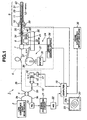
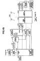
- Fig. 1 shows the configuration of an optical imaging system in accordance with the first embodiment.
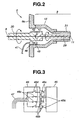
- Fig. 2 shows the structure of a micro-switch-inclusive probe information detecting mechanism included in the optical imaging system shown in Fig. 1 .
- Fig. 3 is an explanatory diagram concerning the principles of operation based on a micro-switch-inclusive detecting method implemented in the mechanism shown in Fig. 2 .
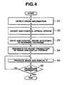
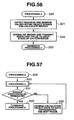
- Fig. 4 is a flowchart describing a procedure for detecting and processing probe information.
- Fig. 5 is a flowchart detailing the probe information detecting procedure mentioned in Fig. 4 .
- Fig. 1 shows the configuration of an optical imaging system in accordance with the first embodiment.
- Fig. 2 shows the structure of a micro-switch-inclusive probe information detecting mechanism included in the optical imaging system shown in Fig. 1 .
- Fig. 3 is an explanatory diagram concerning the
- FIG. 6 is a flowchart describing a procedure of adjusting and controlling an optical system included in the procedure mentioned in Fig. 4 .
- Fig. 7 is a flowchart describing a procedure of driving and controlling a probe according to a scanning technique implemented in the probe, a procedure of imaging, and a procedure of determining the settings for display, which correspond to steps described in Fig. 4 .
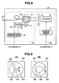
- Fig. 8 shows the structure of an optical path length automatic adjustment mechanism that adjusts the optical path length of reference light and that is included in an optical path length scanning unit.
- Fig. 9A and Fig. 9B show radial-scan tomographic images produced by performing radial scanning before and after the optical path length automatic adjustment mechanism shown in Fig. 8 is actuated.
- Fig. 9A and Fig. 9B show radial-scan tomographic images produced by performing radial scanning before and after the optical path length automatic adjustment mechanism shown in Fig. 8 is actuated.
- FIG. 10 shows the structure of an optical probe whose sheath has a small diameter.
- Fig. 11 shows the structure of an optical probe whose sheath has a large diameter.
- Fig. 12 is an explanatory diagram showing an image displayed on the optical imaging system shown in Fig. 10.
- Fig. 13 is an explanatory diagram showing the sheath of the optical probe shown in Fig. 11 on a radial-scan tomographic image with an optical path length unadjusted.
- Fig. 14 is an explanatory diagram showing the sheath of the optical probe shown in Fig. 11 on a radial-scan tomographic image with an optical path length adjusted.
- Fig. 11 shows the structure of an optical probe whose sheath has a small diameter.
- Fig. 11 shows the structure of an optical probe whose sheath has a large diameter.
- Fig. 12 is an explanatory diagram showing an image displayed on the optical imaging system shown in Fig. 10.
- Fig. 13 is an
- Fig. 15 is an explanatory diagram showing a focal point of measurement light beam, which is propagated from an optical probe, and a focal range thereof.
- Fig. 16 is an explanatory diagram showing a focal point offered by an optical probe and delineated in a radial-scan OCT image.
- Fig. 17 is an explanatory diagram showing a focal point offered by an optical probe and delineated in a linear-scan OCT image.
- Fig. 18 is an explanatory diagram showing a focal range offered by an optical probe and delineated in a radial-scan OCT image.
- Fig. 19 is an explanatory diagram showing a focal range offered by an optical probe and delineated in a linear-scan OCT image.
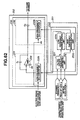
- An optical imaging system (optical tomographic imaging system) 1 shown in Fig. 1 includes a low coherence light beam source 2.
- the low coherence light beam source 2 generates low coherence light beam whose wavelength is, for example, 1300 nm and whose coherence length is, for example, about 17 ⁇ m, that is, low coherence light beam that exhibits coherence within a short distance. For example, assume that the light beam is bisected and then merged again. If a difference between two optical path lengths to a point of bisection is a short distance of about 17 ⁇ m, the light is detected as coherent light beam. If the difference exceeds about 17 ⁇ m, the light exhibits incoherence.
- the first single-mode fiber 3a is optically coupled with a second single-mode fiber 5a within an optical coupler 4.
- the optical coupler 4 bisects light into measurement light beam and reference light.
- the measurement light beam is transmitted to a third single-mode fiber 3b, while the reference light is transmitted to a fourth single-mode fiber 5b.
- the distal end of the third single-mode fiber 3b (coupled to the optical coupler 4) is joined with a fifth single-mode fiber 8 via an optical rotary joint 7, which has non-rotating and rotating sections and passes light, within an optical imaging observation device 6.
- a connector (or attachment) 10 of an optical scanner probe (hereinafter abbreviated to an optical probe) 9 is freely detachably attached to the distal end of the fifth single-mode fiber 8.
- the light emanating from the low coherence light beam source 2 is transmitted to a sixth single-mode fiber 11 that runs through the optical scanner probe 9.
- the transmitted measurement light beam is reflected from a prism 43 incorporated in the distal part of the optical probe 9, and irradiated to a living-body tissue 12 that is an object while being scanned.
- the reference light separated by the optical coupler 4 and propagated along the fourth single-mode fiber 5b is transmitted to an optical path length scanning unit 13 that changes the optical path length of the reference light.
- the reference light is irradiated to a mirror 15 via a lens 14 from the distal end surface of the optical fiber 5b within the optical path length scanning unit 13, and then reflected from it.
- the mirror 15 can be advanced or withdrawn in optical-axis directions by means of an actuator 16. By changing the position of the mirror 15, the optical path length (optical delay) can be varied.
- the action of the actuator 16 is controlled by an actuator control circuit 17 connected to a computer 18.
- the optical path length scanning unit 13 can change with high speed the optical path length of the reference light within the scanning range by the optical probe 9, in relative to a predetermined scanning range extending in the direction of depth of the living-body tissue 12.
- part of the measurement light beam scattered or reflected from the surface of the living-body tissue 12 or internally thereof is fetched into the optical probe 9 and returned to the third single-mode fiber 3b by reversely tracing the light path.
- the reference return light from the optical path length scanning unit 13 returns to the fourth single-mode fiber 5b.
- the return light of the measurement light beam and the reference light interfere with each other within the optical coupler 4, and the resultant light is incident on a photo-detector (PD) 19 through the distal end of the second single-mode fiber 5a.
- PD photo-detector
- a coherence electric signal resulting from photoelectric conversion performed by the photo-detector 19 is inputted to a signal processing circuit 21.
- the signal processing circuit 21 processes the coherence electric signal.
- the output of the signal processing circuit 21 is transmitted to the computer 18 via an A/D converter 22.
- the computer 18 produces image data representing a tomographic image, and transmits the image data to a monitor 23. Consequently, an OCT (image produced by optical imaging) image 30 is displayed on a display surface 23a of the monitor.
- the optical rotary joint 7 is driven by a drive unit 24 included in the observing device 6.
- the drive unit 24 includes rotational driving means 25 that rotationally drives the rotor included in the optical rotary joint 7, and an advancing/withdrawing means 27 that advances or withdraws the optical rotary joint 7 and rotational driving means 25, which are mounted on a lock mount 26, in axial directions.
- the rotational driving means 25 and advancing/withdrawing means 27 are controlled by a driving control circuit 28.
- a light guide member (a hollow flexible shaft 29 having the optical fiber 11 run through it) included in the probe 9 and joined with the rotor included in the optical rotary joint 7 radially rotates or linearly advances or withdraws within a sheath 31 of the optical probe 9.
- the rotational driving means 25 consists of a motor 32 that rotates for driving, a motor rotor (pulley) 33 fixed to the rotation shaft of the motor 32, and a belt 34 laid over between the motor rotor (pulley) 33 and a shaft 20 through which the fifth single-mode fiber 8 runs.
- the advancing/withdrawing means 27 consists of a motor 35 that rotates for driving, a rotary plate 36 that is rotated by the motor 35, and a driving rod 37 having one end thereof coupled to the rotary plate 36, having the other end thereof coupled to the lock mount 26, and being used to advance or withdraw the assemblage coupled to the other end thereof.
- the computer 18 controls the rotational driving means 25 and advancing/withdrawing means 27, which are included in the driving unit 24, via the driving control circuit 28.
- Probe information specifying means 38 that specifies feature information concerning the optical probe 9 is connected to the computer 18.
- the probe information specifying means 38 is used to enter the feature information of the optical probe 9, whereby the computer 18 can control or perform adjustment or adjustment suitable to the optical probe 9.
- the probe information specifying means 38 is a kind of manual input means, for example, a keyboard or switches.
- the probe information specifying means 38 may be replaced with means for automatically detecting the feature information of the optical probe 9 as described later.
- FIG. 1 and others show the means for automatically detecting the feature information of the optical probe 9 together with the probe information specifying means 38.
- the optical probe 9 is connected to the optical imaging observation device 6 via the attachment 10 of the optical probe 9.
- a probe information holding means 39 is incorporated in the attachment 10 of the optical probe 9.
- a probe information detecting means 40 is provided opposite the probe information holding means 39 and located in the portion of the observing device 6 coupled to the attachment 10 of the optical probe 9. Owing to this structure, when the optical probe 9 is connected to the observing device 6, probe information held in the probe information holding means 38 is detected by the probe information detecting means 40 and inputted thereto. The probe information is then transmitted to the computer 18. The computer 18 checks the detected probe information, and controls the system or determines the settings of the system according to the optical probe 9.
- micro-switch-inclusive mechanism as a concrete example of an assemblage of the probe information holding means 39 and probe information detecting means 40.
- Fig. 2 and Fig. 3 are concerned with an optical probe information holding and detecting means employed in the present embodiment.
- a micro-switch-inclusive type mechanism for detecting optical probe information will be described below.
- Fig. 2 shows the optical probe 9 connected to the optical imaging observation device 6.
- the sheath 31 of the optical probe 9 and the attach 10 thereof are coupled to a joint member 6a of the optical imaging observation device 6.
- the light guide member (optical fiber 11 and flexible shaft 29) of the optical probe 9 is coupled to the shaft 20, through which the optical fiber 8 extended in the optical imaging observation device 6 runs, via an optical connector 41 formed as the rear part of the light guide member and an optical connector bearing 42 meshed with the optical connector 41.
- a plurality of sensor pins 45 are projected in parallel with the center axis of the optical probe 9 within the attachment 10 of the optical probe 9, whereby the probe information holding means 39 shown in Fig. 1 is constituted.
- micro-switches 46 are disposed on the internal surface of the joint member 6a of the optical imaging observation device 6 and opposed to the sensor pins 45 so that the micro-switches 46 can freely come into contact with or non-contact with the sensor pins 45, whereby the probe information detecting means 40 shown in Fig. 1 is constituted. All the micro-switch elements included in the micro-switches 46 have one terminals thereof connected to a detection circuit included in the computer 18 over cables 47.
- Fig. 3 shows the relationship among connections.
- Push pins 46b (of each micro-switch 46) located to face projections 45a of each sensor pin 45 are pressed by the projections 45a. Consequently, switches 46a connected to the push pins 46b are turned on.
- Push pins 46c of each micro-switch 46 located at positions at which no projection of each sensor pin 45 is jutting are not pressed. Switches 46a connected to the push pins 46c therefore remain off. The switches 46a and switches 46d are connected to the computer 18 over the cables 47. The (on or off) states of the switches are recognized as probe feature information by the computer 18.
- each micro-switch 46 When both the joint members are joined as mentioned above, the switch elements of each micro-switch 46 are turned on or off depending on the arrangement of the projections 45a of each sensor pin 45.
- the computer 18 detects the on or off states of the switch elements included in each of the micro-switches 46.
- the computer 18 recognizes the on or off states as probe feature information concerning the connected optical probe 9.
- the arrangement pattern of the projections 45a included in the sensor pins 45 is associated with each type of optical probe 9.
- the number of types of optical probes that can be identified is a square of the number of switch elements included in each micro-switch 46. For example, when the number of switch elements is 4 as shown in Fig. 3 , the number of types of optical probes that can be identified is 16.
- the optical imaging system is controlled and adjusted suitably to the optical probe 9.
- Fig. 4 is a flowchart describing a procedure of detecting and processing probe information.
- step S1 feature information concerning the connected optical probe 9 is acquired from the probe information holding means 39 and probe information detecting means 40 (acquisition procedure will be described in conjunction with Fig. 5 ).
- step S2 based on the optical characteristics information concerning the optical probe 9 acquired at step S1, the computer 18 adjusts or controls an optical system included in the optical imaging system 1 (adjustment procedure will be described in conjunction with Fig. 6 ).
- step S3 in Fig. 4 based on a scanning technique implemented in the optical probe 9 and acquired at step S1, the optical probe 9 is driven and controlled for scanning (the control sequence will be described in conjunction with Fig. 7 ).
- step S4 in Fig. 4 based on the information of the optical probe 9 acquired at step S1, the production of an OCT image and the display thereof are designated (adjusted) (the designation procedure will be described in conjunction with Fig. 7 ).
- step S5 in Fig. 4 an OCT image is produced and displayed.
- step S6 in Fig. 4 it is judged whether the procedure is completed. If completion of the procedure is designated, the procedure is terminated. If completion of the procedure is not designated, control is returned to step S5.
- Fig. 5 is a flowchart describing the contents of a concrete example of step S1 mentioned in Fig. 4 .
- the optical path length relative to the optical probe 9 and the diameter of the sheath of the optical probe 9 are acquired from the probe information holding means 39 and probe information detecting means 40.
- the scanning technique implemented in the optical probe 9 radial scanning, linear scanning, or three-dimensional scanning
- a focal path length or focal range offered by the probe is acquired.
- the computer 18 judges from probe information detected by the probe information detecting means 40 that the optical probe 9 connected to the observing device 6 is, for example, a linear scanning probe
- the computer 18 controls the advancing/withdrawing means 27 (composed of the motor 35, rotary plate 36, and driving rod 37) using the driving control circuit 28.
- the optical probe 9 is advanced or withdrawn (linearly moved).
- the computer 18 controls the rotational driving means 25 (composed of the motor 32, motor rotor 33, and belt 34) using the driving control circuit 28.
- the optical probe 9 is rotated.
- the computer 18 identifies the optical probe 9 as the three-dimensional probe.
- the computer 18 controls the advancing/withdrawing means 27 and rotational driving means 25 using the driving control circuit 28, whereby the optical probe 9 is advanced or withdrawn while being rotated.
- Fig. 6 is a flowchart detailing step S2 mentioned in Fig. 4 .
- Fig. 6 describes a concrete example of step S2 in Fig. 4 at which an optical system is adjusted or controlled.
- the optical path length scanning unit 13 includes an optical path length adjusting mechanism 13b that adjusts the optical path length of reference light.
- Fig. 6 is a flowchart describing a procedure according to which the optical path length adjusting mechanism 13b adjusts or controls the optical path length of reference light.
- an adjusted value of the optical path length of reference light is designated based on the optical path length relative to the optical probe 9 and the diameter of the sheath of the optical probe 9.
- the computer 18 extracts the optical path length relative to the connected optical probe 9 and the diameter of the sheath of the optical probe 9 from the probe information detected by the probe information detecting means 40.
- the computer 18 adds up the optical path length relative to the optical probe 9 and the diameter of the sheath of the optical probe 9, and transmits the sum as a set value for the optical path length of reference light (an adjusted value of the optical path length) to the optical path length adjusting mechanism 13b.
- the optical path length adjusting mechanism 13b for dealing with the reference light is controlled in order to adjust the optical path length of the reference light.
- step S3 the (motor rotation control circuit 52 shown in Fig. 8 and included in) optical path length adjusting mechanism 13b is controlled in order to control the position of the lens 14 so that the adjusted value of the optical path length of reference light will be equal to a designated optical path length value. Control is then passed to step S3.
- Fig. 7 (detailing step 3) is a flowchart describing a procedure of driving and controlling a probe according to a scanning technique which corresponds to step S3 in Fig. 4 .
- step S31 in Fig. 7 a scanning technique implemented in the optical probe 9 is checked. If the checking reveals that the optical probe 9 is of, for example, a radial scanning type, control is passed to step S32 in Fig. 7 .
- the probe rotational driving means 25 (composed of 32, 33, and 34) shown in Fig. 1 is controlled in order to rotate the optical probe 9.
- step S33 If the optical probe 9 is of a linear scanning type, control is passed to step S33 in Fig. 7 .
- the prove advancing/withdrawing means 27 (composed of 35, 36, and 37) shown in Fig. 1 is controlled in order to advance or withdraw the optical probe 9.
- step S34 control is passed to step S34 in Fig. 7 .
- Both the probe rotational driving control means 25 (composed of 32, 33, and 34) and the probe advancing/withdrawing means 27 (composed of 35, 36, and 37) are controlled simultaneously in order to advance or withdraw the optical probe 9 while rotating the optical probe 9.
- Fig. 7 (detailing step S4) is a flowchart describing a procedure of producing an OCT image and designating the display parameters for the OCT image which corresponds to step S4 in Fig. 4 .
- the imaging of an OCT and the display thereof are set to a radial-scan OCT image and the display thereof.
- step S42 in Fig. 7 the imaging of an OCT and the display thereof are set to a linear-scan OCT image and the display thereof.
- the imaging of an OCT and the display thereof are set to a three-dimensional-scan OCT image and the display thereof.
- a display position for a focal point mark at which a focal point mark is displayed is specified in an OCT image according to focal position information concerning the optical probe 9 acquired at step S13 in Fig. 5 .
- a display position for a focal range mark at which a focal range mark is displayed is specified in an OCT image according to focal range information concerning the optical probe 9 acquired at step S13 in Fig. 5 .
- Fig. 8 shows the components of the optical path length scanning mechanism 13a included in the optical path length scanning unit 13, which is included in the optical imaging system 1 and deals with reference light, and the components of the optical path length adjusting mechanism 13b included therein.
- the optical path length scanning mechanism 13a irradiates reference light (over a predetermined range in the direction of depth), and the optical path length adjusting mechanism 13b adjusts the optical path length of the reference light.
- Fig. 9(A) shows an OCT image produced when the optical path length of measurement light beam reflected from the living-body tissue 12 agrees with the optical path length of the reference light.
- Fig. 9(B) shows an OCT image produced when the optical path length of the measurement light beam reflected from the living-body tissue 12 is larger than the optical path length of the reference light.
- optical probes 9 of the same type may be different from one another in terms of the length of the optical fiber 11, over which measurement light beam is propagated within the optical probe 9, because of an individual difference caused in the course of manufacture or a difference in the specifications for the optical probe 9.
- an OCT image is produced by converting a light signal, which is produced by coherence light between the measurement light beam propagated from the optical probe 9 and the reference light propagated from the optical path length scanning unit 13, into an electric signal. If the optical path lengths of the measurement light beam and reference light are different from each other, the display position and size of a representation in the OCT image changes. When the difference between the optical path lengths of the measurement light beam and reference light is larger than a scanning width A within which the optical path length scanning mechanism 13a included in the optical path length scanning unit 13 can irradiate reference light, the light signal representing coherence is nullified and no image is superposed in an OCT image.
- Fig. 9(A) shows an OCT image 30a produced by normally performing radial scanning with the optical path length of measurement light beam agreed with the optical path length of reference light.
- a circle in the center of the OCT image 30a represents a sheath image 55a of the optical probe 9, a figure at the left-hand represents an image 56a of an object a, and a figure at the right-hand represents an image 57a of an object b.
- Fig. 9(B) shows an OCT image 30b produced by performing radial scanning with the optical path length of measurement light beam propagated from the living-body tissue 12 made larger than the one of reference light.
- the OCT image 30b is enlarged compared with the one shown in Fig. 9(A) .
- the image 55b of the sheath of the optical probe 9 in the center of the image is larger than that shown in Fig. 9(A) .
- the image 56a of the object a at the left-hand and the image 57b of the object b at the right-hand are larger than those shown in Fig. 9(A) , and are partly excluded from the image field of the OCT image 30b.
- an optical path length adjusting mechanism is included in order to correct a difference of the length of an optical probe from a reference value. It is a human being who discerns the difference of the length of an optical probe. Besides, an optical path length is adjusted manually in order to correct the length. This leads to the drawback that it is time-consuming to discern the difference of the length of an optical probe and adjusting an optical path length.
- the optical path length scanning unit 13 for dealing with reference light includes the optical path length adjusting mechanism 13b that adjusts the optical path length of reference light (automatically based on probe information).
- the optical path length adjusting mechanism 13b the distal end of the fiber 5b and the lens 14, which converges reference light, are held in a movable lens holder 49.
- a screw hole member included in the lens holder 49 is fixed to a rectilinear driving screw mechanism 51 mounted on the rotation shaft of a motor 50.
- the motor 50 has the number of rotations thereof controlled by a motor rotation control circuit 52. Moreover, the motor 50 has the number of rotations thereof detected by a rotary encoder 53. An encoding signal representing the number of rotations is transmitted to the motor rotation control circuit 52.
- the lens 14 held in the lens holder 49 advances in a direction of propagation of reference light, or withdraws.
- the optical path length of the reference light can be adjusted.
- a magnitude of movement by which the lens 14 is moved by the motor 50 is detected precisely using the encoding signal sent from the encoder 53.
- the position of the lens 14 can therefore be precisely controlled and identified.
- the motor control circuit 52 is connected to the computer 18 and actuated under the control of the computer 18.
- the computer 18 detects and acquires probe feature information, which specifies the length of the optical probe 9, by means of a probe information automatic detecting means.
- the computer 18 controls the motor 50 according to the length of the optical probe 9 by means of the motor rotation control circuit 52.
- the optical path length of reference light is adjusted to agree with the optical path length of measurement light beam.
- Fig. 10 to Fig. 14 are concerned with different types of optical probes whose sheaths have different diameters.
- the size of an image of a sheath superposed on an OCT image is adjusted so that the reading on a scale of the diameter of the sheath image delineated on the image will correspond to the actual diameter of the probe.
- Fig. 10 and Fig. 11 show an optical probe 61 whose sheath has a diameter d1, and an optical probe 62 whose sheath has a diameter d2.
- An OCT image produced by employing the optical probe 61 is shown in Fig. 12 .
- an image 63 of the sheath of the optical probe 61 has a diameter d1 corresponding to the diameter d1 of the sheath of the optical probe 61.
- An image of a region of interest 64a has a size in proportion to the diameter d1 of the sheath image.
- a scale 65 is delineated on an OCT image 30c.
- FIG. 13 A produced OCT image 30d is shown in Fig. 13 .
- an image 66a of the sheath of the optical probe 62 has the same diameter as the diameter d1 of the image 63 of the sheath of the optical probe 61 shown in Fig. 12 .
- the image of the region of interest 64a shown in Fig. 12 is changed to the image of a region of interest 64b whose size is smaller as shown in Fig. 13 .
- the magnification of the OCT image 30c or 30d changes.
- the present embodiment uses a probe feature information detecting means to acquire the diameter of the sheath of an optical probe connected to the optical imaging system 1.
- the optical path length adjusting mechanism 13b shown in Fig. 8 is used to automatically adjust the optical path length of reference light.
- the diameter of the image of the sheath of the optical probe superposed on an OCT image is matched with the reading on the scale corresponding to the actual diameter of the optical probe.
- the magnification of the OCT image is matched with the reading on a scale.
- the computer 18 recognizes the diameter d2 of the sheath of the optical probe 62 by means of the probe feature information detecting means.
- the computer 18 then automatically adjusts the optical path length of reference light using the optical path length adjusting mechanism 13b shown in Fig. 8 . Consequently, as shown in Fig. 14 , the diameter of the representation of the sheath of the optical probe 6 which is superposed on an image is set to a value d2.
- the OCT image 30e produced using the optical probe 62 ( Fig. 14 ) and the OCT image 30c produced using the optical probe 61 ( Fig. 12 ) share the same magnification.
- the diameter of the image 66b of the sheath of the optical probe 62 is d2/d1 times larger than the diameter of the representation 63 of the sheath of the optical probe 61.
- the sizes of the representations of the region of interest 64a of the same object shown in Fig. 14 and Fig. 12 are the same as each other.
- Fig. 15 is an explanatory diagram concerning a method of delineating a focal position or focal range offered by an optical probe in an OCT image according to feature information specifying the focal position or focal range offered by an optical probe.
- a focal point and its surroundings are visualized as images having high-definition and higher directional resolution. Points farther than the focal point are visualized with lower directional resolutions.
- An operator who is observing an object must operate the optical imaging system so that a region of interest will coincide with the focal point offered by the imaging system.
- it is not easy to find a focal point The above operation must be achieved through visual observation, and therefore requires too much time.
- a plurality of types of optical probes since the focal points offered by the probes are different from one another, it is quite hard to determine a focal point.
- the present embodiment uses the probe feature information detecting means to acquire focal point information or focal range information concerning the optical probe 9 included in the optical imaging system 1. Consequently, a focal point or focal range offered by the optical probe 9 can be delineated in an OCT image.
- Fig. 15 shows the structure of the optical probe 9 and also shows a focal point 72 of a measurement light beam 71 and a focal range 73 thereof. Assuming that the optical probe 9 is used for diagnosis, when a region of interest coincides with the focal point 72, the region of interest is delineated in an OCT image with a high resolution.
- the focal point 72 of the measurement light beam 71 refers to a point at which the measurement light beam 71 becomes thinnest.
- the numerical aperture (NA) for the measurement light beam 71 may be large.
- the focal point 72 is located near the sheath 31 of the optical probe 9, and is spatially one point.
- the focal point 72 is located far away from the sheath of the optical probe 9.
- the thinnest portion of the measurement light beam extends over a certain range but does not spatially converge at a point.
- the measurement light beam 71 is dealt with as light that converges over the focal range 73.
- a focal point mark 75 is delineated in an OCT radial-scan image 74a.
- the focal point mark 75 indicates the focal point of the measurement light beam 71 propagated from the optical probe 9.
- the focal point mark 75 is circular.
- the optical imaging system offers high resolutions at and around the focal point 72.
- Probe feature information concerning the optical probe 9 connected to the observing device 6 is transmitted to the computer 18.
- the computer 18 extracts information concerning the focal point 72 offered by the optical probe 9, and displays the focal point mark 75 representing the focal point 72 on the monitor 23 as shown in Fig. 16 .
- a focal point mark 80 is delineated as a straight line in a linear image 81a.
- the representation of the region of interest 76a appears over or near the focal point mark 80, it means that the region of interest 76a is visualized with the best resolution.
- the computer 18 extends control so that two focal range marks 82 defining the focal range of the measurement light beam 71 propagated from the optical probe 9 will be, as shown in Fig. 18 , delineated in an OCT radial image 74b.
- focal point markers 83 are, as shown in Fig. 19 , delineated as two straight lines in a linear-scan image 81b.
- the image of the region of interest 76d appears between the two focal point marks 83, it means that the region of interest 76d is visualized with the best resolution.
- the attachment 10 of each optical probe includes the probe information holding means 39 that holds probe information which specifies a scanning method implemented in the optical probe, an optical path length (diameter of the sheath) of the optical probe, the diameter of the sheath as display parameters for an OCT image and a focal point or range.
- the probe information held in the probe information holding means 39 is automatically detected or checked in order to designate the scanning method implemented in the actually connected optical probe, adjust the optical path length of reference light, or designate the display parameters. Consequently, a user is relieved from time-consuming work of switching or adjustment, and can easily and quickly perform an examination to produce an OCT image.
- the present embodiment has succeeded in improving user-friendliness and maneuverability.
- Information concerning the optical probe 9 connected to the observing device 6 can be automatically detected so that the detection does not depend on human being's discernment.
- a representation of the sheath of a probe produced through automatic adjustment of an optical path length based on automatic detection of probe information is displayed with the diameter thereof equal to the actual diameter of the sheath of the probe. Consequently, when different types of optical probes (whose sheaths have different diameters) are employed, OCT images can be displayed at the same magnification. This means that comparison of images can be acquired.
- a focal point or focal range of measurement light beam is delineated in an OCT image, whereby the focal point or focal range can be learnt accurately.
- the optical probe is manipulated so that a region of interest will coincide with the focal point, the region of interest can be visualized with the best resolution.
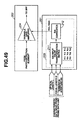
- FIG. 20 to Fig. 22 show a major portion of the second embodiment of the present invention.
- a photo-sensor assemblage 85 is used as a probe information detecting means, which is disposed in both the joint members included in the optical probe 9 and observing device 6 respectively, in place of a micro-switch-inclusive probe detecting means employed in the first embodiment.
- the photo-sensor assemblage 85 composed of a plurality of photo-sensors is incorporated in the joint member 6a included in the observing device 6.
- the photo-sensor assemblage 85 includes a light-emitting element plate 87a on which a plurality of light-emitting elements 86a is mounted, and a light-receiving element plate 87b on which a plurality of light-receiving elements 86b is mounted to face the plurality of light-emitting elements 86a.
- a light interceptor 88 is included in the attachment 10 of the optical probe 9.
- the light interceptor 88 is, as shown in Fig. 21 , interposed between the light-emitting element plate 87a and light-receiving element plate 87b.
- the light interceptor 88 has through holes 89 that face in a direction of light emission in which the plurality of light-emitting elements 87a emit light.
- the light receiving elements 86b communicating with the light-emitting elements 86a by way of the through holes 89 can receive light from the light-emitting elements 86a (on state).
- the light-receiving elements 86b not facing the through holes 89 cannot receive light from the light-emitting elements 86a (off state).
- the light-receiving elements 86b and light-emitting elements 86a are interconnected over a cable 90.
- the cable 90 is routed to a detection circuit incorporated in the computer 18.
- the computer 18 detects the situation of the photo-sensor assemblage 85 receiving light, and thus acquires feature information concerning the optical probe 9.
- Fig. 22 shows the electrical circuitry including a pair of light-emitting element 86a and light-receiving element 86b.
- Light emanating from the light-emitting element 86a is intercepted by the light interceptor 88 but does not enter in the light-receiving element 86b, for example, a photo-transistor.
- the photo-transistor becomes nonconducting, and the collector output inverted by an inverter 91 is driven to an off-state (low) level.
- the light interceptor 88 has the through hole 89 opposed to the pair of light-emitting element 86a and light-receiving element 96b, light emanating from the light-emitting element 86a passes through the through hole 89 and enters in the light-receiving element 86b. In this case, the output inverted by the inverter 91 is driven to an on-state (high) level.
- the arrangement pattern of the through holes 89 in the light interceptor 88 is corresponding to a type of the optical probe 9.
- a square of the number of photo-sensors included in the photo-sensor assemblage 85 corresponds to the number of detectable types of the optical probes 9. For example, as shown in Fig. 21 , if the number of photo-sensors is four, the number of detectable types of probes is 16.
- the present embodiment adopts a method of intercepting light that emanates from the light-emitting elements 86a. Alternatively, a method of reflecting the light may be adopted.
- the present embodiment provides the advantages described below.
- a more inexpensive and compact optical imaging system can be realized due to adoption of a photo-sensor.
- a plurality of photo-sensors juxtaposed in the axial direction can be disposed at one position on the circumference. This contributes to simplification of the system configuration.
- Fig. 23 and Fig. 24 show a major portion of a third embodiment of the present invention.
- a memory module 93 is adopted as a probe information detecting means that links both the joint members included in the optical probe 9 and observing device 6 respectively.
- the memory module 93 is incorporated inside the attachment 10 of the optical probe 9, and connected to a cable connector 95 disposed in the joint member 6a of the observing device 6 through memory connector members 94a connected to the memory module 93.
- the memory connector members 94a have pins thereof coupled to a power line or signal lines, and are connected to the computer 18 over a cable 96 that is coupled to pin receptacles included in the cable connector 95.
- Power required by the memory module 93 is supplied from the computer 18 over the power line. Probe information recorded in advance in the memory module 93 is in turn read into the computer 18 over the signal lines.
- Fig. 24 shows the relationship among the connections. Referring to Fig. 24 , memory cells 94b are sealed inside the memory module 93.
- a matrix (or array) of electronic elements such as resistors may be substituted for the memory module 93.
- a power line and signal lines needed to connect the matrix of electric elements (to detect the electric characteristics thereof) are passed through the joint connector and routed to the computer 18.
- the values indicating the electric characteristics of the electronic elements constituting the matrix are detected as probe feature information. For example, when the electronic elements are resistors, the resistances of the resistors themselves are detected as probe information by the computer 18.
- a larger amount of data or information can be recorded or detected.
- a fourth embodiment of the present invention employs a direct-vision optical probe so as to produce a two-dimensionally observed image (image produced by optical imaging).
- Fig. 25 to Fig. 43 are concerned with the fourth embodiment of the present invention.
- Fig. 25 schematically shows the structure of an optical probe employed in the optical imaging system of the fourth embodiment.
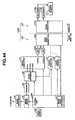
- Fig. 26 is a circuit block diagram schematically showing the configuration of the optical imaging system of the fourth embodiment.
- Fig. 27 is a circuit block diagram schematically showing the configuration of a photo-detector shown in Fig. 26 .
- Fig. 28 includes explanatory diagrams concerning sampling of image data acquired by an optical element and scanned by a scanner.
- Fig. 28(a) is an explanatory diagram concerning X and Y scanning of the optical elements in X and Y directions.
- Fig. 28(b) is a graph indicating a driving frequency at which an X scanner is driven.
- FIG. 28(c) is a graph indicating a driving frequency at which a Y scanner is driven.
- Fig. 28(d) is an explanatory diagram showing sampled image data items that are rearranged in a real space.
- Fig. 29 is an explanatory diagram showing a display image that is composed of dots drawn at regular intervals in order to represent the image data items shown in Fig. 28(d) .
- Fig. 30 includes data tables to be stored in a probe data unit.
- Fig. 30(a) is a data table specifying a type of probe, an optical path length and others.
- Fig. 30(b) is a data table specifying the conditions for driving an X scanner.
- Fig. 30(c) is a data table specifying the conditions for driving a Y scanner.
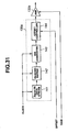
- FIG. 31 is a circuit block diagram schematically showing the configuration of an X drive unit included in a signal generator.
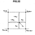
- Fig. 32 is a graph for explaining a bi-linear interpolation.
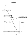
- Fig. 33 and Fig. 34 are graphs concerning the bi-linear interpolation explained in conjunction with Fig. 32 and adapted to the present embodiment.
- Fig. 33 is a graph used to detect the relationship between a data column number Bj and an X-direction interpolation coefficient Kx j .
- Fig. 34 is a graph used to detect the relationship between a data column number Ai and a Y-direction interpolation coefficient Ky j .
- Fig. 35 includes explanatory diagrams concerning interpolation of image data.
- Fig. 35 includes explanatory diagrams concerning interpolation of image data.
- Fig. 35(a) is an explanatory diagram showing sampled image data items rearranged in the real space.
- Fig. 35(b) is an explanatory diagram concerning an interpolation extraction, performed in an odd frame using the bi-linear interpolation method in the state shown in Fig. 35(a).
- Fig. 35(c) is an explanatory diagram concerning aliasing of data, performed in an even frame, in the state shown in Fig. 35(b) .
- Fig. 36 to Fig. 42 are timing charts each including graphs that indicate the timings of signals produced by a signal generator.
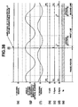
- Fig. 36 is a timing chart including graphs that indicate the timings of signals produced by the signal generator in a steady state.
- Fig. 36 is a timing chart including graphs that indicate the timings of signals produced by the signal generator in a steady state.
- FIG. 36(a) is a graph showing the waveform of a Y driving signal that is a driving signal with which a Y scanner is driven.
- Fig. 36(b) is a graph showing the waveform of a Y-U/D signal with which it is discriminated whether the Y scanner driven with the Y driving signal shown in Fig. 36(a) is on the outward sweep or homeward sweep.
- Fig. 36(c) is a graph showing the waveform of a Y triggering signal (Y-Sync).
- Fig. 36(d) is a graph showing the waveform of an X triggering signal (X-Sync).
- Fig. 36(e) is a graph showing the waveform of a signal having a clock frequency fs.
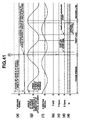
- Fig. 37 is a timing chart including graphs that indicate the timings of signals produced when the Y driving signal assumes a maximum positive value.
- Fig. 37(a) is a graph showing the waveform of the Y driving signal that is a driving signal with which the Y scanner is driven.
- Fig. 37(b) is a graph showing the waveform of the (Y-U/D) signal with which it is discriminated whether the Y scanner driven with the Y driving signal shown in Fig. 37(a) is on the outward sweep or homeward sweep.
- Fig. 37(c) is a graph showing the waveform of the Y triggering signal (Y-Sync).
- Fig. 37(d) is a graph showing the waveform of the X triggering signal (X-Sync).
- Fig. 37(a) is a graph showing the waveform of the Y driving signal that is a driving signal with which the Y scanner is driven.
- Fig. 37(b) is a graph showing the waveform of the (Y
- Fig. 37(e) is a graph showing the waveform of a signal having the clock frequency fs.
- Fig. 37(f) is a graph showing the waveform of an X driving signal that is a driving signal with which the X scanner is driven.
- Fig. 37(g) is a graph showing an angle by which an optical element whose input is scanned by the X scanner is driven in an X direction.
- Fig. 38 is a timing chart including graphs that indicate the timings of signals produced when the Y triggering signal (Y-Sync) is produced in order to initiate a (homeward) sweep for producing the first frame.
- Fig. 38(a) is a graph indicating the waveform of the Y driving signal that is a driving signal with which the Y scanner is driven.
- Fig. 38(b) is a graph indicating the waveform of the (Y-U/D) signal with which it is discriminated whether the Y scanner driven with the Y driving signal shown in Fig. 38(a) is on the outward sweep or homeward sweep.
- Fig. 38(c) is a graph indicating the waveform of the Y triggering signal (Y-Sync).
- Fig. 38(d) is a graph indicating the waveform of the X triggering signal (X-Sync).
- Fig. 38(e) is a graph indicating the waveform of a signal having the clock frequency fs.
- Fig. 38(f) is a graph indicating the waveform of the X driving signal that is a driving signal with which the X scanner is driven.
- Fig. 38(c) is a graph indicating the waveform of the Y triggering signal with which it is discriminated whether the Y scanner driven with the Y driving signal shown in Fig. 38(a) is on the outward sweep or homeward
- Fig. 39 is a timing chart including graphs that indicate the timings of signals produced immediately before sampling of data representing one frame is completed.
- Fig. 39(a) is a graph indicating the waveform of the Y driving signal that is a driving signal with which the Y scanner is driven.
- Fig. 39(b) is a graph indicating the waveform of the (Y-U/D) signal with which it is discriminated whether the Y scanner driven with the Y driving signal shown in Fig. 39(a) is on the outward sweep or homeward sweep.
- Fig. 39 is a timing chart including graphs that indicate the timings of signals produced immediately before sampling of data representing one frame is completed.
- Fig. 39(a) is a graph indicating the waveform of the Y driving signal that is a driving signal with which the Y scanner is driven.
- Fig. 39(b) is a graph indicating the waveform of the (Y-U/D) signal with which it is discriminated whether the Y scanner driven with the Y driving signal
- Fig. 39(c) is a graph indicating the waveform of the Y triggering signal (Y-Sync).
- Fig. 39(d) is a graph indicating the waveform of the X triggering signal (X-Sync).
- Fig. 39(e) is a graph indicating the waveform of a signal having the clock frequency fs.
- Fig. 39(f) is a graph indicating the waveform of the X driving signal that is a driving signal with which the X scanner is driven.
- Fig. 39(g) is a graph indicating an angle by which the optical element whose input is scanned by the X scanner is driven in the X direction.
- Fig. 40 is a timing chart including graphs that indicate the timings of signals produced when the Y driving signal assumes a maximum negative value.
- Fig. 40(a) is a graph indicating the waveform of the Y driving signal that is a driving signal with which the Y scanner is driven.
- Fig. 40(b) is a graph indicating the waveform of the (Y-U/D) signal with which it is discriminated whether the Y scanner driven with the Y driving signal shown in Fig. 40(a) is on the outward sweep or homeward sweep.
- Fig. 40(c) is a graph indicating the waveform of the Y triggering signal (Y-Sync).
- Fig. 40(d) is a graph indicating the waveform of the X triggering signal (X-Sync).
- Fig. 40(e) is a graph indicating the waveform of a signal having the clock frequency fs.
- Fig. 40(b) is a graph indicating the waveform of the (Y-U/D) signal with which it is discriminated whether the Y scanner driven with the Y driving signal shown in Fig. 40(a) is on the outward sweep
- FIG. 40(f) is a graph indicating the waveform of the X driving signal that is a driving signal with which the X scanner is driven.
- Fig. 40(g) is a graph indicating an angle by which the optical element whose input is scanned by the X scanner is driven in the X direction.
- Fig. 41 is a timing chart including graphs that indicate the timings of signals produced when the Y triggering signal (Y-Sync) is produced in order to initiate a (homeward) sweep for producing the second frame.
- Fig. 41(a) is a graph indicating the waveform of the Y driving signal that is a driving signal with which the Y scanner is driven.
- FIG. 41(b) is a graph indicating the waveform of the (Y-U/D) signal with which it is discriminated whether the Y scanner driven with the Y driving signal shown in Fig. 41(a) is on the outward sweep or homeward sweep.
- Fig. 41(c) is a graph indicating the waveform of the Y triggering signal (Y-Sync).
- Fig. 41(d) is a graph indicating the X triggering signal (X-Sync).
- Fig. 41(e) is a graph indicating the waveform of a signal having the clock frequency fs.
- Fig. 41(f) is a graph indicating the waveform of the X driving signal that is a driving signal with which the X scanner is driven.
- Fig. 41(c) is a graph indicating the waveform of the Y triggering signal with which it is discriminated whether the Y scanner driven with the Y driving signal shown in Fig. 41(a) is on the outward sweep or homeward sweep.
- Fig. 41(g) is a graph indicating an angle by which the optical element whose input is scanned by the X scanner is driven in the X direction.
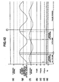
- Fig. 42 is a timing chart including graphs that indicate the timings of signals produced immediately before sampling data that represents the second frame is completed.
- Fig. 42(a) is a graph indicating the waveform of the Y driving signal that is a driving signal with which the Y scanner is driven.
- Fig. 42(b) is a graph indicating the waveform of the (Y-U/D) signal with which it is discriminated whether the Y scanner driven with the Y driving signal shown in Fig. 42(a) is on the outward sweep or homeward sweep.
- Fig. 42 is a timing chart including graphs that indicate the timings of signals produced immediately before sampling data that represents the second frame is completed.
- Fig. 42(a) is a graph indicating the waveform of the Y driving signal that is a driving signal with which the Y scanner is driven.
- Fig. 42(c) is a graph indicating the waveform of the Y triggering signal (Y-Sync).
- Fig. 42(d) is a graph indicating the waveform of the X triggering signal (X-Sync).
- Fig. 42(e) is a graph indicating the waveform of a signal having the clock frequency fs.
- Fig. 42(f) is a graph indicating the waveform of the X driving signal that is a driving signal with which the X scanner is driven.
- Fig. 42(g) is a graph indicating an angle by which the optical element whose input is scanned by the X scanner is driven in the X direction.
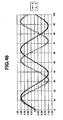
- Fig. 43 is a graph indicating the waveform of a driving signal having a distortion.
- the conventional optical imaging systems have not taken measures to correct an individual difference of an optical probe that is freely detachably attached to a device main body.
- the settings of an optical imaging system dependent on the characteristics of an optical probe can be determined easily.
- the characteristics of an optical probe are detected, and designating means is used to designate the conditions for operation on the basis of the detected information.
- the conventional optical imaging systems include scanning means realized with a scanner but is not designed to control image producing means in consideration of the characteristics of an optical probe.
- the settings for producing an image that is scaled accurately and is devoid of a distortion can be easily determined, and an image devoid of a distortion can be easily produced.
- An optical imaging system in accordance with the present embodiment includes interpolating means. Consequently, even when data is sampled at irregular intervals, an image scaled accurately and devoid of a distortion can be displayed.
- the settings of the interpolating means can be determined based on the characteristic information concerning an optical probe. Thus, the settings optimal to the optical probe can be determined easily.
- a direct-vision type optical scanning probe (hereinafter abbreviated to an optical probe) 101 employed in an optical imaging system 100 of the present embodiment has a fiber 111 such as a single-mode fiber or a multi-mode filter passed through a sheath 110 thereof.
- the sheath 110 has the distal end thereof joined with a cylindrical hard distal cover 113 by way of a hard base member 112.
- the base member 112 has a first sheet 115a that can deform and is included in a scanner 114.
- the first sheet 115a is disposed so that the back end of a second sheet 115b capable of deforming freely will cross the first sheet 115a at right angles via a relay member 116.
- the second sheet 115b has a holder 118, which includes an optical element 117 serving as a convergent optical system, held at the distal end thereof via a coupling member 119.
- the first sheet 115a has a flat first piezoelectric element mounted on the surface thereof.
- the second sheet 115b has a flat second piezoelectric element 120b mounted on the surface thereof.
- the first piezoelectric element and second piezoelectric element 120b are connected to the main body, which will be described later, over a driving cable 121.
- the first piezoelectric element and second piezoelectric element 120b are driven with application of an ac driving signal under the control of the main body. Consequently, the optical element 117 can be driven in a direction orthogonal to the direction of the piezoelectric element.
- the optical element 117 is driven vertically (in an X direction in the coordinate system shown in Fig. 25 ) together with the holder 118.
- the second piezoelectric element 120b and second sheet 115b constitute an X scanner that will be described later.
- the relay member 116 is driven in a direction perpendicular to the sheet of paper of Fig. 25 .
- the optical element 117 is driven in the direction perpendicular to the sheet of paper (in a Y direction in the coordinate system shown in Fig. 25 ). That is to say, the first piezoelectric element and first sheet 115a constitute a Y scanner that will be described later.
- the scanner 114 composed of the X scanner and Y scanner scans light emitted from the optical element 117 two-dimensionally on the XY plane.
- the optical probe 101 is not limited to the one whose scanner 114 has the structure shown in Fig. 25 .
- Various structures shown in the drawings shown, for example, in Japanese Unexamined Patent Application Publication No. 2001-174744 may be adopted as the structure of the scanner 114.
- the optical probe 101 has an opening formed in the distal end face of the cover 37 and opposed to the optical element 117. The opening is blocked with a protective cover glass 122.
- the direct-vision optical probe 101 is, as shown in Fig. 26 , connected to a main body 130 with a probe connector 101a freely detachably attached to a main body connector 130a formed in the main body 130, whereby the optical imaging system 100 is constructed.
- the optical probe 101 includes the X scanner 114a and Y scanner 114b that constitute the scanner 114.
- the X scanner 114a and Y scanner 114b are driven in order to scan the optical element 117 two-dimensionally on the XY plane.
- the X scanner 114a and Y scanner 114b are connected to a signal generator 131 incorporated in the main body 130 through the probe connector 101a and main body connector 130a.
- Driving signals produced by the signal generator 131 are amplified by amplifiers 132a and 132b, and transmitted for the purpose of driving and control.
- Measurement light beam emanating from a light source 133 included in the main body 130 is propagated to the optical element 117 through the probe connector 101a and main body connector 130a over a fiber such as a single-mode fiber.
- the optical element 117 irradiates the measurement light beam to an object while being scanned two-dimensionally on the XY plane by the scanner 114.
- the optical element 117 picks up light returned from the object.
- the picked up return light is propagated to the main body 130 by reversely tracing the path traced by the measurement light beam.
- a photo-detector 134 incorporated in the main body 130 receives the return light and converts it into an electric signal.
- the photo-detector 134 adjusts a gain to be given to the electric signal or filters the electric signal.
- a photo-detection element 134a realized with a photo-diode (PD) or a photomultiplier tube (PMT) receives return light and converts it into an electric signal.
- the electric signal transmitted from the photo-detection element 134a is I-V (current-to-voltage) converted by an I-V converter 134b, and amplified by an amplifier (AMP) 134c.
- AMP amplifier
- a gain to be given by the amplifier 133c is controlled based on a gain control signal sent from a control unit 135.
- the amplified electric signal has low-frequency components thereof cut off by a low-pass filter (LPF) 134d according to a cutoff frequency adjustment signal sent from the control unit 135, and has thus a noise removed therefrom.
- the resultant signal is transmitted to a frame grabber 136.
- the control unit 135 transmits the control signals to the amplifier 134c and low-pass filter 134d respectively on the basis of data stored in a probe data unit 137.
- the frame grabber 136 is a frame memory board including a frame memory in which sampling of an electric signal received from the photo-detector 134, which are acquired based on a signal generated by the signal generator 131, are stored as image data representing one frame, and an A/D converter that analog-to-digital (A/D) converts image data.
- the frame grabber 136 temporarily stores the analog-to-digital converted image data, frame by frame, in a memory 138 of the next stage. The image data is then outputted to an image engine 139.
- the image engine 139 interpolates the image data to rearrange the data items, and then outputs the resultant data items to an image processor 140 (see Fig. 35 ).
- the image processor 140 performs signal processing including DIB conversion, gain/contrast control, gamma correction, resizing, and displaying/transferring, and outputs the resultant signal to a monitor that is not shown. Eventually, an observed image (image produced by optical imaging) is displayed on the display surface of the monitor.
- the optical element 117 is, as shown in Fig. 28(a) to Fig. 28(c) , X-scanned and Y-scanned in X directions and Y directions by the X scanner 114a and Y scanner 114b respectively. If image data items sampled at regular temporal intervals by the frame grabber 136 are rearranged in the real space, they look like, as shown in Fig. 28(d) , being sampled at unequal spatial intervals.
- image data must be corrected so that a resultant image will not suffer a distortion before an image represented by the image data is displayed.
- image data items are interpolated in order to rearrange them (see Fig. 35 ).
- the optical probe 101 includes the probe data unit 137 in which driving information inherent to the probe is stored.
- the control unit 135 reads the information in the probe data unit 137. Based on the read driving information, the control unit 135 predefines a range of adjustable values or the like within which each setting can be adjusted and which is needed to optimize the optical characteristics of the optical scanner probe 2. Compared with a case where the driving information is not read, the optical characteristics of the optical probe can be optimized quickly.
- the control unit 135 is connected to the light source 133, photo-detector 134, and image engine 139, and controls them according to the information read from the probe data unit 137. Moreover, the control unit 135 is connected to the signal generator 131 that produces signals with which the X scanner 114a, Y scanner 114b, and frame grabber 136 are driven and controlled. The X scanner 114a, Y scanner 114b, frame grabber 136, and image engine 139 are driven and controlled with the signals which are produced by the signal generator 131 under the control of the control unit 135.
- the signal generator 131 produces driving signals of, for example, sine waves with which the X scanner 114a and Y scanner 114b are driven.
- the produced driving signals are transmitted through an X-driving terminal (X-Drive) and a Y-driving terminal (Y-Drive).
- the signal generator 131 produces a clock signal, synchronously, with which image data inputted to the frame grabber 136 is sampled at equal temporal intervals, while being interlocked with the X scanner 114a and Y scanner 114b. Moreover, the signal generator 131 produces an X triggering signal (X-Sync) and a Y triggering signal (Y-Sync) synchronously with the clock signal.
- X-Sync X triggering signal
- Y-Sync Y triggering signal
- the signal generator 131 transmits the produced clock signal through a clock terminal thereof, and transmits the produced triggering signals through an X trigger (X-sync) terminal and Y trigger (Y-sync) terminal thereof respectively.
- X-sync X trigger
- Y-sync Y trigger
- the probe data unit 137 is realized with a nonvolatile memory device such as an EEPROM or a flash memory. Data stored in the probe data unit 137 specifies, for example, parameters listed in Fig. 30 .
- the data stored in the probe data unit 137 specifies a type of probe (serial number), an amount of return light (return ratio), an optical path length, a numerical aperture (NA) offered by the optical element 117 (lens), a focal length, a (optical) resolution, an appropriate wavelength of light emanating from a light source, a noise level (a signal-to-noise ratio offered by the probe), and a diameter of a light spot.
- the data stored in the probe data unit 137 specifies, as shown in Fig. 30(b) and Fig. 30(c) , the conditions for driving the X scanner 114a and Y scanner 114b.
- the conditions for driving the Y scanner 114b are, as listed in Fig. 30(c) , the same as the conditions for driving the X scanner 114a, though the letter X is changed to the letter Y.
- the probe data unit 137 is connected to the control unit 135.
- the foregoing data is then read into the control unit 135 in response to a reading signal sent from the control unit 135.
- the data stored in the probe data unit 137 is concerned with the optical characteristics of a scanning optical system including the optical element 117, photo-detector 134, and light source 133, such as, a diameter of a light spot and a resolution or an appropriate wavelength of light emanating from the light source.
- a spatial resolution offered by the scanning optical system is determined with a (optical) resolution r, a scanning velocity, and a sampling rate.
- a constant set in the low-pass filter (LPF) included in the photo-detector 134 of the scanning optical system must be determined to satisfy each set of conditions.
- an amount of return light incident on the photo-detection element 134a varies depending on a difference in assembling of the components of the optical probe 101 or a difference in the design thereof. When unnecessary return light falls on the photo-detection element 134a, it is detected as a noise.
- the optical probe 101 in the optical probe 101, signal components whose levels are lower than the lowest level of noises that are derived from unnecessary return light will not be picked up to determine a resolution of data. Signal levels to be passed or cut off are determined with a range of signal levels which the A/D converter included in the frame grabber 136 can convert.
- the control unit 135 determines the foregoing settings and controls the photo-detector 134.
- the data stored in the probe data unit 137 is concerned with the conditions for driving the scanners; such as, an X positional phase correction coefficient ( ⁇ X ) and an X driving frequency (V X ).
- ⁇ X X positional phase correction coefficient
- V X X driving frequency
- the X scanner 114a is driven at its resonant frequency so that it will be driven on a stable basis to oscillate with a large amplitude.
- the resonant frequency is determined with the mechanical structure of the scanner and the characteristics of a resonator, and may be varied in the course of assembling.
- the resonant frequency value is specified as the X driving frequency fx in the probe data.
- the field of view in an X scanning direction is specified as the X field of view lx.
- the frame grabber 136 is designed so that the above value will be attained in the center of an angle of imaging view and a space between sampling points in the frame grabber will be the longest at the sampling positions near the center of an image.
- the scanning velocity becomes approximately 0. If the frame grabber 136 samples stored data at this time, the number of sampling points gets too large for a display image range. This makes it necessary to greatly increase the size of the image memory included in the grabber, and is therefore not cost-efficient.
- a range of data to be sampled in the frame grabber 136 is limited to the center of the frame grabber and its surroundings (up to 92.5%). Consequently, an unnecessarily large amount of data will not be acquired but sampling can be achieved efficiently.
- the sampled range is stored as the X image range Px in the probe data unit 137.
- the sampling frequency fs shall be adopted as the clock frequency at which the signal generator 131 operates.
- M ( fs / 2 ⁇ fx ⁇ sin - 1 2 ⁇ ⁇ • Px
- Nxc fs / fx
- the signal generator 131 is constituted so as to produce a waveform, which is designated as a type of X driving waveform, so that the waveform will alternate in response to the clock pulses.
- an Xscan(N) data string 141 is read by the X driving terminal (X-Drive) 130a of the signal generator 131 into a reading buffer 142 in response to each clock pulse. Then, a D/A converter 143 performs a digital-to-analog (D/A) conversion for the read column of data. The resultant data is then outputted. Moreover, an offset controller 144 and an amplifier 132a of the X driving terminal 130a control a gain represented by an X driving voltage Vx and an offset represented by an X offset voltage Vxo respectively. Consequently, a driving voltage is transmitted to the X scanner 114a through the X driving terminal 130a.
- the signal generator 131 provides a produced X triggering signal (X-Sync) at the timing deviated by the duration of a subsequent clock pulse from a reference point of a driving waveform (a point at which the amplitude of the driving waveform becomes maximum).
- X-Sync produced X triggering signal
- the signal generator 131 is constructed so as to provide the X triggering signal at the timing of the X triggering point Ntx.
- the X triggering signal (X-Sync) may be provided by the number of lines on which data is acquired after the production of the Y triggering signal (Y-Sync).
- the settings of the Y scanner 114b are determined basically in the same manner as the settings of the X scanner 114a.
- the control unit 135 performs the aforesaid calculations, that is, solves the aforesaid expressions. Calculated are the number of columns of interpolated data L, the number of rows of interpolated data W, the number of sampling points per line M, the number of sampling lines N, the clock frequency fs, the numbers of clock pulses required per cycle Nxc and Nyc, the waveforms Xscan and Yscan, the X and Y triggering points Ntx and Nty, the start position of the X scanner 114a in an X direction t XO , and the start position of the Y scanner 114b in a Y direction t YO .
- the calculated values are inputted to the signal generator 131 and set therein. Consequently, the components can be driven according to the timings shown in the timing chart to be described below.
- the calculated values are also outputted to the frame grabber 136 and image engine 139 and used for sampling and interpolation.
- Data required by the image engine 139 are the above-mentioned L, M, W, N, t XO , t YO and the formulas of driving waveforms used to drive the X scanner 114a and Y scanner 114b respectively.
- the image engine 139 produces a transformation table on the basis of the foregoing data, and interpolates image data items to rearrange the data items as mentioned previously.
- the image engine 139 interpolates image data items, which represent one frame and are temporarily stored in the memory 138, according to, for example, the nearest neighbor interpolation technique or the like, and thus rearranges the data items. Consequently, the positions of dots constituting an image coincide with the positions of sampling points.
- interpolation is a kind of processing used to deform or enlarge an image by producing new dots among dots constituting a raw image.
- the interpolation technique includes, aside from the nearest neighbor interpolation, the bi-linear interpolation and the cubic convolution interpolation.
- the nearest neighbor interpolation is an interpolation technique of adopting a color value exhibited by a dot located nearest to an interpolation dot as a color value of the interpolation dot.
- the bi-linear interpolation is an interpolation technique of adopting an average of color values, which are exhibited by four dots located around an interpolation point, as a color value of the interpolation dot.
- the cubic convolution interpolation is an interpolation technique of interpolating sixteen dots located around the interpolation dot according to the cubic spline technique and adopting the result of interpolation as a color value of the interpolation dot.
- the bi-linear interpolation is adopted for interpolation.
- both the X scanner 114a and Y scanner 114b are driven with sine waveforms.
- L denotes the number of columns of interpolated data
- W denotes the number of rows of interpolated data
- t XO denotes the positional phase of the x scanner 114a at the start position thereof
- t YO denotes the positional phase of the Y scanner 114b at the start position thereof.
- X 0 denotes the start position in an X direction of the X scanner 114a
- Y 0 denotes the start position in a Y direction of the Y scanner 114b
- ⁇ X ⁇ denotes a positional interval in the x direction between interpolated data items
- ⁇ Y ⁇ denotes a positional interval in the Y direction between interpolated data items.
- t Xv arccos X v
- X u cos Bj - 1 ⁇ ⁇ ⁇ t X + t X ⁇ 0
- X u + 1 cos ( Bj ⁇ ⁇ ⁇ t X + t X ⁇ 0
- Y ⁇ cos Ai - 1 ⁇ ⁇ ⁇ t Y + t Y ⁇ 0
- Y u + 1 cos ( Ai ⁇ ⁇ ⁇ t Y + t Y ⁇ 0
- the interpolation coefficient Ky j for the Y-direction value of the dot v ij that is applied to the value of the dot Kyi Y u + 1 - Y ⁇ / Y u + 1 - Y u ⁇ u Ai, Bj is expressed as follows:
- V ij Ky i ⁇ Kx j ⁇ u Ai , Bj + 1 - Kx j ⁇ u Ai , Bj + 1 ⁇ + 1 - Ky i ⁇ Kx j ⁇ u Ai + 1 , Bj + 1 - Kx j ⁇ u Ai + 1 , Bj + 1 where i denotes 1, 2, etc., or L and j denotes 1, 2, etc., or W.
- the image engine 139 interpolates image data items according to the bi-linear interpolation.
- the image engine 139 thus rearranges the image data items, which are sampled at unequal spatial intervals as shown in Fig. 35(a) , in the form shown in Fig. 35(b) or Fig. 35(c) . Thereafter, the image engine 139 performs STC processing such as attenuation correction.
- the direct-vision optical probe 101 is freely detachably attached to the main body 130 and can be replaced with another.
- the optical imaging system 100 irradiates measurement light beam, which emanates from the light source, to an object, and constructs an observed image, which renders the inside of the object, from the information of return light.
- the optical imaging system 100 has the probe data unit 137, which is included in the optical probe 101, connected to the control unit 135. Data in the probe data unit 137 is read into the control unit 135.
- the control unit 135 performs necessary calculations on the read data, and drives and controls the components of the optical imaging system. Thus, the control unit 135 extends control depending on the connected optical probe 101.
- the signal generator 131 produces signals according to the timings shown in any of Fig. 36 to Fig. 42 under the control of the control unit 135.
- the X scanner 114a and Y scanner 114b included in the optical probe 101 are controlled and driven.
- Fig. 36 is a timing chart indicating the timings of signals produced by the signal generator 131 in a steady state.
- Fig. 36(a) is a graph showing the waveform of a Y driving signal that is a driving signal with which the Y scanner 114b is driven.
- the Y driving signal is generated based on the aforesaid waveform data Yscan(N). With output of the Y driving signal, the Y scanner 114b is driven with a sine waveform.
- one cycle of the Y driving signal corresponds to the sum of the durations of Nyc clock pulses.
- Fig. 36(b) is a graph showing the waveform of an on/off (Y-U/D) signal.
- the on/off (Y-U/D) signal assumes an on (Up)-state level to indicate that the Y scanner 114b driven with the Y driving signal shown in Fig. 36(a) scans data representing an odd frame or assumes an off (Down)-state level to indicate that the Y scanner 114b scans data representing an even frame.
- the Y-U/D signal is driven to the on-state level (driven high) when the Y scanner 114b scans data representing an odd frame, subjected to aliasing, and then driven to the off-state level (driven low) when the Y scanner 114b scans data representing an even frame.
- the X scanner 114a is, as shown in Fig. 36(c) to Fig. 36(e) , driven with a sine waveform whose cycle corresponds to a time interval A to F indicated in Fig. 36 .
- Image data acquired by driving the X scanner 114a and Y scanner 114b is sampled synchronously with the driving signals, which are used to drive the scanners, within the frame grabber 136.
- the Y triggering signal (Y-Sync) and X triggering signal (X-Sync) that initiate the sampling, and a signal having the clock frequency fs are outputted according to the timings shown in Fig. 36(c) to Fig. 36(e) .
- the Y triggering signal (Y-Sync) shown in Fig. 36(c) is outputted at the timing deviated by the duration of the next clock pulse Nty from the timing of the Y driving signal assuming the highest level.
- the X triggering signal (X-Sync) shown in Fig. 36(d) is outputted at the timing deviated by the duration of the next clock pulse Ntx from the timing of the X driving signal assuming the highest level.
- Data representing one frame is sampled during a period from outputting of the Y triggering signal (Y-Sync) to the next outputting such that the number of sampling lines will be N.
- n ⁇ denotes 0, ⁇ 1, ⁇ 2, etc.
- the signal having the clock frequency fs need not be synchronized with the X driving positional phase of ⁇ /2+n ⁇ (n denotes 0, ⁇ 1, ⁇ 2, etc.).
- Fig. 37 is a timing chart indicating the timings of signals outputted when the Y driving signal assumes the maximum positive level.
- Fig. 38 is a timing chart indicating the timings of the signals outputted when the Y triggering signal (Y-Sync) is outputted in order to initiate scanning of data representing a first frame (an outward sweep).
- Fig. 39 is a timing chart indicating the timings of the signals outputted immediately before sampling of data representing one frame is completed.
- Fig. 40 is a timing chart indicating the timings of the signals outputted when the Y driving signal assumes the maximum negative level.
- Fig. 37 is a timing chart indicating the timings of signals outputted when the Y driving signal assumes the maximum positive level.
- Fig. 38 is a timing chart indicating the timings of the signals outputted when the Y triggering signal (Y-Sync) is outputted in order to initiate scanning of data representing a first frame (an outward sweep).
- Fig. 39 is a timing chart indicating the timings
- Y-Sync Y triggering signal
- Fig. 37(a) to Fig. 42(a) show the waveforms of the Y driving signal.
- Fig. 37(b) to Fig. 42(b) show the waveforms of the Y-U/D signal.
- Fig. 37(c) to Fig. 42(c) show the waveforms of the Y triggering signal (Y-Sync).
- Fig. 37(d) to Fig. 42(d) show the waveforms of the X triggering signal (X-Sync).
- Fig. 37(e) to Fig. 42(e) show the waveforms of the signal having the clock frequency fs.
- Fig. 37(f) to Fig. 42(f) are graphs showing the waveforms of the X driving signal that is a driving signal used to drive the X scanner 114a.
- the X driving signal is generated based on the aforesaid waveform data Xscan(N). With generation of the X driving signal, the X scanner 114a is driven with a sine waveform. One cycle of the X driving signal corresponds to the sum of the durations of Nxc clock pulses.
- Fig. 37(g) to Fig. 42(g) are graphs showing angles at which the optical element 117 scanned by the X scanner 114a is driven in an X direction.
- the Y-U/D signal is driven to the on-state level.
- the Y-U/D signal is driven to the on-state level, and Nty clock pulses are transmitted. Thereafter, the Y driving signal assumes a level causing the amplitude with which the Y scanner 114b oscillates to fall within the observable range, the Y triggering signal (Y-Sync) is outputted. Synchronously with the Y triggering signal (Y-Sync), Ntx clock pulses are transmitted and the X triggering signal (X-Sync) is then outputted.
- the signal generator 131 outputs a signal to the frame grabber 136 so that data on the first to N-th lines representing the first (1) frame will be sampled within an effective data domain, which is defined with the sampling rate of M sampling points per line, until the Y driving signal approaches to the maximum negative level and the amplitude with which the Y scanner 114b oscillates falls outside the observable range.
- the X triggering signal (X-Sync) is not outputted any more. The pause period starts.
- the Y driving signal assumes a level causing the amplitude of the Y scanner 114b to fall within the observable range. Consequently, the Y triggering signal (Y-Sync) is outputted.
- the X triggering signal (X-Sync) is outputted synchronously with the Y triggering signal (Y-Sync). Outputting of the X triggering signal (X-Sync) does not lag behind outputting of the Y triggering signal (Y-Sync) by the sum of the durations of Ntx clock pulses but lags behind the outputting by a half-waveform length.
- the foregoing control sequence can nullify the difference between the sampling points regarding an odd frame and the sampling points regarding an even frame.
- the signal generator 131 transmits a signal to the frame grabber 136 so that data on the first to N-th line representing the second frame (2) will be sampled within the effective data domain, which is defined with the sampling rate of M sampling points per line, until the Y driving signal approaches to the maximum positive level and the amplitude of the Y scanner 114b falls outside the observable range.
- the X triggering signal (X-Sync) is not outputted any more.
- the pause period starts. Thereafter, the aforesaid actions are repeated.
- image data picked up by the optical element 114 is sampled and arranged as shown with dots in Fig. 35(a) .
- the image engine 139 interpolates the image data as mentioned above in conjunction with Fig. 35(a) to Fig. 35(c) , and then outputs the resultant data to the image processor 140.
- the image processor 140 performs signal processing such as display and transfer, and outputs the resultant signal to the monitor. Consequently, an observed image (image produced by optical imaging) is displayed on the display surface of the monitor.
- the optical imaging system 100 of the present embodiment can produce an ideal image devoid of a distortion. Moreover, the optical imaging system 100 of the present embodiment can operate on a stable basis because actions are all performed synchronously.
- the optical imaging system 100 of the present embodiment has been described on the assumption that a display scanner is included for scanning the optical element 117 in X and Y directions.
- a three-dimensional display scanner that includes, in addition to the X and Y scanners, a Z scanner for scanning the optical element in Z directions (optical-axis directions) may be adopted. It goes without saying that the present embodiment can implement the three-dimensional scanner in the same manner with the two-dimensional scanner.
- the conditions for scanning and sampling may be calculated based on the L value (number of columns of interpolated data items) and the W value (number of rows of interpolated data items).
- the clock frequency fs may be set to a value closest to the value calculated according to the expression (1), and the subsequent calculations may be carried out.
- an optical imaging system may have the Nxc and Nyc values predetermined.
- the clock frequency fs may then be determined based on the relationship thereof to the Nxc value.
- the signal generator 131 in the optical imaging system can be simplified.
- the X scanner 114a and Y scanner 114b are driven with a distinct sine waveform.
- the scanners may be, as shown in Fig. 43 , driven at a driving frequency at which the scanners do not oscillate ideally and image signals scanned by the scanners contain a distortion.
- the scanning characteristics of the scanners are recorded in the form of approximate expressions in the probe data unit 137.
- the approximate expressions are fifth-order approximate expressions.
- X a 1 ⁇ t 5 + a 2 ⁇ t 4 + a 3 ⁇ t 3 + a 4 ⁇ t 1 + a 5 ⁇ t 6
- Y b 1 ⁇ t 5 + b 2 ⁇ t 4 + b 3 ⁇ t 3 + b 4 ⁇ t 1 + b 5 ⁇ t 6
- X denotes the direction of a field of view
- t denotes a positional phase attained within a scanning cycle
- a 1 to a 6 denote approximation coefficients.
- the interpolation expressions are replaced with the approximate expressions. This enables calculation of the interpolation coefficients.
- the X scanner 114a is driven with a sine waveform and scans data by performing a one-way sweep.
- the X scanner 114a may scan data by performing two sweeps of outward and homeward during one cycle of the sine waveform.
- the optical imaging system 100 should merely generate two X triggering signals (X-Sync) (that are out of positional phase with each other by ⁇ ) during one cycle of an X driving signal.
- X-Sync X triggering signals
- control unit 135 solves a determinant presented below, and the frame grabber 136 rearranges in advance even rows of data to be scanned.
- the resultant data is then outputted to the image engine 139.
- N 21 ⁇ ⁇ N 22 ⁇ ⁇ N 23 ⁇ ⁇ ⁇ ⁇ ⁇ N 2 ⁇ M ⁇ ⁇ 0 , 0 , 0 , . . . . , 0 , 1 0 , 0 , 0 , . . . . 0 , 1 , 0 0 , 0 , 0 , 0 , 0 , . . . . .
- M denotes the number of sampling points per line.
- the time during which sampling can be made longer than the time during which data is scanned. This results in fast scanning.
- Fig. 44 and Fig. 45 are concerned with a fifth embodiment of the present invention.
- Fig. 44 is a circuit block diagram schematically showing the configuration of an optical imaging system in accordance with the fifth embodiment.
- Fig. 45 is a circuit block diagram showing a variant of the optical imaging system shown in Fig. 44 .
- the optical probe 101 includes the probe data unit in which inherent data is held.
- data concerning probes employed is held in the control unit 135.
- the other characteristics are identical to those of the fourth embodiment, and the description thereof will therefore be omitted.
- the components identical to those of the fourth embodiment will be described with the same reference numerals assigned thereto.
- an optical imaging system 100B of the fifth embodiment has a probe data database 151, which is constituted of a nonvolatile memory such as a hard disk drive (HDD), included in a control unit 135b.
- the probe data database 151 receives data concerning optical probes employed and saves it.
- an input device 152 such as a keyboard is used to enter a numerical value
- the data concerning the optical probe 101 is saved.
- data may be copied from any other storage means such as a floppy disk (registered trademark) into the probe data database 151.
- an operator handles the input device 152 based on the attached optical probe 101.
- data of a desired probe is read from the probe data database 151.
- the control unit 135 then outputs set values to the image engine 139, signal generator 131, and frame grabber 136 in the same manner as it is in the fourth embodiment, and thus establishes an observable state.
- the operator operates the optical imaging system 100B to start scanning and observation.
- the optical imaging system 100B operates to produce an image devoid of a distortion.
- optical imaging system 100B of the fifth embodiment even when the optical probe 101 includes no memory, optimal conditions for driving can be easily designated.
- the optical imaging system may have the configuration shown in Fig. 45 .
- an optical imaging system 100C has a memory 153, in which a type of probe and a serial number thereof are recorded, included in an optical probe 101C.
- the control unit 135 reads the type of probe and serial number thereof from the memory 153 included in the optical probe 101. Thereafter, the control unit 135 selects setting information concerning the probe from the probe data database 151, and calculates set values to be set in the image engine 139, frame grabber 136, signal generator 131, and photo-detector 134. The calculated set values are outputted, and the conditions for operation are designated. Thereafter, the operator operates the optical imaging system 100C to start scanning and observation.
- the memory included in the optical probe is small in size. Nevertheless, automatic designation is achieved. This leads to improved maneuverability.
- Fig. 46 to Fig. 48 are concerned with a sixth embodiment of the present invention.
- Fig. 46 is a graph showing the waveforms of driving signals used to drive the X scanner and Y scanner at nearly identical resonant frequencies.
- Fig. 47 is a graph showing a pattern of scanning spots explored by the X scanner and Y scanner that are driven with the driving signals shown in Fig. 46 .
- Fig. 48 is a graph showing sampling points attained by continuing scanning as the one shown in Fig. 47 .
- Conventional optical imaging systems include the one disclosed in, for example, Japanese Unexamined Patent Application Publication No. 2000-75210 and designed to use two scanners to scan Lissajous figures.
- the proposed optical imaging system has not been described about the conditions for driving scanners, the details of an operating procedure, and imaging.
- the present embodiment attempts to lower driving voltages by driving a plurality of scanners at resonant frequencies. Moreover, a field of view for observation is widened.
- the conditions for driving are designated based on characteristic information of an optical probe. Consequently, driving positional phases at which the scanners are driven can be accurately matched, and scanning can be achieved without a deviation.
- the X scanner 114a and Y scanner 114b are driven at nearly identical resonant frequencies.
- the other characteristics are identical to those of the fourth embodiment, and the description thereof will therefore be omitted. Identical components will be described with the same reference numerals assigned thereto.
- the driving frequency fy at which the Y scanner 114b is driven is set to a value close to but a bit different from the driving frequency fx at which the X scanner 114a is driven.
- the X scanner 114a is driven at the driving frequency of 10 kHz
- the Y scanner 114b is driven at the driving frequency of 11 kHz.
- the scanners make a wavy movement with every attainment of a frequency of 1 kHz.
- the scanners scan data to draw a scanning pattern like the one shown in Fig. 47 because of the wavy movements.
- image data is acquired from sampling points shown in Fig. 48 .
- the relationship between the scanning and sampling points is identical to the one described in relation to the fourth embodiment.
- the control unit 135 sets the driving frequency fy of the Y scanner 114b, which is close to but a bit different from the driving frequency fx of the X scanner 114a, to a value fy0.
- the control unit 135 then references positional phase difference information concerning the Y scanner 114b, determines the positional phase of the driving waveform, and sets the frame rate to fx-fy.
- the number of sampling points per cycle is calculated as (fx-fy)/fs.
- Data items present in a range defined with an X image range Px and a Y image range Py should be acquired. Based on the data items present in the range defined with the X image range P and Y image range Py, the control unit 135 outputs a triggering signal, with which image data is acquired, to the frame grabber 136. The data is sampled only for the portion where a clock pulse is enabled.
- the frame grabber 136 temporarily stores frame by frame the sampled time-sequential image data in the memory 138 on the next stage, and then outputs the data to the image engine 139.
- the image engine 139 uses a transformation table to transform the image data read from the memory 138 into spatially mapped data from the time-sequential data.
- the image data transformed using the table is interpolated by the image engine 139 in the same manner as it is in the fourth embodiment, and processed for display by an image processor 140.
- the resultant data is outputted to a monitor that is not shown.
- the optical imaging system of the sixth embodiment drives the Y scanner 114b at a resonant frequency close to the resonant frequency of the X scanner 114a. Therefore, the Y scanner also can acquire a high scanning amplitude in response to a low driving voltage. This means that the system can be driven with a low voltage. This results in a high frame rate and permits scanning over a wide range.
- Fig. 49 to Fig. 61 are concerned with a seventh embodiment of the present invention.
- Fig. 49 is a circuit block diagram schematically showing a major portion of an optical imaging system in accordance with the seventh embodiment.
- Fig. 50 includes graphs showing characteristic curves that are inputted to a D/A input value transformation matrix shown in Fig. 49 .
- Fig. 50(a) is a graph showing a characteristic curve indicating an amount of return light with respect to an optical path length L.
- Fig. 50(b) is a graph showing a characteristic curve indicating an amount of return light with respect to a focal length D.
- Fig. 50(c) is a graph showing a characteristic curve indicating an amount of return light versus a numerical aperture NA.
- Fig. 50 is a circuit block diagram schematically showing a major portion of an optical imaging system in accordance with the seventh embodiment.
- Fig. 50 includes graphs showing characteristic curves that are inputted to a D/A input value transformation matrix shown in Fig.
- Fig. 51 is a flowchart describing gain control.
- Fig. 52 is a circuit block diagram showing a variant of the optical imaging system shown in Fig. 49 .
- Fig. 53 includes explanatory diagrams concerning a calculation mode of calculating a gain control level.
- Fig. 53(a) is an explanatory diagram concerning a calculation mode of calculating a gain control level to be applied to data representing the whole of a specific frame.
- Fig. 53(b) is an explanatory diagram concerning a calculation mode of calculating a gain control level to be applied to data representing all of a plurality of successive frames.
- Fig. 53(a) is an explanatory diagram concerning a calculation mode of calculating a gain control level to be applied to data representing all of a plurality of successive frames.
- FIG. 53(c) is an explanatory diagram showing a calculation mode of calculating a gain control level to be applied to data representing the whole area of each frame of a plurality of frames that is chosen by every specific number of frames.
- Fig. 53(d) is an explanatory diagram concerning a calculation mode of calculating a gain control level to be applied to data representing a specific area in a specific frame.
- Fig. 53(e) is an explanatory diagram concerning a calculation mode of calculating a gain control level to be applied to data representing the specific areas in a plurality of successive frames.
- FIG. 53(f) is an explanatory diagram concerning a calculation mode of calculating a gain control level to be applied to data representing the specific areas in every frame of a plurality of frames that is chosen by every specific number of frames.
- Fig. 54 is a flowchart describing gain control.
- Fig. 55 is a flowchart describing gain calculation.
- Fig. 56 is a flowchart describing processing "a" mentioned in Fig. 55 .
- Fig. 57 is a flowchart describing processing "b” mentioned in Fig. 55 .
- Fig. 58 is a flowchart describing processing "c” mentioned in Fig. 55 .
- Fig. 59 is a flowchart describing processing "d” mentioned in Fig. 55 .
- Fig. 60 is a flowchart describing processing "e” mentioned in Fig. 55 .
- Fig. 61 is a flowchart describing processing "f” mentioned in Fig. 55 .
- the properties of return light coming from an object of observation are measured in advance, and a gain is controlled based on the properties.
- the properties of return light must be measured for each optical probe whose optical characteristics are different from references. Gain control is thus labor-intensive. According to the present embodiment, even if optical probes are switched, a gain can be controlled based on information inherent to each optical probe.
- gain control means is included for controlling the sensitivity of a photo-detector to received light.
- the other characteristics are identical to those of the fourth embodiment and the description of the identical characteristics will be omitted. Components identical to those of the fourth embodiment will be described with the same reference numerals assigned thereto.
- the optical imaging system of the seventh embodiment has a gain controller 203, which controls the sensitivity of a photo-detector 202 to received light, incorporated in a control unit 201.
- the photo-detector 202 photoelectrically converts return light propagated from the optical probe 101 to an electric signal.
- a variable gain amplifier 204 controls a gain to be given to the electric signal.
- a band-pass filter (BPF) that is not shown passes frequency components that falls within a predetermined band, and outputs the resultant signal to the frame grabber 136.
- the gain controller 203 includes a D/A input value transformation matrix 211 and a D/A converter 212.
- the D/A input value transformation matrix 211 transforms characteristic data such as an optical path length L, a focal length D, a numerical aperture NA, or the like that are received from the probe data unit 137, into matrix data.
- the D/A input value transformation matrix 211 multiplies the matrix data by a parameter to work out a gain control level that is a coefficient correction value used for gain control.
- the D/A converter 212 digital-to-analog (D/A) converts the gain control level calculated by the D/A input value transformation matrix 211, and outputs the resultant value as a voltage value to an input stage of the variable gain amplifier 204 included in the photo-detector.
- the characteristic data received by the D/A input value transformation matrix 211 is a numerical value representing an amount of return light relevant to the optical path length L, focal length D, or numerical aperture NA as indicated with any of the graphs of Fig. 50(a) to Fig. 50(c) .
- the graph shown in Fig. 50(a) indicates an amount of return light propagated from the optical probe 101 relative to the optical path length L.
- the graph shown in Fig. 50(b) indicates an amount of return light propagated from the optical probe 101 relative to the focal length D.
- the graph shown in Fig. 50(c) indicates an amount of return light propagated from the optical probe 101 relative to the numerical aperture (NA).
- the probe data unit 137 is connected to the control unit 201.
- the control unit 201 reads data from the probe data unit 137.
- the control unit 201 then controls a gain to be given by the photo-detector as described in the flowchart of Fig. 51 .
- control unit 201 reads characteristic data (specifying the optical path length L, focal length D, or numerical aperture (NA)) from the probe data unit 137 at the D/A input value transformation matrix 211 (step S1).
- the control unit 201 uses the D/A input value transformation matrix 211 to transform the characteristic data into matrix data, multiplies the matrix data by a parameter, and then works out a gain control level (step S2).
- the control unit 201 uses the D/A converter 212 to convert the gain control level into an analog voltage value ranging from, for example, 0 to 2 V (step S3).
- control unit 201 outputs the analog voltage to the variable gain input stage of the variable gain amplifier 204 included in the photo-detector, uses the variable gain amplifier 204 to control a gain (step S4), and then terminates the gain control (step S5).
- a gain to be given by the photo-detector can be controlled. Even when optical probes 101 are changed and the optical characteristics including the optical path length are varied, the sensitivity of the photo-detector to received light can be optimized.
- the D/A converter 212 employed is of a voltage output type.
- a D/A converter 212 of a current output type or an I-V converter may be employed.
- an analog switch may be substituted for the D/A converter 212.
- the analog switch is used to switch resistance values, whereby an input value to the variable gain input stage of the variable gain amplifier 204 is determined.
- a general-purpose amplifier may be substituted for the variable gain amplifier 204 and designed to have a ratio of feedback resistances thereof made variable.
- the optical imaging system may have the components shown in Fig. 52 .
- the optical imaging system includes a D/A input value transformation matrix 211b and a gain controller 203B.
- the D/A input value transformation matrix 211b transforms characteristic data such as an optical path length L, a focal length D, a numerical aperture (NA), or the like that are read from the probe data unit 137, into matrix data.
- the D/A input value transformation matrix 211b then multiplies the matrix data by a parameter, and thus works out a luminance value.
- the gain controller 203B includes a gain calculator 213 that uses the obtained luminance value to work out a gain control level according to a calculation mode dependent on the number of frames or the like, and that outputs the gain control level to the D/A converter 212.
- the calculation mode includes those indicated in Fig. 53(a) to Fig. 53(f) .
- a calculation mode indicated in Fig. 53(a) is a mode of calculating a gain control level to be applied to data representing the whole area of a specific frame.
- a calculation mode indicated in Fig. 53(b) is a mode of calculating a gain control level to be applied to data representing all of a plurality of consecutive frames.
- a calculation mode indicated in Fig. 53(c) is a mode of calculating a gain control level to be applied to data representing the whole area of each frame of a plurality of frames that is chosen by every specific number of frames.
- a calculation mode indicated in Fig. 53(d) is a mode of calculating a gain control level to be applied to data representing a specific area in a specific frame.
- a calculation mode indicated in Fig. 53(e) is a mode of calculating a gain control level to be applied to data representing specific areas in a plurality of consecutive frames.
- a calculation mode indicated in Fig. 53(f) is a mode of calculating a gain control level to be applied to data representing specific areas in each frame of a plurality of frames that is chosen by every specific number of frames.
- the control unit 201 controls a gain to be given by the photo-detector by calculating a gain control level according to a calculation mode indicated in any of Fig. 53(a) to Fig. 53(f) as described in the flowchart of Fig. 54 .
- control unit 201 reads characteristic data (an optical path length L, focal length D, or numerical aperture (NA)) from the probe data unit 137 at the data to the D/A input value transformation matrix 211b (step S1').
- characteristic data an optical path length L, focal length D, or numerical aperture (NA)
- the control unit 201 uses the D/A input value transformation matrix 211b to transform the characteristic data into matrix data, and multiplies the matrix data by a parameter to work out a luminance value (step S2').
- the control unit 201 calculates a gain as described in Fig. 55 (step S10). Thereafter, the control unit 201 uses the D/A converter 212 to convert a gain control level into an analog voltage value ranging from, for example, 0 to 2 V (step S3').
- control unit 201 outputs the analog voltage to the variable gain input stage of the variable gain amplifier 204 included in the photo-detector, and thus controls a gain to be given by the variable gain amplifier 204 (step S4').
- the gain control is then terminated (step S5').
- step S10 gain calculation (step S10) to be performed by the gain calculator 213 will be described using the flowchart of Fig. 55 .
- the gain calculator 213 judges whether gain calculation is performed according to a calculation mode (step S11). If gain calculation is performed, it is judged whichever of the calculation modes is selected (step S12 to S17).
- the gain calculator 213 normalizes a gain control level to a value ranging, for example, on condition 8-bit data is employed, from 0 to 255 (step S18). Gain calculation is then terminated (step S19).
- the gain calculator 213 performs processings "a" to "f" (steps S20 to S70) according to the adopted calculation mode. Control is then returned to step S11.
- steps S20 to S70 are described in the flowcharts of Fig. 56 to Fig. 61 .
- the processing "a" is to detect maximum and minimum luminance values within an object domain that corresponds to data representing the whole area of one specific frame, and calculates a median (step S21).
- the gain calculator 213 transmits the calculated median to the D/A converter 212 (step S22), and terminates the processing a (step S23).
- the gain calculation may result in an average or a value calculated based on a luminance characteristic instead of the median. The same applies to the subsequent flowcharts.
- the gain calculator 213 performs the processing "a”, as the processing "b", on an object domain which corresponds to data representing the whole area of one specific frame (step S20). It is then judged whether the processing should be terminated (step S31). If the processing should not be terminated, calculation object data is changed to data representing the next frame (step S32) and control is then returned to step S20. If the processing should be terminated, the gain calculator 213 terminates the processing "b" (step S33).
- the gain calculator 213 judges as the processing "c" whether an object frame is designated (step S41). If so, the processing "a" is performed on data representing the whole area of the specific frame (step S20). Thereafter, calculation object data is changed to data representing the next frame (step S42) and control is then returned to step S20. If no object frame is specified, the gain calculator 213 terminates the processing "c" (step S43).
- the gain calculator 213 designates as the processing "d” an object domain (x1, y1), (x2, y2) as a specific domain within data representing a specific frame (step S51), and performs the processing "a” on the designated object domain (step S20). The gain calculator 213 then terminates the processing "d” (step S52).
- the gain calculator 213 designates as the processing "e” an object domain (x1, y1), (x2, y2) as a specific domain within data representing one specific frame (step S61), and performs the processing "b” on the specified object domain within the data representing one frame (step S30). The gain calculator 213 then terminates the processing "e” (step S62).
- the gain calculator 213 designates as the processing "f" an object domain (x1, y1), (x2, y2) as a specific domain within data representing a specific frame (step S71), and then performs the processing "c” on the specified object domain within the data representing the specific frame (step S40). The gain calculator 213 then terminates the processing "f” (step S72).
- the optical imaging system of the present variant provides the same advantages as the one of the seventh embodiment.
- gain calculation is performed according to a calculation mode dependent on the number of frames or the like.
- the sensitivity of the photo-detector to received light can be optimized.
- Fig. 62 to Fig. 65 are concerned with an eighth embodiment of the present invention.
- Fig. 62 is a circuit block diagram schematically showing a major portion of an optical imaging system in accordance with the eighth embodiment.
- Fig. 63 is a graph indicating the frequency characteristic of a band-pass filter (BPF) shown in Fig. 62 .
- Fig. 64 is a flowchart describing filter adjustment.
- Fig. 65 is a graph concerning correction of a gamma indicated in an output signal y in relation to that indicated in an input signal x.
- BPF band-pass filter
- the eighth embodiment includes a filter adjusting means that regulates the cutoff frequency of a photo-detector.
- the other characteristics are identical to those of the fourth embodiment, and the description of the identical characteristics is omitted. A description will proceed with the same reference numerals assigned to identical components.
- the present embodiment includes a band adjusting means that even when optical probes are changed, can regulate a frequency band according to information inherent to each optical probe. Thus, the present embodiment can automatically regulate a frequency band of signal components that can pass through an optical probe.
- an optical imaging system of the eighth embodiment has a filter regulator 220, which regulates the cutoff frequency of the photo-detector 202, included in the control unit 201.
- the photo-detection element 117 photoelectrically converts return light propagated from the optical probe 101 into an electric signal.
- the variable gain amplifier 204 described in relation to the seventh embodiment controls a gain to be given to the electric signal.
- the band-pass filter (BPF) 230 passes frequency components, which fall within a predetermined frequency band, and outputs the resultant signal to the frame grabber 136.
- the band-pass filter 230 includes a low-pass filter (LPF) 231 and a high-pass filter (HPF) 232.
- the low-pass filter 231 cuts off the low-frequency components of the electric signal, which is received from the variable gain amplifier 204, according to coefficient data (normalization value) sent from the filter regulator 220.
- the high-pass filter 232 cuts off, like the low-pass filter 231, the high-frequency components of the electric signal, which has the low-frequency components thereof cut off by the low-pass filter 231, according to coefficient data (normalization value) sent from the filter regulator 220.
- the low-pass filter 231 includes a low-frequency D/A converter 233a, an I-V converter 234, and a capacitor C L .
- the low-frequency D/A converter 233a digital-to-analog (D/A) converts the electric signal received from the variable gain amplifier 204, and outputs a current proportional to the coefficient data (normalization value) sent from the filter regulator 220.
- the I-V converter 234 current-to-voltage (I-V) converts the current received from the low-frequency D/A converter 233a.
- the capacitor C L passes only the low-frequency components of the current received from the I-V converter 234.
- the high-pass filter 232 includes a high-frequency D/A converter 233b and a capacitor C H .
- the high-frequency D/A converter 233b digital-to-analog converts the electric signal received from the variable gain amplifier 204, and outputs a current proportional to the coefficient data (normalization value) sent from the filter regulator 220.
- the capacitor C H passes the high-frequency components of the electric signal that has the low-frequency components thereof cut off by the low-pass filter 231.
- the filter regulator 220 includes a filter cutoff frequency arithmetic unit 221, a low-frequency normalization unit 222a, and a high-frequency normalization unit 222b.
- the filter cutoff frequency arithmetic unit 221 calculates a low-pass filter cutoff frequency f L and a high-pass filter cutoff frequency f H from characteristic data specifying a scanner driving frequency f (X driving frequency V X and Y driving frequency V Y ), field of view w (X field of view l X and a Y field of views l Y ), and an optical resolution r.
- the low-frequency normalization unit 222a normalizes the low-pass filter cutoff frequency f L calculated by the filter cutoff frequency arithmetic unit 221, and transmits the resultant value as the coefficient data used to regulate the cutoff frequency of the low-pass filter.
- the high-frequency normalization unit 222b normalizes the high-pass filter cutoff frequency f a calculated by the filter cutoff frequency arithmetic unit 221, and transmits the resultant value as the coefficient data used to regulate the cutoff frequency of the high-pass filter.
- the band-pass filter 230 exhibits the frequency characteristic like the one shown in, for example, Fig. 63 .
- the frequency characteristic is graphically expressed with the Gaussian distribution.
- the center frequency fc and bandwidth ⁇ f are used to calculate the low-pass filter cutoff frequency f L and high-pass filter cutoff frequency f H .
- the coefficients 2 and 0.882 employed in calculation of the center frequency fc and bandwidth ⁇ f can be varied properly.
- the probe data unit 137 is connected to the control unit 201.
- the control unit 201 reads data from the probe data unit 137.
- the control unit 201 then performs filter adjustment (cutoff frequency adjustment) on the photo-detector as described in the flowchart of Fig. 64 .
- the filter cutoff frequency arithmetic unit 221 reads the characteristic data (scanner driving frequency f, field of view w, or optical resolution r) from the probe data unit 137 (step S81). In the control unit 201, the filter cutoff frequency arithmetic unit 221 calculates the center frequency fc of an output of the band-pass filter 230 (step S82).
- the filter cutoff frequency arithmetic unit 221 calculates the bandwidth ⁇ f of the output of the band-pass filter 230 from the center frequency fc (step S83).
- the filter cutoff frequency arithmetic unit 221 calculates the low-pass filter cutoff frequency f L using the center frequency fc and bandwidth ⁇ f (step S84), and also calculates the high-pass filter cutoff frequency f H (step S85).
- control unit 201 normalizes the low-pass filter cutoff frequency f L to a value ranging from, for example, on condition 8-bit data is employed, 0 to 255 so that the low-pass filter cutoff frequency f L will be equal to a cutoff frequency 1/(2 ⁇ R L C L ) determined with the resistance of an internal resistor R L included in the low-frequency D/A converter 233a and the capacitance of the capacitor C L included therein (step S86).
- the high-pass filter cutoff frequency f H is normalized to a value ranging from, for example, on condition 8-bit data is employed, 0 to 255 so that it will be equal to a cutoff frequency 1/(2 ⁇ R H C H ) determined with the resistance of an internal resistor R H included in the high-pass D/A converter 233b and the capacitance of the capacitor C H included therein (step S87).
- control unit 201 inputs the electric signal, which is sent from the variable gain amplifier 204, to the reference voltage input stage of the low-frequency D/A converter 233a included in the low-pass filter 231.
- the control unit 201 then instructs the low-frequency D/A converter 233a to transmit a current proportional to the normalized value of the low-pass filter cutoff frequency f L to the I-V converter 234 (step S88).
- the I-V converter 234 current-to-voltage (I-V) converts the current received from the low-frequency D/A converter 233a.
- the capacitor C L passes the low-frequency components of the current received from the I-V converter 234 and outputs the resultant current to the capacitor C H included in the band-pass filter 230 (step S89).
- the capacitor C H passes only the high-frequency components of the electric signal received from the capacitor C L , and outputs the resultant signal to the frame grabber 136 (step S90). Then, filter adjustment is terminated (step S91).
- the employed D/A converter 212 is of a current output type.
- a voltage output type D/A converter 212 and an analog multiplier may be used to vary a gain to be given by the I-V converter 234.
- the cutoff frequency may be regulated.
- the optical imaging system of the present embodiment may not include the D/A converter 212. Instead, an analog switch is used to switch resistances so as to regulate the cutoff frequency.
- the internal resistor R and capacitor C included in the D/A converter 212 constitute a filter.
- a combination of the internal resistor R and a coil L or a combination of the internal resistor R, coil L, and capacitor C will do.
- the I-V converter 234 may be included or excluded. Anyhow, a known filter will do.
- a predetermined gamma relative to an object of observation is calculated in advance.
- a measured gamma is corrected based on the calculated value. Therefore, in the conventional optical imaging systems, every time optical probes whose optical characteristics are different from references are changed, a gamma must be measured and controlled.
- An image signal producing means is therefore included for correcting a gamma according to information inherent to each optical probe even when optical probes are changed.
- a signal sent from the frame grabber 136 to the image engine 139 via the memory 138 has a gamma component thereof corrected using a function shown in Fig. 65 .
- An image is then displayed on the display surface of a monitor that is not shown.
- the gamma value has the relationship of 0 ⁇ 1.
- a value calculated in advance in order to permit optimal image display based on a signal representing living-body information for example, a value of 0.45 is adopted.
- signal data represents a gray-scale level (ranging from 0 to 255) with eight bits. Alternatively, the data may be able to represent a higher gray-scale level.
- a connected optical probe can be driven or controlled suitably to a scanning technique implemented therein, a light path can be adjusted suitably, or a display image can be adjusted optimally.
Abstract
Claims (29)
- Système d'imagerie optique (1) pour projeter une lumière qui provient d'une source de lumière (2) et construire une image observée d'un objet en fonction d'une information de lumière de retour reçue de l'objet, ledit système d'imagerie optique comprenant :une sonde optique (9) remplaçable pour propager la lumière, qui provient de ladite source de lumière (2), jusqu'à un objet (12), et recevoir une lumière de retour de l'objet (12) ;un corps principal de dispositif incluant un moyen de réception de lumière qui reçoit une lumière de retour de ladite source de lumière (2) et dudit objet (12), et convertit la lumière en un signal électrique, et ayant ladite sonde optique (9) fixée de façon librement détachable à celui-ci ;un moyen de détection pour détecter les caractéristiques d'une sonde optique (9) fixée audit corps principal ;un moyen de désignation pour désigner les conditions de commande d'une sonde optique en fonction des caractéristiques de la sonde optique détectées par ledit moyen de détection ; etledit système d'imagerie optique est caractérisé en ce queau moins l'une d'une plage focale, d'une position focale et d'une ouverture numérique de la sonde optique étant incluse dans les caractéristiques de la sonde optique (9).
- Procédé de détection par imagerie optique pour projeter une lumière qui provient d'une source de lumière (2) et construire une image observée d'un objet (12) en fonction d'une information de lumière de retour reçue de l'objet (12), dans lequel :ledit procédé de détection par imagerie optique est mis en oeuvre dans un système d'imagerie optique (1) comprenant : une sonde optique (9) remplaçable pour propager la lumière, qui provient de ladite source de lumière (2), jusqu'à un objet (12), et recevoir une lumière de retour de l'objet (12) ; un moyen de réception de lumière pour recevoir une lumière de retour de ladite source de lumière (2) et dudit objet (12), et convertir la lumière en un signal électrique ; un corps principal auquel ladite sonde optique (9) peut être fixée de façon librement détachable ; et un moyen de détection pour détecter les caractéristiques d'une sonde optique (9) fixée audit corps principal ;les conditions de commande d'une sonde optique (9) sont désignées sur la base des caractéristiques de la sonde optique (9) détectées par ledit moyen de détection ; etle procédé est caractérisé en ce queau moins l'une d'une plage focale, d'une position focale et d'une ouverture numérique de la sonde optique étant incluse dans les caractéristiques de la sonde optique (9).
- Sonde optique (9) pour propager une lumière, qui provient d'une source de lumière (2), jusqu'à un objet (12), et recevoir une lumière de retour de l'objet (12), comprenant :un moyen de mémoire dans lequel les caractéristiques des sondes (9) sont enregistrées de sorte que les caractéristiques d'une sonde (9) fixée de façon librement détachable à un corps principal de dispositif peuvent être lues ; etladite sonde étant caractérisée en ce queau moins l'une d'une plage focale, d'une position focale et d'une ouverture numérique de la sonde optique étant incluse dans les caractéristiques de la sonde optique (9).
- Système d'imagerie optique (1) selon la revendication 1, comprenant en outre :au moins un moyen de balayage pour balayer une lumière qui provient de ladite source de lumière ;un moyen de génération de signal pour entraîner ledit moyen de balayage et générer un signal de synchronisation ;un moyen de stockage sur lequel des informations caractéristiques de sondes optiques (9) sont enregistrées ;un système optique pour projeter une lumière, qui provient de ladite source de lumière (2), jusqu'à un objet (12), et introduire une lumière de retour reçue de l'objet (12) dans ledit moyen de réception de lumière ;un moyen de mémoire dans lequel un signal électrique envoyé dudit moyen de réception de lumière est stocké ;un moyen de production de signal d'image pour transformer des données stockées dans ledit moyen de mémoire de façon à produire un signal d'image ; etun moyen de commande pour changer au moins un des réglages dudit moyen de production de signal d'image et des réglages dudit moyen de génération de signal en fonction des données lues dans ledit moyen de mémoire.
- Procédé de détection par imagerie optique selon la revendication 2, comprenant :une étape de lecture pour lire des données dans un moyen de stockage ;une étape de calcul pour calculer les conditions de commande de ladite sonde optique en fonction des données lues à ladite étape de lecture ;une étape de désignation pour désigner les conditions de commande calculées à ladite étape de calcul ;une étape de commande et d'entraînement pour commander et entraîner ladite sonde optique en fonction des conditions de commande désignées à ladite étape de désignation ; etune étape de traitement d'affichage pour afficher une image en fonction des données d'image acquises par une sonde optique entraînée à ladite étape de commande et d'entraînement.
- Système d'imagerie optique selon la revendication 4, dans lequel ledit moyen de balayage, ledit moyen de stockage et au moins une partie dudit système optique sont inclus dans ladite sonde optique (9) ; et ladite sonde optique (9) est fixée de façon librement détachable à au moins l'un dudit moyen de production de signal d'image et dudit moyen de génération de signal.
- Système d'imagerie optique selon la revendication 4, dans lequel ledit moyen de production de signal d'image inclut un moyen d'interpolation.
- Système d'imagerie optique selon la revendication 4, dans lequel ledit moyen de commande désigne des données pour ledit moyen de génération de signal en fonction d'informations stockées dans ledit moyen de stockage.
- Système d'imagerie optique selon la revendication 4, dans lequel ledit moyen de balayage est entraîné à une fréquence de résonance mécanique.
- Système d'imagerie optique selon la revendication 4, comprenant en outre un moyen de commande de gain pour commander la sensibilité dudit moyen de réception de lumière à la lumière reçue.
- Système d'imagerie optique selon la revendication 4, comprenant en outre un moyen d'ajustement de filtre pour ajuster la bande de fréquence d'un signal électrique devant être transmis audit moyen de mémoire.
- Système d'imagerie optique selon la revendication 4 ou 6, dans lequel les informations stockées dans ledit moyen de stockage incluent au moins l'une d'une fréquence d'entraînement à laquelle au moins un dispositif de balayage est entraîné, d'une tension d'entraînement, d'une tension de décalage et d'une plage d'imagerie.
- Système d'imagerie optique selon la revendication 6, dans lequel les informations stockées dans ledit moyen de stockage incluent au moins l'un d'un type de sonde et d'un numéro de série de celle-ci.
- Système d'imagerie optique selon la revendication 7, dans lequel ledit moyen de commande désigne des données pour ledit moyen d'interpolation en fonction d'informations stockées dans ledit moyen de stockage.
- Système d'imagerie optique selon la revendication 8, dans lequel les données désignées pour ledit moyen de génération de signal sont l'amplitude d'une forme d'onde d'entraînement avec laquelle ledit moyen de balayage est entraîné.
- Système d'imagerie optique selon la revendication 8, dans lequel les données désignées pour ledit moyen de génération de signal sont la fréquence d'une forme d'onde d'entraînement avec laquelle ledit moyen de balayage est entraîné.
- Système d'imagerie optique selon la revendication 8, dans lequel les données désignées pour ledit moyen de génération de signal sont la forme d'onde d'une forme d'onde d'entraînement avec laquelle ledit moyen de balayage est entraîné.
- Système d'imagerie optique selon la revendication 8, dans lequel ledit moyen de génération de signal inclut un générateur d'horloge, et les données désignées pour ledit moyen de génération de signal sont une fréquence d'horloge à laquelle un signal est généré par ledit générateur d'horloge.
- Système d'imagerie optique selon la revendication 8, dans lequel les données désignées pour ledit moyen de génération de signal sont la synchronisation d'un signal de déclenchement délivré en sortie audit moyen de mémoire.
- Système d'imagerie optique selon la revendication 9, dans lequel deux moyens de balayage ou plus sont inclus, et la fréquence de battement des fréquences auxquelles les deux moyens de balayage ou plus sont entraînés est différente d'un taux de trame.
- Système d'imagerie optique selon la revendication 10, dans lequel ledit moyen de commande désigne des données pour ledit moyen de commande de gain en fonction des informations stockées dans ledit moyen de stockage.
- Système d'imagerie optique selon la revendication 10, dans lequel les données désignées pour ledit moyen de commande de gain sont une quantité de lumière de retour reçue par ledit moyen de réception de lumière.
- Système d'imagerie optique selon la revendication 10, dans lequel ledit moyen de commande de gain inclut un calculateur de gain pour calculer une valeur de correction en fonction de la quantité de lumière de retour.
- Système d'imagerie optique selon la revendication 11, dans lequel ledit moyen de commande désigne des données pour ledit moyen d'ajustement de filtre en fonction des informations stockées dans ledit moyen de stockage.
- Système d'imagerie optique selon la revendication 21, dans lequel ladite quantité de lumière de retour est déterminée avec au moins une longueur de chemin optique pertinent pour ledit système optique, une longueur focale et une ouverture numérique d'un objectif.
- Système d'imagerie optique selon la revendication 23, dans lequel ledit moyen de commande de gain inclut un calculateur de gain qui calcule une valeur de correction en fonction d'une valeur de luminance spécifiée dans des données représentant une zone spécifique dans au moins une trame d'une image.
- Système d'imagerie optique selon la revendication 23, dans lequel ledit moyen de commande de gain calcule une valeur de luminance en utilisant des données représentant chaque trame d'une image, et renvoie la valeur de luminance pour un affichage de la trame suivante.
- Système d'imagerie optique selon la revendication 23, dans lequel ledit moyen de commande de gain calcule une valeur de luminance en utilisant des données représentant au moins une trame spécifique, et renvoie la valeur de luminance pour un affichage des trames suivante et subséquentes.
- Système d'imagerie optique selon la revendication 24, dans lequel les données désignées pour ledit moyen d'ajustement de filtre spécifient une fréquence d'entraînement à laquelle ledit moyen de balayage est entraîné et une résolution offerte par ledit système optique.
Applications Claiming Priority (5)
| Application Number | Priority Date | Filing Date | Title |
|---|---|---|---|
| JP2001139136 | 2001-05-09 | ||
| JP2001139136 | 2001-05-09 | ||
| JP2002115399 | 2002-04-17 | ||
| JP2002115399A JP2003028791A (ja) | 2001-05-09 | 2002-04-17 | 光イメージング装置 |
| PCT/JP2002/004385 WO2002089661A1 (fr) | 2001-05-09 | 2002-05-02 | Dispositif d'imagerie optique et procede de detection d'imagerie optique |
Publications (3)
| Publication Number | Publication Date |
|---|---|
| EP1360927A1 EP1360927A1 (fr) | 2003-11-12 |
| EP1360927A4 EP1360927A4 (fr) | 2008-05-14 |
| EP1360927B1 true EP1360927B1 (fr) | 2010-09-01 |
Family
ID=26614841
Family Applications (1)
| Application Number | Title | Priority Date | Filing Date |
|---|---|---|---|
| EP02769206A Expired - Lifetime EP1360927B1 (fr) | 2001-05-09 | 2002-05-02 | Dispositif d'imagerie optique et procede de detection d'imagerie optique |
Country Status (5)
| Country | Link |
|---|---|
| US (1) | US7072046B2 (fr) |
| EP (1) | EP1360927B1 (fr) |
| JP (1) | JP2003028791A (fr) |
| DE (1) | DE60237505D1 (fr) |
| WO (1) | WO2002089661A1 (fr) |
Cited By (4)
| Publication number | Priority date | Publication date | Assignee | Title |
|---|---|---|---|---|
| US8212884B2 (en) | 2007-05-22 | 2012-07-03 | University Of Washington | Scanning beam device having different image acquisition modes |
| US8305432B2 (en) | 2007-01-10 | 2012-11-06 | University Of Washington | Scanning beam device calibration |
| US8411922B2 (en) | 2007-11-30 | 2013-04-02 | University Of Washington | Reducing noise in images acquired with a scanning beam device |
| US8437587B2 (en) | 2007-07-25 | 2013-05-07 | University Of Washington | Actuating an optical fiber with a piezoelectric actuator and detecting voltages generated by the piezoelectric actuator |
Families Citing this family (50)
| Publication number | Priority date | Publication date | Assignee | Title |
|---|---|---|---|---|
| US7555333B2 (en) | 2000-06-19 | 2009-06-30 | University Of Washington | Integrated optical scanning image acquisition and display |
| US7616986B2 (en) * | 2001-05-07 | 2009-11-10 | University Of Washington | Optical fiber scanner for performing multimodal optical imaging |
| DE10393608B4 (de) * | 2002-10-30 | 2022-06-09 | Optiscan Pty Ltd. | Scanverfahren und - vorrichtung, konfokales Lichtleitfaser-Endoskop, -Mikroskop, oder -Endomikroskop mit einer Scanvorrichtung sowie Lichtleitfaser-Endoskop, -Mikroskop oder - Endomikroskop mit einer Scanvorrichtung |
| JP2004321696A (ja) * | 2003-04-28 | 2004-11-18 | Olympus Corp | 光イメージング装置 |
| US7401984B2 (en) * | 2003-05-16 | 2008-07-22 | Hoya Corporation | Optical connector |
| JP4187160B2 (ja) * | 2003-09-10 | 2008-11-26 | フジノン株式会社 | 断層映像装置 |
| US7901348B2 (en) | 2003-12-12 | 2011-03-08 | University Of Washington | Catheterscope 3D guidance and interface system |
| DE102004008366B3 (de) * | 2004-02-20 | 2005-09-15 | Siemens Ag | Vorrichtung zur Durchführung von Laserangioplastie mit OCT-Überwachung |
| JP4471163B2 (ja) * | 2004-09-30 | 2010-06-02 | 富士フイルム株式会社 | 光断層画像取得装置 |
| US20080107568A1 (en) * | 2004-09-30 | 2008-05-08 | Yoshinori Murashige | Centrifugal Separator and Analyzer with the Same |
| JP5695001B2 (ja) * | 2004-11-02 | 2015-04-01 | ザ ジェネラル ホスピタル コーポレイション | 試料の画像形成のための光ファイバ回転装置、光学システム及び方法 |
| JP2006192059A (ja) * | 2005-01-13 | 2006-07-27 | Fujinon Corp | 断層測定装置 |
| JP2006215006A (ja) * | 2005-02-07 | 2006-08-17 | Fujinon Corp | 光断層画像化装置 |
| JP2006212355A (ja) * | 2005-02-07 | 2006-08-17 | Fujinon Corp | 光断層画像化装置 |
| US7530948B2 (en) | 2005-02-28 | 2009-05-12 | University Of Washington | Tethered capsule endoscope for Barrett's Esophagus screening |
| DE102005021061B4 (de) * | 2005-05-06 | 2011-12-15 | Siemens Ag | Verfahren zur tomographischen Darstellung eines Hohlraumes durch Optische-Kohärenz-Tomographie (OCT) und eine OCT-Vorrichtung zur Durchführung des Verfahrens |
| JP2007101263A (ja) * | 2005-09-30 | 2007-04-19 | Fujifilm Corp | 光断層画像化装置 |
| US8047996B2 (en) * | 2005-10-31 | 2011-11-01 | Volcano Corporation | System and method for reducing angular geometric distortion in an imaging device |
| WO2007067163A1 (fr) | 2005-11-23 | 2007-06-14 | University Of Washington | Faisceau de balayage a cadre sequentiel variable utilisant la resonance de balayage interrompu |
| US20070213618A1 (en) * | 2006-01-17 | 2007-09-13 | University Of Washington | Scanning fiber-optic nonlinear optical imaging and spectroscopy endoscope |
| WO2007084995A2 (fr) * | 2006-01-19 | 2007-07-26 | The General Hospital Corporation | Procedes et systemes pour visualiser de maniere optique des organes intracavitaires epitheliaux lors d'un balayage au faisceau |
| WO2007083376A1 (fr) * | 2006-01-19 | 2007-07-26 | Shofu Inc. | Dispositif de tomographie à cohérence optique et tête de mesure |
| JP2009528128A (ja) | 2006-03-03 | 2009-08-06 | ユニヴァーシティ オブ ワシントン | 多クラッド光ファイバ走査器 |
| US20070216908A1 (en) * | 2006-03-17 | 2007-09-20 | University Of Washington | Clutter rejection filters for optical doppler tomography |
| US20080039693A1 (en) * | 2006-08-14 | 2008-02-14 | University Of Washington | Endoscope tip unit and endoscope with scanning optical fiber |
| EP3006920A3 (fr) * | 2006-08-25 | 2016-08-03 | The General Hospital Corporation | Appareil et procédés permettant d'améliorer l'imagerie par tomographie à cohérence optique à l'aide de techniques de filtrage volumétrique |
| US7680373B2 (en) | 2006-09-13 | 2010-03-16 | University Of Washington | Temperature adjustment in scanning beam devices |
| US7738762B2 (en) | 2006-12-15 | 2010-06-15 | University Of Washington | Attaching optical fibers to actuator tubes with beads acting as spacers and adhesives |
| US7936462B2 (en) * | 2007-01-19 | 2011-05-03 | Thorlabs, Inc. | Optical coherence tomography imaging system and method |
| US8705047B2 (en) | 2007-01-19 | 2014-04-22 | Thorlabs, Inc. | Optical coherence tomography imaging system and method |
| JP4818959B2 (ja) * | 2007-03-14 | 2011-11-16 | 富士フイルム株式会社 | 断層画像処理方法および装置ならびにプログラム |
| US8840566B2 (en) | 2007-04-02 | 2014-09-23 | University Of Washington | Catheter with imaging capability acts as guidewire for cannula tools |
| WO2008137710A1 (fr) | 2007-05-03 | 2008-11-13 | University Of Washington | Imagerie sur la base d'une tomographie par cohérence optique haute résolution pour un usage intracavitaire et interstitiel, mise en œuvre avec un facteur de forme réduit |
| US9596993B2 (en) | 2007-07-12 | 2017-03-21 | Volcano Corporation | Automatic calibration systems and methods of use |
| US8049900B2 (en) * | 2007-07-12 | 2011-11-01 | Volcano Corporation | Apparatus and methods for uniform frequency sample clocking |
| DE102007059903A1 (de) * | 2007-12-12 | 2009-06-18 | Robert Bosch Gmbh | Sonde und Vorrichtung zum optischen Prüfen von Messobjekten |
| JP5127605B2 (ja) | 2008-07-07 | 2013-01-23 | 富士フイルム株式会社 | 光断層画像化装置 |
| WO2010095370A1 (fr) * | 2009-02-19 | 2010-08-26 | テルモ株式会社 | Dispositif de diagnostic sur image et son procédé de commande |
| JP5373485B2 (ja) * | 2009-06-10 | 2013-12-18 | カール ツァイス メディテック インコーポレイテッド | Oct装置及びその干渉信号レベル制御方法 |
| JP5289220B2 (ja) * | 2009-07-14 | 2013-09-11 | キヤノン株式会社 | 光干渉断層法を用いる撮像装置、制御方法、及び、プログラム |
| WO2012029357A1 (fr) * | 2010-08-30 | 2012-03-08 | オリンパスメディカルシステムズ株式会社 | Endoscope |
| CN102564339B (zh) * | 2011-12-21 | 2014-06-25 | 国家电网公司 | 船舶水下部分轮廓尺寸检测系统及其检测方法 |
| US20140024931A1 (en) * | 2012-07-20 | 2014-01-23 | Lightlab Imaging, Inc. | Data Encoders for Medical Devices and Related Methods |
| JP6086674B2 (ja) * | 2012-08-24 | 2017-03-01 | オリンパス株式会社 | 光走査装置 |
| US20140275765A1 (en) * | 2013-03-15 | 2014-09-18 | Steven C. Gebhart | Probe assembly and disposable cover particularly for use in endoscope applications of low coherence interferometry |
| US10522576B2 (en) | 2016-07-27 | 2019-12-31 | WcSystems Corporation | Wide dynamic range photo sensor |
| JP6908390B2 (ja) * | 2017-02-17 | 2021-07-28 | 株式会社Screenホールディングス | 撮像方法および撮像装置 |
| JP6834623B2 (ja) * | 2017-03-13 | 2021-02-24 | オムロン株式会社 | 光学計測装置および光学計測装置用アダプタ |
| JP6876980B2 (ja) * | 2017-05-29 | 2021-05-26 | パナソニックIpマネジメント株式会社 | 干渉計測装置および干渉計測方法 |
| JP7193992B2 (ja) * | 2018-11-28 | 2022-12-21 | 株式会社日立製作所 | 形状測定システム、プローブ先端部、形状測定方法、及びプログラム |
Family Cites Families (20)
| Publication number | Priority date | Publication date | Assignee | Title |
|---|---|---|---|---|
| JPS6087198A (ja) | 1983-10-18 | 1985-05-16 | 鹿島建設株式会社 | クレ−ンの監視方法および装置 |
| JPH0693779B2 (ja) * | 1985-07-02 | 1994-11-16 | オリンパス光学工業株式会社 | 映像信号処理回路 |
| JP2624961B2 (ja) * | 1987-01-28 | 1997-06-25 | オリンパス光学工業株式会社 | 電子内視鏡装置 |
| JPH0811111B2 (ja) * | 1988-04-22 | 1996-02-07 | オリンパス光学工業株式会社 | 電子式内視鏡装置 |
| US5048524A (en) * | 1989-03-03 | 1991-09-17 | Camino Laboratories, Inc. | Blood parameter measurement |
| US6134003A (en) * | 1991-04-29 | 2000-10-17 | Massachusetts Institute Of Technology | Method and apparatus for performing optical measurements using a fiber optic imaging guidewire, catheter or endoscope |
| JPH0549600A (ja) * | 1991-08-23 | 1993-03-02 | Olympus Optical Co Ltd | 電子内視鏡装置 |
| JPH06133969A (ja) * | 1992-10-30 | 1994-05-17 | Shimadzu Corp | 超音波診断装置 |
| US5685301A (en) * | 1995-06-16 | 1997-11-11 | Ohmeda Inc. | Apparatus for precise determination of operating characteristics of optical devices contained in a monitoring probe |
| US5807247A (en) * | 1995-12-20 | 1998-09-15 | Nellcor Puritan Bennett Incorporated | Method and apparatus for facilitating compatibility between pulse oximeters and sensor probes |
| JPH11148897A (ja) * | 1997-11-14 | 1999-06-02 | Olympus Optical Co Ltd | 光イメージング装置 |
| US6069698A (en) * | 1997-08-28 | 2000-05-30 | Olympus Optical Co., Ltd. | Optical imaging apparatus which radiates a low coherence light beam onto a test object, receives optical information from light scattered by the object, and constructs therefrom a cross-sectional image of the object |
| JP3635525B2 (ja) * | 1998-02-19 | 2005-04-06 | オリンパス株式会社 | 内視鏡システム |
| JP4037538B2 (ja) * | 1998-09-21 | 2008-01-23 | オリンパス株式会社 | 光イメージング装置 |
| JP2000131221A (ja) * | 1998-10-20 | 2000-05-12 | Olympus Optical Co Ltd | 光走査画像取得システム |
| US6193669B1 (en) | 1998-12-11 | 2001-02-27 | Florence Medical Ltd. | System and method for detecting, localizing, and characterizing occlusions, stent positioning, dissections and aneurysms in a vessel |
| CA2684695C (fr) * | 1999-01-25 | 2012-11-06 | Masimo Corporation | Sphygmo-oxymetre universel a fonction d'amelioration |
| JP2001008199A (ja) * | 1999-06-24 | 2001-01-12 | Fuji Photo Optical Co Ltd | 電子内視鏡装置 |
| JP4276747B2 (ja) * | 1999-09-08 | 2009-06-10 | オリンパス株式会社 | 内視鏡装置 |
| WO2003038410A1 (fr) * | 2001-10-31 | 2003-05-08 | Olympus Corporation | Dispositif d'observation de type lecteur optique |
-
2002
- 2002-04-17 JP JP2002115399A patent/JP2003028791A/ja active Pending
- 2002-05-02 EP EP02769206A patent/EP1360927B1/fr not_active Expired - Lifetime
- 2002-05-02 DE DE60237505T patent/DE60237505D1/de not_active Expired - Lifetime
- 2002-05-02 WO PCT/JP2002/004385 patent/WO2002089661A1/fr active Application Filing
-
2003
- 2003-08-04 US US10/633,832 patent/US7072046B2/en not_active Expired - Fee Related
Cited By (5)
| Publication number | Priority date | Publication date | Assignee | Title |
|---|---|---|---|---|
| US8305432B2 (en) | 2007-01-10 | 2012-11-06 | University Of Washington | Scanning beam device calibration |
| US9066651B2 (en) | 2007-01-10 | 2015-06-30 | University Of Washington | Scanning beam device calibration |
| US8212884B2 (en) | 2007-05-22 | 2012-07-03 | University Of Washington | Scanning beam device having different image acquisition modes |
| US8437587B2 (en) | 2007-07-25 | 2013-05-07 | University Of Washington | Actuating an optical fiber with a piezoelectric actuator and detecting voltages generated by the piezoelectric actuator |
| US8411922B2 (en) | 2007-11-30 | 2013-04-02 | University Of Washington | Reducing noise in images acquired with a scanning beam device |
Also Published As
| Publication number | Publication date |
|---|---|
| US20040085543A1 (en) | 2004-05-06 |
| JP2003028791A (ja) | 2003-01-29 |
| US7072046B2 (en) | 2006-07-04 |
| DE60237505D1 (de) | 2010-10-14 |
| WO2002089661A1 (fr) | 2002-11-14 |
| EP1360927A4 (fr) | 2008-05-14 |
| EP1360927A1 (fr) | 2003-11-12 |
Similar Documents
| Publication | Publication Date | Title |
|---|---|---|
| EP1360927B1 (fr) | Dispositif d'imagerie optique et procede de detection d'imagerie optique | |
| JP6285522B2 (ja) | 灌流評価マルチモダリティ光学医用デバイス | |
| US6552796B2 (en) | Apparatus and method for selective data collection and signal to noise ratio enhancement using optical coherence tomography | |
| JP3842101B2 (ja) | 内視鏡装置 | |
| US20210109340A1 (en) | Scanning optical imaging device | |
| JP2007268131A (ja) | 画像診断装置およびその処理方法 | |
| CN103732153A (zh) | 光声成像系统和设备以及与此使用的探测单元 | |
| US20150190054A1 (en) | Imaging apparatus for diagnosis and image processing method | |
| JP2008301944A (ja) | 生体成分測定装置 | |
| EP2489305B1 (fr) | Biophotomètre | |
| EP1744661B1 (fr) | Tete de sonde utile pour l'analyse spectroscopique d'un fluide | |
| CN103784165A (zh) | 超声波诊断装置 | |
| JP5508092B2 (ja) | 光画像診断装置及びその表示制御方法 | |
| JP2024024283A (ja) | 超音波診断装置 | |
| WO2018146929A1 (fr) | Dispositif de génération d'image photo-acoustique | |
| KR20080082510A (ko) | 음파와 광의 상호 작용을 이용하여 피검체의 내부 상태를나타내는 정보를 얻는 의료 기구 | |
| JP2012010776A (ja) | 断層画像処理装置及び方法、並びに光干渉断層画像診断装置 | |
| CN102307528B (zh) | 生物体观测装置以及生物体断层图像生成方法 | |
| JP5399844B2 (ja) | 画像診断装置及びその作動方法 | |
| JP4817808B2 (ja) | 生体光計測装置 | |
| CN112587084A (zh) | 一种成像深度可实时调整的光学相干成像系统 | |
| JP2004321696A (ja) | 光イメージング装置 | |
| JP4817315B2 (ja) | 超音波微細血管可視化方法及び装置 | |
| JP6809905B2 (ja) | 画像診断装置、画像診断装置の作動方法及びプログラム | |
| KR101524723B1 (ko) | 레이저 치료 기능을 갖는 검사 시스템 |
Legal Events
| Date | Code | Title | Description |
|---|---|---|---|
| PUAI | Public reference made under article 153(3) epc to a published international application that has entered the european phase |
Free format text: ORIGINAL CODE: 0009012 |
|
| 17P | Request for examination filed |
Effective date: 20030804 |
|
| AK | Designated contracting states |
Kind code of ref document: A1 Designated state(s): AT BE CH CY DE DK ES FI FR GB GR IE IT LI LU MC NL PT SE TR |
|
| RIC1 | Information provided on ipc code assigned before grant |
Ipc: 7A 61B 5/00 A |
|
| A4 | Supplementary search report drawn up and despatched |
Effective date: 20080415 |
|
| RIC1 | Information provided on ipc code assigned before grant |
Ipc: A61B 5/00 20060101AFI20031120BHEP Ipc: A61B 1/04 20060101ALI20080409BHEP |
|
| RAP1 | Party data changed (applicant data changed or rights of an application transferred) |
Owner name: OLYMPUS CORPORATION |
|
| 17Q | First examination report despatched |
Effective date: 20080903 |
|
| GRAP | Despatch of communication of intention to grant a patent |
Free format text: ORIGINAL CODE: EPIDOSNIGR1 |
|
| RBV | Designated contracting states (corrected) |
Designated state(s): DE FR GB |
|
| GRAS | Grant fee paid |
Free format text: ORIGINAL CODE: EPIDOSNIGR3 |
|
| GRAA | (expected) grant |
Free format text: ORIGINAL CODE: 0009210 |
|
| AK | Designated contracting states |
Kind code of ref document: B1 Designated state(s): DE FR GB |
|
| REG | Reference to a national code |
Ref country code: GB Ref legal event code: FG4D |
|
| REF | Corresponds to: |
Ref document number: 60237505 Country of ref document: DE Date of ref document: 20101014 Kind code of ref document: P |
|
| PLBE | No opposition filed within time limit |
Free format text: ORIGINAL CODE: 0009261 |
|
| STAA | Information on the status of an ep patent application or granted ep patent |
Free format text: STATUS: NO OPPOSITION FILED WITHIN TIME LIMIT |
|
| PGFP | Annual fee paid to national office [announced via postgrant information from national office to epo] |
Ref country code: FR Payment date: 20110523 Year of fee payment: 10 |
|
| 26N | No opposition filed |
Effective date: 20110606 |
|
| PGFP | Annual fee paid to national office [announced via postgrant information from national office to epo] |
Ref country code: GB Payment date: 20110427 Year of fee payment: 10 |
|
| PGFP | Annual fee paid to national office [announced via postgrant information from national office to epo] |
Ref country code: DE Payment date: 20110427 Year of fee payment: 10 |
|
| REG | Reference to a national code |
Ref country code: DE Ref legal event code: R097 Ref document number: 60237505 Country of ref document: DE Effective date: 20110606 |
|
| GBPC | Gb: european patent ceased through non-payment of renewal fee |
Effective date: 20120502 |
|
| REG | Reference to a national code |
Ref country code: FR Ref legal event code: ST Effective date: 20130131 |
|
| REG | Reference to a national code |
Ref country code: DE Ref legal event code: R119 Ref document number: 60237505 Country of ref document: DE Effective date: 20121201 |
|
| PG25 | Lapsed in a contracting state [announced via postgrant information from national office to epo] |
Ref country code: FR Free format text: LAPSE BECAUSE OF NON-PAYMENT OF DUE FEES Effective date: 20120531 Ref country code: GB Free format text: LAPSE BECAUSE OF NON-PAYMENT OF DUE FEES Effective date: 20120502 |
|
| PG25 | Lapsed in a contracting state [announced via postgrant information from national office to epo] |
Ref country code: DE Free format text: LAPSE BECAUSE OF NON-PAYMENT OF DUE FEES Effective date: 20121201 |