EP1360695B1 - Registre a decalage et afficheur a cristaux liquides comprenant ce registre - Google Patents
Registre a decalage et afficheur a cristaux liquides comprenant ce registre Download PDFInfo
- Publication number
- EP1360695B1 EP1360695B1 EP02712511A EP02712511A EP1360695B1 EP 1360695 B1 EP1360695 B1 EP 1360695B1 EP 02712511 A EP02712511 A EP 02712511A EP 02712511 A EP02712511 A EP 02712511A EP 1360695 B1 EP1360695 B1 EP 1360695B1
- Authority
- EP
- European Patent Office
- Prior art keywords
- pull
- transistor
- gate
- input node
- power voltage
- Prior art date
- Legal status (The legal status is an assumption and is not a legal conclusion. Google has not performed a legal analysis and makes no representation as to the accuracy of the status listed.)
- Expired - Lifetime
Links
Images


Classifications
-
- G—PHYSICS
- G09—EDUCATION; CRYPTOGRAPHY; DISPLAY; ADVERTISING; SEALS
- G09G—ARRANGEMENTS OR CIRCUITS FOR CONTROL OF INDICATING DEVICES USING STATIC MEANS TO PRESENT VARIABLE INFORMATION
- G09G3/00—Control arrangements or circuits, of interest only in connection with visual indicators other than cathode-ray tubes
- G09G3/20—Control arrangements or circuits, of interest only in connection with visual indicators other than cathode-ray tubes for presentation of an assembly of a number of characters, e.g. a page, by composing the assembly by combination of individual elements arranged in a matrix no fixed position being assigned to or needed to be assigned to the individual characters or partial characters
- G09G3/34—Control arrangements or circuits, of interest only in connection with visual indicators other than cathode-ray tubes for presentation of an assembly of a number of characters, e.g. a page, by composing the assembly by combination of individual elements arranged in a matrix no fixed position being assigned to or needed to be assigned to the individual characters or partial characters by control of light from an independent source
- G09G3/36—Control arrangements or circuits, of interest only in connection with visual indicators other than cathode-ray tubes for presentation of an assembly of a number of characters, e.g. a page, by composing the assembly by combination of individual elements arranged in a matrix no fixed position being assigned to or needed to be assigned to the individual characters or partial characters by control of light from an independent source using liquid crystals
- G09G3/3611—Control of matrices with row and column drivers
- G09G3/3685—Details of drivers for data electrodes
- G09G3/3688—Details of drivers for data electrodes suitable for active matrices only
-
- G—PHYSICS
- G02—OPTICS
- G02F—OPTICAL DEVICES OR ARRANGEMENTS FOR THE CONTROL OF LIGHT BY MODIFICATION OF THE OPTICAL PROPERTIES OF THE MEDIA OF THE ELEMENTS INVOLVED THEREIN; NON-LINEAR OPTICS; FREQUENCY-CHANGING OF LIGHT; OPTICAL LOGIC ELEMENTS; OPTICAL ANALOGUE/DIGITAL CONVERTERS
- G02F1/00—Devices or arrangements for the control of the intensity, colour, phase, polarisation or direction of light arriving from an independent light source, e.g. switching, gating or modulating; Non-linear optics
- G02F1/01—Devices or arrangements for the control of the intensity, colour, phase, polarisation or direction of light arriving from an independent light source, e.g. switching, gating or modulating; Non-linear optics for the control of the intensity, phase, polarisation or colour
- G02F1/13—Devices or arrangements for the control of the intensity, colour, phase, polarisation or direction of light arriving from an independent light source, e.g. switching, gating or modulating; Non-linear optics for the control of the intensity, phase, polarisation or colour based on liquid crystals, e.g. single liquid crystal display cells
- G02F1/133—Constructional arrangements; Operation of liquid crystal cells; Circuit arrangements
-
- G—PHYSICS
- G09—EDUCATION; CRYPTOGRAPHY; DISPLAY; ADVERTISING; SEALS
- G09G—ARRANGEMENTS OR CIRCUITS FOR CONTROL OF INDICATING DEVICES USING STATIC MEANS TO PRESENT VARIABLE INFORMATION
- G09G3/00—Control arrangements or circuits, of interest only in connection with visual indicators other than cathode-ray tubes
- G09G3/20—Control arrangements or circuits, of interest only in connection with visual indicators other than cathode-ray tubes for presentation of an assembly of a number of characters, e.g. a page, by composing the assembly by combination of individual elements arranged in a matrix no fixed position being assigned to or needed to be assigned to the individual characters or partial characters
- G09G3/34—Control arrangements or circuits, of interest only in connection with visual indicators other than cathode-ray tubes for presentation of an assembly of a number of characters, e.g. a page, by composing the assembly by combination of individual elements arranged in a matrix no fixed position being assigned to or needed to be assigned to the individual characters or partial characters by control of light from an independent source
- G09G3/36—Control arrangements or circuits, of interest only in connection with visual indicators other than cathode-ray tubes for presentation of an assembly of a number of characters, e.g. a page, by composing the assembly by combination of individual elements arranged in a matrix no fixed position being assigned to or needed to be assigned to the individual characters or partial characters by control of light from an independent source using liquid crystals
- G09G3/3611—Control of matrices with row and column drivers
- G09G3/3648—Control of matrices with row and column drivers using an active matrix
- G09G3/3666—Control of matrices with row and column drivers using an active matrix with the matrix divided into sections
-
- G—PHYSICS
- G09—EDUCATION; CRYPTOGRAPHY; DISPLAY; ADVERTISING; SEALS
- G09G—ARRANGEMENTS OR CIRCUITS FOR CONTROL OF INDICATING DEVICES USING STATIC MEANS TO PRESENT VARIABLE INFORMATION
- G09G3/00—Control arrangements or circuits, of interest only in connection with visual indicators other than cathode-ray tubes
- G09G3/20—Control arrangements or circuits, of interest only in connection with visual indicators other than cathode-ray tubes for presentation of an assembly of a number of characters, e.g. a page, by composing the assembly by combination of individual elements arranged in a matrix no fixed position being assigned to or needed to be assigned to the individual characters or partial characters
- G09G3/34—Control arrangements or circuits, of interest only in connection with visual indicators other than cathode-ray tubes for presentation of an assembly of a number of characters, e.g. a page, by composing the assembly by combination of individual elements arranged in a matrix no fixed position being assigned to or needed to be assigned to the individual characters or partial characters by control of light from an independent source
- G09G3/36—Control arrangements or circuits, of interest only in connection with visual indicators other than cathode-ray tubes for presentation of an assembly of a number of characters, e.g. a page, by composing the assembly by combination of individual elements arranged in a matrix no fixed position being assigned to or needed to be assigned to the individual characters or partial characters by control of light from an independent source using liquid crystals
- G09G3/3611—Control of matrices with row and column drivers
- G09G3/3674—Details of drivers for scan electrodes
- G09G3/3677—Details of drivers for scan electrodes suitable for active matrices only
-
- G—PHYSICS
- G11—INFORMATION STORAGE
- G11C—STATIC STORES
- G11C19/00—Digital stores in which the information is moved stepwise, e.g. shift registers
- G11C19/18—Digital stores in which the information is moved stepwise, e.g. shift registers using capacitors as main elements of the stages
- G11C19/182—Digital stores in which the information is moved stepwise, e.g. shift registers using capacitors as main elements of the stages in combination with semiconductor elements, e.g. bipolar transistors, diodes
- G11C19/184—Digital stores in which the information is moved stepwise, e.g. shift registers using capacitors as main elements of the stages in combination with semiconductor elements, e.g. bipolar transistors, diodes with field-effect transistors, e.g. MOS-FET
-
- G—PHYSICS
- G11—INFORMATION STORAGE
- G11C—STATIC STORES
- G11C19/00—Digital stores in which the information is moved stepwise, e.g. shift registers
- G11C19/28—Digital stores in which the information is moved stepwise, e.g. shift registers using semiconductor elements
-
- G—PHYSICS
- G09—EDUCATION; CRYPTOGRAPHY; DISPLAY; ADVERTISING; SEALS
- G09G—ARRANGEMENTS OR CIRCUITS FOR CONTROL OF INDICATING DEVICES USING STATIC MEANS TO PRESENT VARIABLE INFORMATION
- G09G2300/00—Aspects of the constitution of display devices
- G09G2300/04—Structural and physical details of display devices
- G09G2300/0404—Matrix technologies
- G09G2300/0408—Integration of the drivers onto the display substrate
-
- G—PHYSICS
- G09—EDUCATION; CRYPTOGRAPHY; DISPLAY; ADVERTISING; SEALS
- G09G—ARRANGEMENTS OR CIRCUITS FOR CONTROL OF INDICATING DEVICES USING STATIC MEANS TO PRESENT VARIABLE INFORMATION
- G09G2300/00—Aspects of the constitution of display devices
- G09G2300/04—Structural and physical details of display devices
- G09G2300/0421—Structural details of the set of electrodes
- G09G2300/0426—Layout of electrodes and connections
-
- G—PHYSICS
- G09—EDUCATION; CRYPTOGRAPHY; DISPLAY; ADVERTISING; SEALS
- G09G—ARRANGEMENTS OR CIRCUITS FOR CONTROL OF INDICATING DEVICES USING STATIC MEANS TO PRESENT VARIABLE INFORMATION
- G09G2310/00—Command of the display device
- G09G2310/02—Addressing, scanning or driving the display screen or processing steps related thereto
- G09G2310/0202—Addressing of scan or signal lines
- G09G2310/0218—Addressing of scan or signal lines with collection of electrodes in groups for n-dimensional addressing
-
- G—PHYSICS
- G09—EDUCATION; CRYPTOGRAPHY; DISPLAY; ADVERTISING; SEALS
- G09G—ARRANGEMENTS OR CIRCUITS FOR CONTROL OF INDICATING DEVICES USING STATIC MEANS TO PRESENT VARIABLE INFORMATION
- G09G2310/00—Command of the display device
- G09G2310/02—Addressing, scanning or driving the display screen or processing steps related thereto
- G09G2310/0264—Details of driving circuits
- G09G2310/0286—Details of a shift registers arranged for use in a driving circuit
-
- G—PHYSICS
- G09—EDUCATION; CRYPTOGRAPHY; DISPLAY; ADVERTISING; SEALS
- G09G—ARRANGEMENTS OR CIRCUITS FOR CONTROL OF INDICATING DEVICES USING STATIC MEANS TO PRESENT VARIABLE INFORMATION
- G09G2310/00—Command of the display device
- G09G2310/02—Addressing, scanning or driving the display screen or processing steps related thereto
- G09G2310/0264—Details of driving circuits
- G09G2310/0297—Special arrangements with multiplexing or demultiplexing of display data in the drivers for data electrodes, in a pre-processing circuitry delivering display data to said drivers or in the matrix panel, e.g. multiplexing plural data signals to one D/A converter or demultiplexing the D/A converter output to multiple columns
-
- G—PHYSICS
- G09—EDUCATION; CRYPTOGRAPHY; DISPLAY; ADVERTISING; SEALS
- G09G—ARRANGEMENTS OR CIRCUITS FOR CONTROL OF INDICATING DEVICES USING STATIC MEANS TO PRESENT VARIABLE INFORMATION
- G09G2352/00—Parallel handling of streams of display data
Definitions
- the present invention relates to a shift register of a display device and a liquid crystal display (LCD) using the same, and more particularly, to a shift register generating a scanning signal for scanning gate lines in a gate line driving circuit of AMTFT-LCD (Active Matrix Thin Film Transistor Liquid Crystal Display) and for selecting a block of data lines in a data line block driving circuit.
- AMTFT-LCD Active Matrix Thin Film Transistor Liquid Crystal Display
- information processing devices have been rapidly developed in a trend with various architectures, functions and faster information processing speed.
- Information processed in these information processing devices has an electrical signal format.
- a display for a role as an interface should be provided.
- LCDs have advantages such as the lighter weight, small size, high resolution, lower power consumption and friendly relation with environment and they render display of full colors compared with the traditional cathode ray tube (CRT). Such the advantages allow the LCDs to replace the CRTs and to be spotlighted as a next generation display.
- CRT cathode ray tube
- LCDs apply an electric power to liquid crystal having a specific molecular configuration to vary the molecular arrangement of liquid crystal.
- the variation in the molecular configuration of liquid crystal causes a variation in optical properties such as birefringence, optical rotary power, dichroism and light scattering.
- the LCDs utilize such variations in optical properties to display an image.
- the LCD device is largely sorted into a TN (Twisted Nematic) type and a STN (Super-Twisted Nematic) type.
- the liquid crystal display device is, according to the driving method, sorted into an active matrix display type, which uses a switching device and a TN liquid crystal, and a passive matrix type, which uses an STN liquid crystal.
- a distinguishable difference of two types is in that the active matrix display type is applied to a TFT-LCD that drives the LCD by using a TFT and the passive matrix display type dispenses with a complicated circuit associated with a transistor because of using no transistor
- TFT-LCD is divided into amorphous silicon TFT LCD (a-Si TFT-LCD) and polycrystalline silicon TFT LCD (poly-Si TFT-LCD).
- a-Si TFT-LCD amorphous silicon TFT LCD
- poly-Si TFT-LCD polycrystalline silicon TFT LCD
- Poly-Si TFT-LCD has advantages of lower power consumption, lower price compared with a-Si TFT-LCD but has a drawback in that its manufacturing process is complicated.
- poly-Si TFT-LCD is mainly used in a small sized display such as mobile phones.
- Amorphous-Si TFT-LCD is applied to a large screen sized display such as notebook personal computer (PC), LCD monitor, high definition (HD) television, etc., due to easy application of large screen and high production yield.
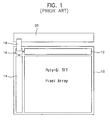
- poly-Si TFT LCD includes a data driving circuit 12 and a gate driving circuit 14 that are formed on a glass substrate 10 having a pixel array.
- a terminal part 16 is connected with an integrated printed circuit board (PCB) 20 using a film cable 18.
- PCB printed circuit board
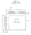
- amorphous-Si TFT LCD has a data driving chip 34 formed on a flexible printed circuit board 32 in a manner of COF (Chip-On-Film).
- a data printed circuit board 36 is connected with a data line terminal of the pixel array through the flexible PCB 32.
- a gate driving chip 40 is formed on a flexible PCB 38 in a manner of COF.
- a gate PCB 42 is connected with a gate line terminal through the flexible PCB 40.
- US Patent No. 5,517,542 which forms the basis for the preamble of claim 1, discloses a technique for an a-Si TFT gate driving circuit formed on a glass substrate.
- a shift register of the gate driving circuit uses three clock signals. Each stage of the shift register two clock signals of three clock signals, is enabled with an output signal of previous stage as an input signal, and maintains the disable state by feed backing an output of the second next stage.
- Each stage in the US Patent provides a voltage applied to gate of pull-down transistor in a capacitor charge manner in order to maintain the disable status.
- the above US patent employs a power supply circuit elevating a VDD in proportional to the increase in the threshold voltage of the a-Si TFT LCD in order to prevent an error operation due to the increase in the threshold voltage.
- the first power voltage is a turn off voltage (VOFF, VSS) and the second power voltage is a turn on voltage (VON, VDD).
- each stage further may comprises a turn-on preventing means connected to the input node of the pull-down means, wherein the turn-on preventing means connects the first power voltage to the input node of the pull-down means in response to the output signal of the output terminal to prevent the pull-down means from being turned on.
- the turn-on preventing means may comprises an NMOS transistor of which drain is connected to the input node of the pull-down means, gate is connected to the output terminal and source is connected to the first power voltage.
- the pull-up driving means may have a capacitor connected between the input node of the pull-up means and the output terminal; a first transistor of which drain and gate are commonly connected to the input terminal and source is connected to the input node of the pull-up means; a second transistor of which drain is connected to the input node of the pull-up means, gate is connected to the input node of the pull-down means and source is connected to the first power voltage ; and a third transistor of which drain is connected to the input node of the pull-up means, gate is connected to an output signal of a next stage and source is connected to the first power voltage.
- the pull-down driving means may comprises: a fourth transistor of which drain is connected to the second power voltage, gate is connected to the output signal of the next stage and source is connected to the input node of the pull-down means; and a fifth transistor of which drain is connected to the input node of the pull-down means, gate is connected to the input signal and source is connected to the first power voltage.
- the floating preventing means may have a sixth transistor of which drain and gate are connected to the second power voltage and source is connected to the input node of the pull-down means, wherein the sixth transistor has a size smaller sufficiently than the fifth transistor.
- a size ratio of the fifth transistor to the sixth transistor is approximately 20: 1.
- the external connection terminal connected to the shift register may comprises five terminals of a first clock signal input terminal, a second clock signal input terminal, a start signal input terminal, a first power voltage input terminal and a second power voltage input terminal.
- a size ratio of the fifth transistor to the seventh transistor may be approximately 2:1.
- the a pull-up driving means may be provided with a capacitor of which one end is connected to an input node of the pull-up means and the other end is connected to the output terminal, and a discharging means for forcibly discharging the capacitor depending on an external input control signal, the pull-up driving means may turn on the pull-up means by charging the capacitor and may turn off the pull-up means by forcibly discharging the capacitor.
- T he pull-up driving means may comprise: a capacitor connected between the input node of the pull-up means and the output terminal; a first transistor of which gate is connected to the input signal, drain is connected to a second power voltage and source is connected to the input node of the pull-up means; a second transistor of which drain is connected to the input node of the pull-up means, gate is connected to the input node of the pull-down means and source is connected to the first power voltage; a third transistor of which drain is connected to the input node of the pull-up means, gate is connected to the output signal of the next stage and source is connected to the first power voltage; and a fourth transistor of which drain is connected to the input node of the pull-up means, source is connected to the first power voltage and gate forcibly discharges the capacitor which receives the external input control signal.
- T he external input control signal may have a voltage level capable of turning on the transistor when a power is applied and turning off the transistor before the start signal is applied to the first stage. Also, the external input control signal has a voltage level capable of turning off the transistor while the start signal is applied to the first stage and an output of a last shift register is generated, and turning on the transistor after the output of the last shift register is generated, thereby discharging the capacitor of the last shift register.
- the pull-up driving means may comprises: a capacitor connected between the input node of the pull-up means and the output terminal; a first transistor of which gate is connected to the input signal, drain is connected to a second power voltage and source is connected to the input node of the pull-up means; a second transistor of which drain is connected to the input node of the pull-up means, gate is connected to the input node of the pull-down means and source is connected to the first power voltage ; and a third transistor of which drain is connected to the input node of the pull-up means, gate is connected to the output signal of the next stage and source receives the external input control signal to forcibly discharge the capacitor.
- the sources of the second transistor and the third transistor may be commonly connected to each other.
- the external input control signal maintains a low state simultaneously with an application of a power to thereby forcibly discharge the capacitor, and maintains a high state before the start signal applied to the first stage is generated.
- the external input control signal may have a voltage level capable of turning on the third transistor when a power is applied, and turning off the third transistor before the start signal is applied to the first stage.
- the turning on voltage level is the second power voltage
- the turning off voltage level is the first power voltage.
- the second power voltage may be above a threshold voltage capable of turning on the third transistor even when the first power voltage is applied to the gate terminal of the third transistor and less than the first power voltage.
- the external input control signal has a voltage level capable of turning off the transistor while the start signal is applied to the first stage and an output of a last shift register is generated, and turning on the transistor after the output of the last shift register is generated, thereby discharging the charge accumulated in the capacitor of the last shift register.
- the LCD may compris e a display cell array circuit, a data driving circuit and a gate driving circuit formed on a transparent substrate.
- the display cell array circuit has multiple data lines and multiple gate lines, each of the display cell arrays connected to a corresponding pair of data line and gate line.
- the gate driving circuit may have a first shift register comprising multiple stages connected one after another to each other, the multiple stages having a first stage in which a start signal is coupled to an input terminal, for sequentially selecting the multiple gate lines using an output signal of each stage.
- the data driving circuit may compris e multiple data line blocks and a second shift register, each of the data line blocks comprising multiple driving transistors each of which drain and source are connected between a data input terminal and the data line and gate is commonly connected to a block selection terminal, the second shift register comprising multiple stages connected one after another to each other, the multiple stages having a first stage in which a data block selection start signal is coupled to an input terminal, for sequentially selecting the multiple data line blocks using an output signal of each stage.
- the LCD further may comprise a flexible PCB on which an integral control and data driving chip is mounted, for providing the input terminals of the gate and data driving circuits with a control signal and a data signal.
- the first and second shift registers according to claim 1 employ the shift register for accomplishing the first object of the present.
- a duty period of the first and second clock signals applied to the first shift register is greater than a period of a duty period of the first and second clock signals applied to the second shift register multiplied by a number of the data line blocks.
- the transparent substrate may be connected to the flexible PCB through an external connection terminal.
- the external connection terminal has; five terminals connected to the data driving circuit of a first clock signal input terminal, second clock signal input terminal, scan start signal input terminal, first power voltage input terminal and second power voltage input terminal ; and three control terminals of first clock signal input terminal, second clock signal input terminal and block selection start signal input terminal ; and multiple data input terminals all of which are connected to the data driving circuit.
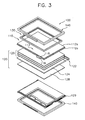
- FIG. 3 is a disassembled perspective view of an a-si TFT LCD in accordance with the present invention.
- an LCD 100 includes an LCD panel assembly 110, a backlight assembly 120, a chassis 130 and a cover 140.
- the LCD assembly 110 includes an LCD panel 112, a flexible PCB 116 and an integral control and data driving chip 118.
- the LCD panel 112 includes a TFT substrate 112a and a color filter substrate 112b.
- On the TFT substrate 112a there are disposed a display cell array circuit, a data driving circuit, a gate driving circuit and an external connection terminal.
- the TFT substrate 112a faces with the color filter substrate 112b. Liquid crystal is injected between the TFT substrate 112a and the color filter substrate 112b, and an injection inlet of liquid crystal is then sealed.
- the integral control and data driving chip 118 mounted on the flexible PCB 116 is connected with circuits formed on the TFT substrate 112a through the flexible PCB 116.
- the flexible PCB 116 provides the data driving circuit and the gate driving circuit of the TFT substrate 112a with data signals, data timing signals, gate timing signals and gate driving voltages.
- the backlight assembly 120 includes a lamp assembly 122, a light guiding plate 124, a series of optical sheets 126, a reflector plate 128 and a mold frame 129.
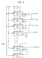
- a display cell array circuit 150 On the TFT substrate 112a of the present invention, there are arranged a display cell array circuit 150, a data driving circuit 160, a gate driving circuit 170, an external connection terminal 162 and 163 for the data driving circuit 170, which are formed during the formation of TFTs.
- the display cell array circuit 150 includes an m-number of data lines DL1-DLm extended along the column direction and an n-number of gate lines GL1-GLn extended along the row direction.
- an example of 2 inches-LCD panel having a resolution of 525(176 ⁇ 3) ⁇ 192 corresponding to numbers of the gate lines and data lines.
- Switching transistors ST are formed at the cross points of the data lines and the data lines.
- Switching transistor STi has a drain connected to a data line DLi and a gate connected to a gate line GLi.
- Source of the switching transistor STi is connected to a transparent pixel electrode PE.
- Liquid crystal LC is arranged between the transparent pixel electrode PE and a transparent common electrode CE.
- a voltage applied between the transparent pixel electrode PE and the transparent common electrode CE controls the alignment of liquid crystal molecules, thus light amount passing through the liquid crystal molecules is controlled and thereby gray scales for respective pixels are displayed.
- the data driving circuit 160 includes a shift register 164 and 568 switching transistors SWT.
- the 528 switching transistors SWT form eight data line blocks BL1-BL8 per sixty-six switching transistors.
- sixty-six input terminals are commonly connected to an external input terminal 163 consisting of sixty-six data input terminals and sixty-six output terminals are connected to the corresponding sixty-six data lines. Also, a block selection terminal is connected to a corresponding one output terminal of eight output terminals of the shift register 164.
- the 528 switching transistors SWT is made of a-Si TFT MOS transistor of which source is connected to corresponding data line, drain is connected to a corresponding input terminal among 66 number of data input terminals, and gate is connected to block selection terminal.
- 528 data lines are divided into eight blocks each having sixty-six data lines and the eight blocks are each selected sequentially by eight block selection signals.
- the shift register 164 receives a first clock signal (“CKH”), a second clock signal (“CKHB”) and a block selection start signal (“STH”).
- the output terminals of the shift register 164 are connected to the block selection terminals of corresponding lines blocks.
- the shift register 164 includes nine stages SRH1 to SRH9 subordinated to one after another.
- the output terminal "OUT" of each stage is connected to the input terminal "IN” of the next stage.
- the nine stages have eight stages SRH1 to SRH8 corresponding to data line blocks and one dummy stage SRH9.
- Each stage has input terminal IN, output terminal OUT, control terminal "CT”, clock signal input terminal "CK”, first power voltage terminal "VSS” and second power voltage terminal “VDD”.
- the eight stages SRH1 to SRH8 provide the block selection terminals of respective data line blocks BL1 to BL8 with the block selection start signals DE1 to DE8, respectively.
- the block selection start signals are the enable signals for respective line blocks.
- Odd stages SRH1, SRH3, SRH5, SRH7, SrH9 receive the first clock signal "CKH" and even stages SRC2, SRC4, SRH6, SRH8 receive the second clock signal.
- the first clock signal CKH and the second clock signal CKHB have a phase opposite to each other. Duty periods of the first and second clock signals CKH and CKHB are set to be less than 1/66ms.
- the output signal of the next stage to a present stage is input to the control terminal CT of the present stage as a control signal.
- the control signal that is input to the control terminal CT is delayed by the duty period of the output signal itself.
- Dummy stage SRH9 is used for providing the control terminal CT of the previous stage SRH8 with a control signal.
- the gate driving circuit 170 has a single shift register.
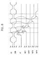
- the shift register 170 of FIG. 6 includes multiple stages SRC1 to SRC4 subordinated to one after another. In other words, the output terminal "OUT" of each stage is connected to the input terminal IN of the next stage.
- the stages consist of 192 stages SRC1 to SRC192 corresponding to gate lines and one dummy stage SRC193. Each stage has input terminal IN, output terminal OUT, control terminal CT, clock signal input terminal CK, first power voltage terminal VSS and second power voltage terminal VDD.
- the start signal is a pulse signal synchronized with a vertical synchronous signal.
- Output terminals OUT1 to OUT192 of respective stages are connected to respective corresponding gate lines.
- To odd stages SRC1 and SRC3 is supplied the first clock signal CK and to even stages SRC2 and SRC4 is supplied the second clock signal CKB.
- the first clock signal CK has an opposite phase to the second clock signal CKB.
- the first and second clock signals CK and CKB have a duty period of 16.6/192ms.
- the duty period of the clock signal of the shift register 170 for the gate driving circuit is 8 times and more.
- the output signals OUT2, OUT3 and OUT4 of the next stages SRC2, SRC3 and SRC 4 to present stages SRC1, SRC2 and SRC3 are input to the control terminal CT of the present stages SRC1, SRC2 and SRC3 as a control signal.
- the control signal that is input to the control terminal CT is delayed by the duty period of the output signal itself.
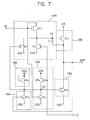
- each stage of the shift registers 164 and 170 includes pull-up section 180, a pull-down section 182, a pull-up driving section 184, pull-down driving section 186, a floating preventing section 188 and a turn-on preventing section 190.
- the pull-up section 180 includes a pull-up NMOS transistor NT1 of which drain is connected to a clock signal input terminal CK, gate is connected to a first node N1 and source is connected to an output terminal OUT.
- the pull-down section 182 includes a pull-down NMOS transistor NT2 of which drain is connected to an output terminal OUT, gate is connected to a second node N2 and source is connected to a first power voltage VSS.
- the pull-up driving section 184 includes a capacitor C and an NMOS transistor NT3 to NT5.
- the capacitor C is connected between the first node N1 and the output terminal OUT.
- Transistor NT3 has a drain and gate commonly connected to the input terminal IN and a source connected to the first node "N1".
- Transistor NT4 has a drain connected to the first node N1, a gate connected to the second node “N2: and a source connected to the first power voltage VSS.
- Transistor NT5 has a drain connected to the first node N1, a gate connected to the control terminal "CT" and a source connected to the first power voltage VSS.
- the pull-down driving section 186 includes two NMOS transistors NT6 and NT7.
- Transistor NT6 has a drain connected to the second power voltage VDD, a gate connected to the control terminal CT and a source connected to the second node "N2".
- Transistor NT7 has a drain connected to the second node "N2", a gate connected to the input terminal "IN” and a source connected to the first power voltage VSS.
- the floating preventing section 188 includes an NMOS transistor NT8 of which drain and gate are commonly connected to the second power voltage VDD and a source is connected to the second node N2.
- Transistor NT8 has a size smaller sufficiently than transistor NT7, for example, has a size ratio of 1:20.
- the turn-on preventing section 190 includes an NMOS transistor NT9 of which drain is connected to the second node N2, gate is connected to the output terminal OUT and source is connected to the first power voltage VSS.
- Transistor NT9 has a size ratio of 1:2 to transistor NT7.
- the first stage SRC1 delays a high level period of the first clock signal CK in response to the front edge of the scan start signal ST for a predetermined time of Tdr1 to thereby output a delayed output signal OUT1.
- the active period of the scan start signal ST has a phase faster by 1/4 than the high level period of the first clock signal CK.
- the active period of the scan start signal ST is divided into a set up time Ts1 from a front edge of a pulse, i.e., a rising edge and a hold time Ts2 to a rear edge of a pulse, i.e., a falling edge.
- the front edge of the output signal OUT1 has a front edge, i.e., rising edge delayed by a certain time of approximately 2-4 ⁇ s from the start point of the hold time Ts2.
- active period of the first clock signal CK i.e., high level period is delay-output by a time of Tdr1 to the output terminal OUT.
- This delay characteristic is due to the fact that the capacitor C of the pull-up driving section 184 starts to be charged through the transistor NT3 in a state where the transistor NT4 is turned off at the front edge of the start signal ST and the pull-up transistor NT1 is turned on after the charged voltage of the capacitor C becomes higher than a threshold voltage between the gate and the source of the pull-up transistor NT1, whereby the high level period of the first clock signal CK is generated at the output terminal.
- this output voltage is bootstrapped at the capacitor C and thereby the gate voltage of the pull-up transistor NT1 rises over the turn-on voltage VDD. Accordingly, the pull-up transistor NT1 of NMOS transistor maintains a full turn-on state.
- the pull-down driving section 186 since the transistor NT7 is turned on at the front edge of the start signal ST in a state where the transistor NT6 is turned off, a potential of the second node N2 is dropped to the first power voltage VSS.
- the transistor NT8 of the floating preventing section 188 maintains the turn on a state while since a size of the turn on transistor NT7 is larger 20 times than the transistor NT8, the second node N2 is voltage-dropped to the first power voltage VSS from the second power voltage VDD. Therefore, the pull-down transistor NT2 is transferred from the turn-on state to the turn-off state.
- the transistor NT9 of the turn on the preventing section 190 is turned on, so that a capability for driving the second node N2 using the first power voltage VSS increases approximately 50%.
- rising of the second node voltage can be prevented by a parasitic capacitance between drain and source of the pull-down transistor upon the rising transition of the output signal.
- an error operation of the pull-down transistor in which the pull-down transistor is turned on upon the rising transition of the output signal may be prevented.
- the output signal OUT1 of the output terminal OUT is delay-generated by the duty period of the first clock signal CK.
- the pull-up transistor NT1 is turned off and the pull-down transistor NT2 is turned on, so that a voltage of the output terminal OUT is dropped from the turn on voltage VON to the turn off voltage VOFF of the second power voltage VDD.
- the second node N2 maintains the second voltage VDD-biased state through the transistor NT8 and the first node N1 maintains the first power voltage VSS-biased state through the transistor NT4 maintaining the turn on state.
- a threshold voltage of the transistors NT2 and NT4 due to the long term use rises, since a potential of the second node N2 is maintained at the second power voltage VDD, a stable operation can be secured without an error operation such as the pull-down transistor NT2 being turned off.
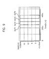
- Respective stages SRC1-SRC4 are operated in the same manner with the aforementioned method and thus output signals OUT1 to OUT4 are sequentially and stably generated as shown in FIG. 9 .
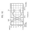
- FIG. 10 shows a simulation result of when a gate line load 30pF for a 2 inches panel is connected to the aforementioned shift register of the present invention.
- the result shows that output signals OUT2 and OUT 3 were delayed with respect to the clock signals CK and CKB, respectively.
- a rising time and a falling time of the output signals were approximately 1.5 ⁇ s
- a delay rising time Tdr and a delay falling time Tdf of from the clock signal were approximately 0.3 ⁇ s.
- FIG. 11 shows a layout of an external connection terminal part that is provided in a shift register of a gate driving circuit integrated on an LCD panel of the present invention.
- Right side of the layout is a TFT side and left side of the lay-out is a film cable side.
- the shift register of the present invention needs only five external connection terminals of a start signal (ST) input terminal, a first clock signal input terminal CK, a second clock signal input terminal CKB, a first power voltage terminal VOFF or VSS and a second power voltage terminal VON or VDD. Accordingly, a space occupied by the terminal part 172 on the glass substrate can be decreased.
- ST start signal
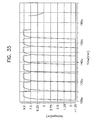
- FIGS. 12 to 14 are waveforms comparing an output characteristic of a conventional shift register employing a pull-down control technique using a capacitor with that of a shift register of the present invention.
- FIG. 12 is a graph for comparing a voltage waveform of the second node N2. As shown in FIG. 12 , the present invention corresponding to the solid line maintains more stable low level state than the conventional art of the dotted line in a sector "A".
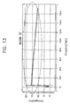
- FIG. 13 is a graph for comparing a state variation in the high level of the second node N2.
- the conventional art of the dotted line shows that the level is decreased according to the time elapse while the present invention of the solid line shows that a constant level is maintained regardless of the time elapse. This is because the present invention always maintains a supply state of the power voltage VDD through the floating preventing section.
- FIG. 14 is a graph for comparing waveforms of output signals in the output terminals. It is shown that an output signal waveform of the solid line corresponding to the present invention maintains more stable high level state in the active state (that is, high level state) compared with an output signal waveform of the broken line corresponding to the conventional art. It is also known that the present invention maintains a stable low level-biased state in the non-active state (that is, low level state).
- FIG. 15 is a circuit diagram of each stage of the shift registers in the data driving circuit and the gate driving circuit.
- each stage of the shift registers 164 and 170 includes a pull-up section 190, a pull-down section 192, a pull-up driving section 194 and a pull-down driving section 196.
- the pull-up section 190 includes a pull-up NMOS transistor NT11 whose drain is connected with a clock signal input terminal CK, gate is connected with a third node N3 and source is connected with an output terminal OUT.
- the pull-down section 192 includes a pull-down NMOS transistor NT12 whose drain is connected with the output terminal OUT, gate is connected with a fourth node N4 and source is connected with a first power voltage VSS.
- the pull-up driving section 194 includes a capacitor C and NMOS transistors NT13, NT14 and NT15.
- the capacitor C is connected between the third node N3 and the output terminal OUT.
- the transistor NT13 includes drain connected with a second power voltage VDD, gate connected with an input terminal IN and source connected with the third node N3.
- the transistor NT14 includes drain connected with the third node N3, gate connected with a control terminal CT and source connected with the first power voltage VSS.
- the transistor NT15 includes drain connected with the third node N3, gate connected with the fourth node N4 and source connected with the first power voltage VSS.
- the transistor NT13 has a size approximately two times larger than the transistor NT15.
- the pull-down driving section 196 includes two NMOS transistors NT16 and NT17.
- the transistor NT16 includes drain and gate both of which are commonly connected with the second power voltage VDD, and source connected with the fourth node N4.
- the transistor NT17 includes drain connected with the fourth node N4, gate connected with the third node N3 and source connected with the first power voltage VSS.
- the transistor NT16 has a size 16 times larger than the transistor NT17.
- first and second clock signals CK and CKB and scan start signal ST are supplied to the shift register 170, the first stage of the shift register 170 delays a high level period of the first clock signal CK for a predetermined time of Tdr1 in respond to a front edge of the scan start signal ST, to thereby output a delayed output signal OUT1.
- An active period of the scan start signal ST has a phase faster by approximately 1/4 than the high level period of the first clock signal CK.
- the active period of the scan start signal ST is divided into a set up time Ts1 from a front edge of a pulse, i.e., a rising edge and a hold time Ts2 to a rear edge of the pulse, i.e., a falling edge.
- an output signal OUT1 has a front edge, i.e., a rising edge delayed by a certain time of approximately 2-4 ⁇ s from a start point of the hold time Ts2.
- the active period of the first clock signal CK i.e., high level period is delay-output by a time of Tdr1 to the output terminal OUT.
- This delay characteristic is due to the fact that the capacitor C of the pull-up driving section 194 starts to be charged through the transistor NT13 in a state where the pull-up transistor NT11 is turned on after the charged voltage of the capacitor C becomes higher than a threshold voltage or more between the gate and the source of the pull-up transistor NT11, whereby the high level period of the first clock signal CK is generated at the output terminal.
- this output voltage is bootstrapped at the capacitor C and thereby the gate voltage of the pull-up transistor NT11 rises over the turn-on voltage VDD. Accordingly, the pull-up transistor NT11 of NMOS transistor maintains a full turn-on state. At this time, since the transistor NT13 has the size two times larger than the transistor NT15, even if the transistor NT15 is turned on by the start signal ST, the transistor NT11 is transferred from the turn-off state to the turn-on state.
- the pull-down driving section 196 since the transistor NT17 is turned off by an input signal, a potential of the fourth node N4 rises to the second power voltage VDD to thereby turn on the transistor NT12. Accordingly, the voltage of the output signal in the output terminal OUT is in the state of the first power voltage VSS. At this time, since the transistor NT17 is turned on by the start signal ST, the potential of the fourth node N4 is dropped to the first power voltage VSS. After that, since the transistor NT17 has a size 16 times larger than the transistor NT16, even if the transistor NT16 is turned on, the fourth node N4 continues to maintain the state of the first power voltage VSS. Accordingly, the pull-down transistor NT12 is transferred from the turn-on state to the turn-off state.
- the output signal OUT1 of the output terminal OUT is delay-generated by the duty period of the first clock signal CK.
- the transistor NT14 is turned on.
- a potential of the third node N3 is dropped to the first power voltage VSS faster than a drop rate where only the transistor NT15 is turned on since the transistor NT14 has a size twice times larger than the transistor NT16. So, the pull-up transistor NT11 is turned off and the pull-down transistor NT12 is turned on, so that a voltage of the output terminal OUT is dropped from the turn-on voltage VON to the turn-off voltage VOFF of the second power voltage VDD.
- the fourth node N4 maintains the second power voltage VDD-biased state through the transistor NT16 and the third node N3 maintains the transistor NT15 that is held at the turn-on state in the first power voltage VSS-biased state.
- the potential of the fourth node N4 is maintained at the second power voltage VDD, a stable operation can be secured without anxiety of an error operation.
- Each of the stages is operated by the aforementioned manner, so that output signals OUT1, OUT2, OUT3 and OUT4 are sequentially and stably generated as shown in FIG. 17 .
- the second embodiment arranges the transistors NT15 and NT17 in a latch type to thereby maintain a stable state at the third node N3 and the fourth node N4. Also, the second embodiment not only removes two transistors but decrease size of the transistor, thereby capable of decreasing the area occupied by the shift register within the LCD panel 10%. Moreover, compared with the first embodiment, the second embodiment makes it possible to secure a stable operation regardless of the pulse width of the scan start signal ST.
- the first embodiment starts to discharge the capacitor before clock signal is input in a case where the pulse width of the scan start signal ST is narrower than that of the clock signal.
- the pull-down transistor is turned on, so that any output is not generated.
- an output signal is not shifted to a next terminal, an impossible state in the operation may occur.
- the second embodiment latches the scan start signal ST, a stable operation is possible regardless of narrowness and wideness of the pulse width.
- FIG. 18 is waveforms of first and second clock signals in accordance with another embodiment of the present invention and FIG. 19 is output waveforms of respective stages.
- the first and second clock signals CK and CKB are supplied to each stage of the shift registers 164 and 170. Specifically, to odd stages is supplied the first clock signal CK and to even stages is supplied the second clock signal CKB.
- the first clock signal CK has an opposite phase to the second clock signal CKB.
- high level periods of the second clock signals CK and CKB are generated at the output terminal OUT of the respective stages as an output signal.
- a constant phase difference P1 is placed between the high level periods that are respectively generated at the first clock signal CK and the second clock signal CKB that are supplied to the respective stages.
- the high level period of the first clock signal CK is supplied to the odd stage and the high level period of the second clock signal CKB is then supplied to the even stage after an elapse of a certain time.
- a constant phase difference P2 is generated between high periods of output signals OUT1, OUT2, OUT3, OUT4, and OUT5 that are generated at the respective stages.
- high level periods of the output signals OUT1, OUT3, OUT5 of the odd stages to which the first clock signal CK is supplied are generated and a predetermined time has been elapsed, high level periods of the output signals OUT2 and OUT4 of the even stages to which the second clock signal CKB is supplied are generated. Accordingly, there can be prevented an overlap phenomenon that the falling transfer of the output signal of each stage is overlapped with the rising transfer of the output signal of the next stage.
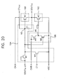
- FIG. 20 is a circuit diagram of each stage in the shift register in accordance with a third embodiment of the present invention and FIG. 21 is a timing diagram for illustrating the driving waveform of the shift register of FIG. 20 .
- each stage of the shift registers 170 in accordance with the third embodiment of the invention includes a pull-up section 190, a pull-down section 192, a pull-up driving section 194 and a pull-down driving section 196.
- the pull-up section 190 includes a pull-up NMOS transistor M2 of which drain is connected to a clock signal input terminal CK, gate is connected to a fifth node N5 and source is connected to an output terminal GOUT.
- the pull-down section 192 includes a pull-down NMOS transistor M3 of which drain is connected to the output terminal OUT, gate is connected to a sixth node N6 and source is connected to a first power voltage VSS.
- the pull-up driving section 194 includes a capacitor C and NMOS transistors M1 and M4.
- the capacitor C is connected between the fifth node N5 and the output terminal OUT.
- Transistor M1 has a drain and gate commonly connected to an input signal and a source connected to an input node of the pull-up section 190 via the fifth node N5. If it is assumed that the stage shown in FIG. 20 is the first stage, the drain and gate connected to each other are commonly connected to the input signal while it is assumed that the stage shown in FIG. 20 is the second stage or more, the drain and gate connected to each other are commonly connected to an output terminal of a previous stage to receive a previous carry signal.
- Transistor M4 has a drain connected to the input node of the pull-up section 190, a gate connected to an output signal of a next stage and a source connected to the first power voltage VSS.
- the pull-down driving section 196 includes two NMOS transistors M5 and M6, and performs an inverter operation.
- Transistor M5 has a drain and gate commonly connected to a second power voltage VDD and a source connected to the sixth node "N6".
- Transistor M6 has a drain connected to the sixth node "N6", a gate connected to the fifth node "N5" and a source connected to the first power voltage VSS.
- the transistor M5 has a size 16 times larger than the transistor M6.
- a signal CT1 [n+2] of the next stage is applied to gate of the transistor M4 as the signal CT, the transistor M4 is turned on, so that the fifth node N5 is discharged to the first power voltage (VSS) level.
- the transistor M3 should be turned off. If the transistor M3 is not sufficiently turned off, a leakage current is generated at a path between the transistor M2 and the transistor M3, so that power consumption increases.
- the transistors M5 and M6 invert the gate voltage of the transistor M2, i.e., the voltage of the fifth node N5, to thereby prevent the transistors M2 and M3 from being turned on at the same time.
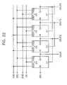
- FIG. 22 is a circuit diagram for illustrating an a-TFT LCD gate driving circuit using the shift register in accordance with the second embodiment of the present invention
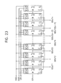
- FIG. 23 is a circuit diagram for illustrating an a-TFT LCD gate driving circuit using the shift register in accordance with the third embodiment of the present invention.
- the foregoing stages of FIG. 15 are connected in series above the number of the gate lines to carry out the operation of the gate driving circuit. Then, because they need a total of five transmission lines (VDD, VSS, CKV, CKVB, STV) as the external inputs, and seven transistors every stage, i.e., they need too many transistors and transmission lines, there exists a spatial limitation for a layout thereof on a-TFT LCD substrate.
- the inverting circuit 196 including the transistors NT16 and NT17 for making a level capable of turning off the pull-down NT12, a condition in which the two transistors NT16 and NT17 are simultaneously turned on is generated during its operation, so that a problem on the power consumption occurs. Since it is difficult that VSS is appleid to the pull-down section NT12 as the turn-off voltage, there occurs a leakage current problem at a path between the pull-up section NT11 and the pull-down section NT12.
- the fourth node N4 is in a high state at an initial state, there occurs a limit on the circuit in that the charging of the capacitor becomes difficult in turn-on state of the transistor NT15. So, unless the sizes of the transistors NT13, NT14, NT16 and NT17 are precisely adjusted, there occurs an operation failure problem in that the signal "IN" is not charged in the capacitor because of turn-on of the transistor NT15.
- the shift register disclosed in the third embodiment of the present invention it is possible to apply less number of transistors and transmission lines to a-TFT LCD substrate. Accordingly, it is possible to provide a-TFT gate driving circuit having easy design characteristic and capable of solving the problems occurring on the operation.
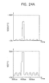
- FIGS. 24A and 24B are simulation results of gate output waveforms of when the output GOUT of the next stage is used as an input of the node CT and of when the signal CT1 of the stage after the next stage is used as an input of the node CT.
- CT1 voltage is coupled to CK in the third embodiment of the present invention, it is possible to maintain the coupling voltage of CT1 at VSS or less, thereby preventing an error operation of the transistor M2.
- the third embodiment of the present invention it is possible to remove the discharge transistor NT15 shown in FIG. 15 .
- error operation on the circuit due to the transistor NT15 can be prevented, and the number of the transistors in the shift register can be simplified to 6 in number.
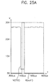
- FIGS. 25A and 25B are waveforms of gate signals respectively outputted from the gate drivers in accordance with the second embodiment and the third embodiment of the present invention. In particular, they describe simulation results of CT2 waveform for turning off the transistor M3.
- CT2 by using CKB signal which reaches a low state when transistor M2 is turned on, instead of the conventional second power voltage VDD, when the transistor M2 is turned on and accordingly signal OUT1 is generated, CT2 necessarily reaches the first power voltage level to thereby turn off the transistor M3 and remove an occurrence of over current.
- the third embodiment of the invention removes error operation or over current occurrence of the conventional a-TFT gate driving circuit, thereby securing stability and superior characteristic compared with the second embodiment.
- the third embodiment enables to remove transmission lines for one transistor and further second power voltage VDD that are essential elements for the consititution of the shift register, so that a-TFT gate driving circuit having a high integrity is provided.
- the number of the transistors can be decreased from 7 to 6, and the number of the external input terminals can be decreased from 5 to 4, thereby securing the circuit stability and realizing a high integrity.
- the respective stages are fabricated as shown in FIG. 15 , connected in series above the number of the gates as shown in FIG. 22 .
- the respective stages carries out the function of gate drive IC.
- the circuit is low in the reliability. In other words, over current flows into the signal transmission line VSS, CKV or CKVB, so that the signal transmission line is open, or overload is applied to the circuit, whereby system has broken down.
- the capacitor C of the node N3 causes such the problems. This phenomenon occurs when nondesired charge is accumulated in the capacitor by static electricity at multiple stages, when an initial external power is applied, the charge is accumulated in the capacitor at unstable power and unstable signal state, or CKV and CKVB are applied to the circuit and multiple stages are simultaneously operated.
- transistor NT11 of each stage carries out a charging process of the load capacitor applied to GOUT.
- discharging process is carried out by the transistor NT12. If this operation is simultaneously carried out at the multiple stages, overcurrent flows into the signal transmission line VSS, CKV or CKVB.
- This overcurrent is generated during one frame in which shifting operation is completed, for instance, for 16.7 msec in 60 Hz, so that heat is generated in the transmission line of VSS having a resistance during the time and thus there occurs a phenomenon in which the transmision line is melted by the heat and is opened.
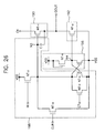
- FIG. 26 is a circuit diagram of each stage in the shift register in accordance with a fourth embodiment of the present invention and FIG. 27 is driving waveforms of the circuit of FIG. 26 .
- each stage of FIG. 26 is provided with a transistor for discharge alone for discharging the charge accumulated in the capacitor.
- each stage of the shift registers 170 in accordance with the present embodiment includes a pull-up section 190, a pull-down section 192, a pull-up driving section 198 and a pull-down driving section 196.
- the pull-up section 190, the pull-down section 192 and the pull-down driving section 196 are the same as those of FIG. 15 , their description will be omitted.
- the pull-up driving section 198 includes a capacitor C and an NMOS transistor NT13, NT14, NT15 and NT18. More particulary, the capacitor C is connected between the third node N3 and the output terminal OUT.
- Transistor NT13 has a drain connected to the second power voltage VDD, gate connected to an input terminal IN and a source connected to the third node N3.
- Transistor NT14 has a drain connected to the third node N3, gate connected to a control terminal CT and a source connected to the first power voltage VSS.
- Transistor NT15 has a drain connected to the third node N3, a gate connected to a fourth node N4 and a source connected to the first power voltage VSS.
- Transistor NT13 has a size approximately two times larger than the transistor NT15.
- Transistor NT18 has a source connected to the first power voltage VSS, a gate connected to an external input control signal (or clear signal) CLR and a drain for forcibly discharging the charge accumulated in the capacitor connected in parallel to the input node N3 of the pull-up section 190 using the drain.
- the external input control signal CLR is a signal for discharging the charge accumulated in the capacitor C to the first power voltage VSS, and maintains the second power voltage VDD state during a predetermined time such that the capacitor is discharged on an initial power on.
- the signal CLR is a signal of less than the threshold voltage, which allows a transistor to maintain the turn-off state during a time period when a picture is displayed, for instance, is a signal having the first power voltage (VSS) state.
- the external input control signal CLR maintains a high state simultaneously when a power Vin is applied, to thereby discharge the charged capacitor of the stage and then generate a vertical start signal STV.
- a means for discharging the charge accumulated in the capacitor of the pull-up driving section is independently provided, which can resolve an error operation due to the charge accumulated in the capacitor during the initial operation, or a damage problem of transmission line of an LCD panel, in particular, a-TFT LCD panel, thereby giving a TFT-LCD module having a high reliability.
- the current embodiment solves an error in the driving signal of the last gate line to thereby remove a line damage occurring in an end of a picture, so that there can be provided a TFT-LCD module provided with a gate driving circuit made of a functionally stable a-TFT.
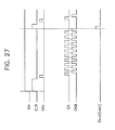
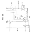
- FIG. 28 is a circuit diagram of each stage in the shift register in accordance with a fifth embodiment of the present invention and FIG. 29 is driving waveforms of the circuit of FIG. 28 .
- FIG. 28 is a circuit diagram for discharging the charge accumulated in the capacitor of the stage without adding a transistor for discharging alone.
- each stage of the shift registers 170 in accordance with the present embodiment includes a pull-up section 190, a pull-down section 192, a pull-up driving section 194 and a pull-down driving section 196.
- an external input control signal CLR is applied to source of transistor NT14 of the pull-up driving section 194.
- the external input control signal can be applied to source of transistor NT15 or to source of the transistor NT14 and transistor NT15 of which sources are commonly connected to each other.
- the current embodiment utilizes that a voltage of Vss and more is always applied to gate of transistor NT14.
- Vth is a threshold voltage of transistor NT14
- a voltage of Vss2 having a condition of Vss2 ⁇ Vss-Vth is applied to turn on the transistor NT14, thereby carrying out the discharging operation which forcibly lowers the charged voltage of the capacitor to the voltage level of Vss2.
- the external input control signal CLR maintains a low state (Vss2) simultaneously with an application of a power, to thereby discharge the charge accumulated in the capacitor of the stage, and then the external input control signal CLR reaches a high state before STV signal is generated.
- the two signals CKV and CKVB are in a low state when the external input control signal CLR is in the low state (Vss2).
- an external input control signal is supplied to source of a transistor of the pull-up driving section so as to discharge the charge accumulated in the capacitor, which can resolve an error operation due to the charge accumulated in the capacitor during the initial operation, or a damage problem of transmission line of an LCD panel, thereby giving a TFT-LCD module having high reliability.
- the present embodiment solves an error in the driving signal of the last gate line to thereby remove a line damage occurring in an end of an image, so that there can be provided a TFT-LCD module provided with a gate driving circuit made of a functionally stable a-TFT.
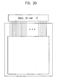
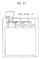
- the data driving circuit 160 of the present invention employs not a simultaneous operative manner of whole channels (see FIG. 30 ) but a block driving method (see FIG. 31 ).
- the block driving using a switching transistor can remarkably decrease the number of video channels that are provided to an LCD panel from the data driving chip.
- the block driving renders the charge time of the pixels to decrease. But, since a small sized panel of 2 inches can have a sufficient line time compared with the monitor for notebook computer or desk-top computer, it is possible to employ the block operation.
- a possible charge time is 7 ⁇ 8 ⁇ s upon considering a load and a delay depending on the panel size. Accordingly, upon considering a data driving chip having the same driving capability, 2"-sized panel has a charge time ten times or more than an UXGA level panel. Thus, although a block operation dividing the data line into ten blocks is performed, a 2"-sized panel has the same charge characteristic with an UXGA level panel.
- the present invention block-operates the data lines divided into eight blocks in the 2" sized panel. Therefore, if 528 video channels are divided into eight blocks, each block is assigned sixty-six channels. Thus, when compared with the simultaneous operation manner of 528 whole channels (see FIG. 20 ), it is possible to decrease a connection channel number from 528 channels to sixty-six channels.
- the present invention employs the block operation method of the data lines and integrates on a panel the data line driving circuit that sequentially selects respective blocks using the shift register, thereby remarkably decreasing the connection terminal number between the data driving chip and the panel to 1/8.
- embodiments in accordance with the present invention need only total connection terminals of sixty-six channel terminals, three data control terminals, five gate control terminals and one common voltage terminal (VCOM), seventy-five total connection terminals are necessary.
- VCOM common voltage terminal
- the present invention can decrease the number of the external connection terminals remarkably and the outer track size of the panel, so that the manufacturing cost is saved and the productivity and the price of the goods due to the slimmed panel are enhanced.
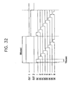
- the block operation method generates block selection signals DE1 to DE8 through the shift register 164 in order to sequentially enable 8 blocks at the active section.
- the present invention designs a 2" panel having a resolution of 176*192 to have a gate line active period of 86 ⁇ s and an active period of 10 ⁇ s for each block selection signal. Accordingly, it is possible to maintain a sufficient pixel charge characteristic upon the block operation.
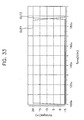
- FIGS. 33 to 35 show simulation results of gate line driving signal, data line block selection signal and pixel charge characteristic when a switching transistor (SWT) was designed to have a width of 4,000 ⁇ m and a length of 5 ⁇ s and a voltage of 20 V is applied.
- SWT switching transistor
- an active period of the gate line driving signal OUTi was 86 ⁇ s and an active period of the data line block signal DEi was 10 ⁇ s.
- the simulation result shows that the pixel charge rate of the block operation is 99% or more.
- the present invention uses two clock signals at a shift register mounted on the glass substrate of an LCD panel, so that it is possible to decrease the number of external connection terminals. Also, the second power voltage is continuously supplied to prevent the gate of the pull-down transistor from being floated in a disable state, so that it is possible to perform a stable operation regardless of the fluctuation in the threshold voltage of a-Si TFT LCD on a use of a long-term.
- the present invention employs the block driving method using the shift register in a small sized amorphous silicon TFT panel such as a 2" panel, so that the number of the connection channels decreases remarkably.
Claims (64)
- Registre à décalage (164 ; 174) possédant une pluralité d'étages (SRH1 à SRH9 ; SRC1 à SRC193), lequel registre à décalage (164 ; 174) émet successivement en sortie des signaux de sortie (OUT) vers des étages correspondants, chacun des étages (SRH1 à SRH9 ; SRC1 à SRC193) comprenant :un moyen de tirage au niveau haut (180 ; 190) destiné à fournir un signal d'horloge (CK) à une borne de sortie (OUT, GOUT) ;un moyen de commande du tirage au niveau haut (184 ; 194 ; 198) couplé à un noeud d'entrée (N1 ; N3 ; N5) du moyen de tirage au niveau haut (180 ; 190), pour activer le moyen de tirage au niveau haut (180 ; 190) en réponse à un signal d'entrée (IN) et pour désactiver le moyen de tirage au niveau haut (180 ; 190) en réponse à un signal de sortie (OUT, CT) d'un des étages suivants ;un moyen de tirage au niveau bas (182 ; 192) pour fournir une première tension d'alimentation (VSS) à la borne de sortie (OUT, GOUT) ; etun moyen de commande du tirage au niveau bas (186 ; 196) couplé à un noeud d'entrée (N2 ; N4 ; N6) du moyen de tirage au niveau bas (182 ; 192), pour désactiver le moyen de tirage au niveau bas (182 ; 192) en réponse au signal d'entrée (IN) et activer le moyen de tirage au niveau bas (182 ; 192) en réponse au signal de sortie (OUT, CT) d'un des étages suivants,caractérisé en ce que les étages impairs (SRH1, SRH3, SRH5, SRH7, SRH9 ; SRC1, SRC3, SRC5 à SRC193) parmi les étages reçoivent un premier signal d'horloge (CKH ; CK) et les étages pairs (SRH2, SRH4, SRH6, SRH8 ; SRC2, SRC4, SRC6 à SRC192) parmi les étages reçoivent un deuxième signal d'horloge (CKHB ; CKB) ayant une phase différente du premier signal d'horloge (CKH ; CK).
- Registre à décalage (164 ; 170) selon la revendication 1, dans lequel chacun des étages (SRH1 à SRH9 ; SRC1 à SRC193) comprend un outre un moyen de prévention du flottement (188) connecté au noeud d'entrée (N2 ; N4 ; N6) du moyen de tirage au niveau bas (182 ; 192), lequel moyen de prévention du flottement (188) fournit une deuxième tension d'alimentation (VDD) au noeud d'entrée (N2 ; N4 ; N6) du moyen de tirage au niveau bas (182 ; 192) pour empêcher le noeud d'entrée (N2 ; N4 ; N6) du moyen de tirage au niveau bas (182 ; 192) de flotter.
- Registre à décalage (164 ; 170) selon la revendication 2, dans lequel chacun des étages (SRH1 à SRH9 ; SRC1 à SRC193) comprend en outre un moyen de prévention de l'activation (190) connecté au noeud d'entrée (N2 ; N4 ; N6) du moyen de tirage au niveau bas (182 ; 192), lequel moyen de prévention de l'activation (190) fournit la première tension d'alimentation (VSS) au noeud d'entrée (N2 ; N4 ; N6) du moyen de tirage au niveau bas (182 ; 192) en réponse au signal de sortie (OUT) de la borne de sortie (OUT, GOUT) pour empêcher l'activation du moyen de tirage au niveau bas (182 ; 192).
- Registre à décalage (164 ; 170) selon la revendication 3, dans lequel le moyen de prévention de l'activation (190) comprend un transistor NMOS (NT9) dont le puits est connecté au noeud d'entrée (N2 ; N4 ; N6) du moyen de tirage au niveau bas (182 ; 192), la grille est connectée à la borne de sortie (OUT, GOUT) et la source est connectée à la première tension d'alimentation (VSS).
- Registre à décalage (164 ; 170) selon la revendication 2, dans lequel le moyen de commande du tirage au niveau haut (184 ; 194 ; 198) comprend :une capacité (C) montée entre le noeud d'entrée (N1 ; N3 ; N5) du moyen de tirage au niveau haut (180 ; 190) et la borne de sortie (OUT, GOUT) ;un premier transistor (NT3 ; NT13) sont le puits et la grille sont connectés ensemble à la borne d'entrée (IN) et la source est connectée au noeud d'entrée (N1 ; N3 ; N5) du moyen de tirage au niveau haut (180 ; 190) ;un deuxième transistor (NT4) dont le puits est connecté au noeud d'entrée (N1 ; N3 ; N5) du moyen de tirage au niveau haut (180 ; 190), la grille est connectée au noeud d'entrée (N2 ; N4 ; N6) du moyen de tirage au niveau bas (182 ; 192) et la source est connectée à la première tension d'alimentation (VSS) ; etun troisième transistor (NT5 ; NT15) dont le puits est connecté au noeud d'entrée (N1 ; N3 ; N5) du moyen de tirage au niveau haut (180 ; 190), la grille est connectée au signal de sortie (OUT) d'un des étages suivants et la source est connectée à la première tension d'alimentation (VSS).
- Registre à décalage (164 ; 170) selon la revendication 5, dans lequel le moyen de commande du tirage au niveau bas (186 ; 196) comprend :un quatrième transistor (NT6, 16) dont le puits est connecté à la deuxième tension d'alimentation (VDD), la grille est connectée au signal de sortie (OUT) d'un des étages suivants et la source est connectée au noeud d'entrée (N2 ; N4 ; N6) du moyen de tirage au niveau bas (182 ; 192) ; etun cinquième transistor (NT7, NT17) dont le puits est connecté au noeud d'entrée (N2 ; N4 ; N6) du moyen de tirage au niveau bas (182 ; 192), la grille est connectée au signal d'entrée (IN) et la source est connectée à la première tension d'alimentation (VSS).
- Registre à décalage (164 ; 170) selon la revendication 6, dans lequel moyen de prévention du flottement (188) comprend un sixième transistor (NT8) dont le puits et la grille sont connectés à la deuxième tension d'alimentation (VDD) et la source est connectée au noeud d'entrée (N2 ; N4 ; N6) du moyen de tirage au niveau bas (182 ; 192), lequel sixième transistor (NT8) a une taille suffisamment plus petite que le cinquième transistor (NT7, NT17).
- Registre à décalage (164 ; 170) selon la revendication 7, dans lequel un rapport de taille entre le cinquième transistor (NT7, NT17) et le sixième transistor (NT8) est d'environ 20:1.
- Dispositif d'affichage comprenant un circuit de matrice de cellules d'affichage (150), un circuit de commande de données (160) et un circuit de commande de grille (170) formés sur un substrat (112a), lequel circuit de matrice de cellules d'affichage (150) comprend de multiples lignes de données (DL1 à DLm) et de multiples lignes de grille (GL1 à GLm), chacune des cellules d'affichage étant couplée à une paire correspondante formée d'une ligne de données (DL1 à DLm) et d'une ligne de grille (GL1 à GLm),
le circuit de commande de grille (170) comprenant un registre à décalage (164 ; 170) conçu selon la revendication 1, et chacun des étages (SRH1 à SRH9 ; SRC1 à SRC193) du registre à décalage (164 ; 170) comprenant en outre :une borne d'entrée (IN) couplée à une borne de sortie (OUT, GOUT) d'un des étages précédents ;une borne de contrôle (CT) couplée à une borne de sortie (OUT, GOUT) d'un des étages suivants ;une borne d'horloge (CK) dans laquelle un signal d'horloge correspondant est entré. - Dispositif d'affichage selon la revendication 9, dans lequel chacun des étages (SRH1 à SRH9 ; SRC1 à SRC193) comprend en outre un moyen de prévention de l'activation (190) connecté entre le noeud d'entrée (N2 ; N4 ; N6) du moyen de tirage au niveau bas (182 ; 192) et la première tension d'alimentation (VSS), lequel moyen de prévention de l'activation (190) connecte la première tension d'alimentation (VSS) au noeud d'entrée du moyen de tirage au niveau bas en réponse au signal de sortie (OUT) de la borne de sortie (OUT, GOUT) pour empêcher l'activation du moyen de tirage au niveau bas (182 ; 192).
- Dispositif d'affichage selon la revendication 10, dans lequel le moyen de prévention de l'activation (190) comprend un transistor NMOS (NT9) dont le puits est connecté au noeud d'entrée (N2 ; N4 ; N6) du moyen de tirage au niveau bas (182 ; 192), la grille est connectée à la borne de sortie (OUT, GOUT) et la source est connectée à la première tension d'alimentation (VSS).
- Dispositif d'affichage selon la revendication 11, dans lequel le moyen de commande du tirage au niveau haut (184 ; 194 ; 198) comprend :une capacité (C) montée entre le noeud d'entrée (N1 ; N3 ; N5) du moyen de tirage au niveau haut (180 ; 190) et la borne de sortie (OUT, GOUT) ; un premier transistor (NT3 ; NT13) dont le puits et la grille sont connectés ensemble à la borne d'entrée (IN) et la source est connectée au noeud d'entrée (N1 ; N3 ; N5) du moyen de tirage au niveau haut (180 ; 190) ;un deuxième transistor (NT4) dont le puits est connecté au noeud d'entrée (N1 ; N3 ; N5) du moyen de tirage au niveau haut (180 ; 190), la grille est connectée au noeud d'entrée (N2 ; N4 ; N6) du moyen de tirage au niveau bas (182 ; 192) et la source est connectée à la première tension d'alimentation (VSS) ; etun troisième transistor (NT5 ; NT15) dont le puits est connecté au noeud d'entrée (N1 ; N3 ; N5) du moyen de tirage au niveau haut (180 ; 190), la grille est connectée à la borne de contrôle (CT) et la source est connectée à la première tension d'alimentation (VSS).
- Dispositif d'affichage selon la revendication 12, dans lequel le moyen de commande du tirage au niveau bas (186 ; 196) comprend :un quatrième transistor (NT6, 16) dont le puits est connecté à la deuxième tension d'alimentation (VDD), la grille est connectée à la borne de contrôle (CT) et la source est connectée au noeud d'entrée (N2 ; N4 ; N6) du moyen de tirage au niveau bas (182 ; 192) ; etun cinquième transistor (NT7, NT17) dont le puits est connecté au noeud d'entrée (N2 ; N4 ; N6) du moyen de tirage au niveau bas (182 ; 192), la grille est connectée à la borne d'entrée (IN) et la source est connectée à la première tension d'alimentation (VSS).
- Dispositif d'affichage selon la revendication 13, dans lequel le moyen de prévention du flottement (188) comprend un sixième transistor (NT8) dont le puits et la grille sont connectés à la deuxième tension d'alimentation (VDD) et la source est connectée au noeud d'entrée (N2 ; N4 ; N6) du moyen de tirage au niveau bas (182 ; 192), lequel sixième transistor (NT8) a une plus petite taille que le cinquième transistor (NT7, NT17).
- Dispositif d'affichage à cristaux liquides selon la revendication 14, dans lequel un rapport de taille entre le cinquième transistor (NT7, NT17) et le sixième transistor (NT8) est d'environ 20:1.
- Dispositif d'affichage selon la revendication 9, comprenant en outre une borne de connexion externe (162, 163) ayant cinq bornes avec borne d'entrée (IN) du premier signal d'horloge (CKH ; CK), borne d'entrée (IN) du deuxième signal d'horloge (CKHB ; CKB), borne d'entrée (IN) de signal de début, borne d'entrée (IN) de la première tension d'alimentation (VSS) et borne d'entrée (IN) de la deuxième tension d'alimentation (VDD).
- Dispositif d'affichage selon la revendication 9, dans lequel chacun parmi le circuit de matrice de cellules d'affichage (150), le circuit de commande de données (160) et le circuit de commande de grille (170) est un transistor NMOS fait d'un TFT en silicium amorphe.
- Dispositif d'affichage comprenant un circuit de matrice de cellules d'affichage (150), un circuit de commande de données (160) et un circuit de commande de grille (170) formés sur un substrat (112a), le circuit de matrice de cellules d'affichage (150) comprenant plusieurs lignes de donnés (DL1 à DLm) et plusieurs lignes de grille (GL1 à GLm), chacune des cellules d'affichage couplée à une paire correspondante formée d'une ligne de données (DL1 à DLm) et d'une ligne de grille (GL1 à GLm),
dans lequel le circuit de commande de données (160) comprend plusieurs blocs de données de lignes (BL1-BL8) et un registre à décalage (164 ; 170) conçu selon la revendication 1,
dans lequel chacun des blocs de données de lignes (BL1-BL8) comprend plusieurs transistors de commande dont le puits et la source de chacun sont montés respectivement entre une borne d'entrée de données (IN) et la ligne de données (DL1 à DLm) et la grille est couplée ensemble sur une borne de sélection de bloc,
dans lequel chacun des étages (SRH1 à SRH9 ; SRC1 à SRC193) du registre à décalage (164 ; 170) comprend en outre :une borne d'entrée (IN) couplée à une borne de sortie (OUT, GOUT) d'un des étages précédents ;une borne de contrôle (CT) couplée à une borne de sortie (OUT, GOUT) d'un des étages suivants ;une borne d'horloge sur laquelle un signal d'horloge correspondant est entré. - Dispositif d'affichage selon la revendication 18, dans lequel chacun des étages (SRH1 à SRH9 ; SRC1 à SRC193) comprend un moyen de prévention du flottement (188) monté entre le noeud d'entrée (N2 ; N4 ; N6) du moyen de tirage au niveau bas (182 ; 192) et une deuxième tension d'alimentation (VDD), le noeud d'entrée (N2 ; N4 ; N6) du moyen de tirage au niveau bas (182 ; 192) étant toujours connecté à la deuxième tension d'alimentation (VDD), pour empêcher le noeud d'entrée (N2 ; N4 ; N6) du moyen de tirage au niveau bas (182 ; 192) de flotter.
- Dispositif d'affichage selon la revendication 19, dans lequel chaque étage comprend en outre un moyen de prévention de l'activation (190) monté entre le noeud d'entrée (N2 ; N4 ; N6) du moyen de tirage au niveau bas (182 ; 192) et la première tension d'alimentation (VSS), lequel moyen de prévention de l'activation (190) connecte la première tension d'alimentation (VSS) au noeud d'entrée (N2 ; N4 ; N6) du moyen de tirage au niveau bas (182 ; 192) en réponse au signal de sortie (OUT) de la borne de sortie (OUT, GOUT) pour empêcher l'activation du moyen de tirage au niveau bas (182 ; 192).
- Dispositif d'affichage selon la revendication 20, dans lequel le moyen de prévention de l'activation (190) comprend un transistor NMOS dont le puits est connecté au noeud d'entrée (N2 ; N4 ; N6) du moyen de tirage au niveau bas (182 ; 192), la grille est connectée à la borne de sortie (OUT, GOUT) et la source est connectée à la première tension d'alimentation (VSS).
- Dispositif d'affichage selon la revendication 21, dans lequel le moyen de commande du tirage au niveau haut (184 ; 194 ; 198) comprend :une capacité (C) montée entre le noeud d'entrée (N1 ; N3 ; N5) du moyen de tirage au niveau haut (180 ; 190) et la borne de sortie (OUT, GOUT) ;un premier transistor (NT3 ; NT13) dont le puits et la grille sont connectés ensemble à la borne d'entrée (IN) et la source est connectée au noeud d'entrée (N1 ; N3 ; N5) du moyen de tirage au niveau haut (180 ; 190) ;un deuxième transistor (NT4) dont le puits est connecté au noeud d'entrée (N1 ; N3 ; N5) du moyen de tirage au niveau haut (180 ; 190), la grille est connectée au noeud d'entrée (N2 ; N4 ; N6) du moyen de tirage au niveau bas (182 ; 192) et la source est connectée à la première tension d'alimentation (VSS) ; etun troisième transistor (NT5 ; NT15) dont le puits est connecté au noeud d'entrée (N1 ; N3 ; N5) du moyen de tirage au niveau haut (180 ; 190), la grille est connectée à la borne de contrôle (CT) et la source est connectée à la première tension d'alimentation (VSS).
- Dispositif d'affichage selon la revendication 22, dans lequel le moyen de commande du tirage au niveau bas (186 ; 196) comprend : un quatrième transistor (NT6, 16) dont le puits est connecté à la deuxième tension d'alimentation (VDD), la grille est connectée à la borne de contrôle (CT) et la source est connectée au noeud d'entrée (N2 ; N4 ; N6) du moyen de tirage au niveau bas (182 ; 192) ; et un cinquième transistor (NT7, NT17) dont le puits est connecté au noeud d'entrée (N2 ; N4 ; N6) du moyen de tirage au niveau bas (182 ; 192), la grille est connectée à la borne d'entrée (IN) et la source est connectée à la première tension d'alimentation (VSS).
- Dispositif d'affichage selon la revendication 23, dans lequel le moyen de prévention du flottement (188) comprend un sixième transistor (NT8) dont le puits et la grille sont connectés à la deuxième tension d'alimentation (VDD) et la source est connectée au noeud d'entrée (N2 ; N4 ; N6) du moyen de tirage au niveau bas (182 ; 192), lequel sixième transistor (NT8) a une plus petite taille que le cinquième transistor (NT7, NT17).
- Dispositif d'affichage selon la revendication 24, dans lequel un rapport de taille entre le cinquième transistor (NT7, NT17) et le sixième transistor (NT8) est d'environ 20:1.
- Dispositif d'affichage selon la revendication 18, comprenant en outre une borne de connexion externe (162, 163) ayant une borne d'entrée (IN) de premier signal d'horloge (CKH ; CK), une borne d'entrée (IN) de deuxième signal d'horloge (CKHB ; CKB), une borne d'entrée (IN) de signal de début de sélection de bloc et plusieurs bornes d'entrée (IN) de données.
- Dispositif d'affichage selon la revendication 18, dans lequel chacun parmi le circuit de matrice de cellules d'affichage (150), le circuit de commande de données (160) et le circuit de commande de grille (170) comprend un transistor NMOS fait d'un TFT en silicium amorphe.
- Dispositif d'affichage à cristaux liquides possédant un module d'affichage à cristaux liquides dans lequel un cristal liquide est interposé entre un substrat inférieur (112a) et un substrat supérieur (112b), lequel dispositif d'affichage à cristaux liquides comprend :un circuit de matrice de cellules d'affichage (150) formé sur le substrat inférieur (112a), comprenant plusieurs lignes de données (DL1 à DLm) etplusieurs lignes de grille (GL1 à GLm), chacune des cellules d'affichage couplée à une paire correspondante formée d'une ligne de données (DL1 à DLm) et d'une ligne de grille (GL1 à GLm),un circuit de commande de grille (170) formé sur le substrat inférieur (112a) et comprenant un premier registre à décalage (164 ; 170) conçu selon la revendication 1 et sélectionnant successivement les multiples lignes de grille (GL1 à GLm) à l'aide d'un signal de sortie (OUT) de chaque étage du premier registre à décalage (164 ; 170) ;un circuit de commande de données (160) formé sur le substrat inférieur (112a) et comprenant plusieurs blocs de données de lignes (BL1-BL8) et un deuxième registre à décalage (164 ; 170), chacun des blocs de données de lignes (BL1-BL8) comprenant plusieurs transistors de commande dont une première électrode de courant et une deuxième électrode de courant de chacun sont couplées entre une borne d'entrée de données (IN) et la ligne de données (DL1 à DLm) et une grille de contrôle est couplée en commun sur une borne de sélection de bloc, lequel deuxième registre à décalage (164 ; 170) conçu selon la revendication 1 et sélectionnant les multiples blocs de données de lignes (BL1-BL8) utilise un signal de sortie (OUT) de chaque étage du deuxième registre à décalage (164 ; 170) ; etune carte de circuits imprimés flexible sur laquelle une puce de contrôle et de commande de données intégrée est montée, pour fournir un signal de contrôle (CT) et un signal de données à la borne d'entrée (IN) des circuits de commande de la grille et des données (170 ; 160).
- Dispositif d'affichage à cristaux liquides selon la revendication 28, dans lequel chacun des étages (SRH1 à SRH9 ; SRC1 à SRC193) du premier registre à décalage et du deuxième (164 ; 170) comprend :une borne d'entrée (IN) couplée à une borne de sortie (OUT, GOUT) d'un des étages précédents ;une borne de contrôle (CT) couplée à une borne de sortie (OUT, GOUT) d'un des étages suivants ;une borne d'horloge (CK) sur laquelle un signal d'horloge correspondant est entré ; etun moyen de prévention du flottement (188) couplé entre le noeud d'entrée (N2 ; N4 ; N6) du moyen de tirage au niveau bas (182 ; 192) et une deuxième tension d'alimentation (VDD), pour connecter toujours la deuxième tension d'alimentation (VDD) au noeud d'entrée (N2 ; N4 ; N6) du moyen de tirage au niveau bas (182 ; 192) afin d'empêcher le noeud d'entrée (N2 ; N4 ; N6) du moyen de tirage au niveau bas (182 ; 192) de flotter.
- Dispositif d'affichage à cristaux liquides selon la revendication 28, dans lequel une période de service des premier et deuxième signaux d'horloge (CKHB ; CKB) appliquée au premier registre à décalage (164 ; 170) est plus grande qu'une période d'une période de travail des premier et deuxième signaux d'horloge (CKHB; CKB) appliquée au deuxième registre à décalage (164 ; 170) multipliée par un nombre de blocs de données de lignes (BL1-BL8).
- Dispositif d'affichage à cristaux liquides selon la revendication 28, dans lequel le substrat inférieur (112a) est connecté à la carte de circuits imprimés flexible par l'intermédiaire d'une borne de connexion externe (162, 163), laquelle borne de connexion externe (162, 163) comprend cinq bornes connectées au circuit de commande de données (160) avec une borne d'entrée (IN) de premier signal d'horloge (CKH ; CK), une borne d'entrée (IN) de deuxième signal d'horloge (CKHB ; CKB), une borne d'entrée (IN) de signal de début de balayage, une borne d'entrée (IN) de la première tension d'alimentation (VSS) et une borne d'entrée (IN) de la deuxième tension d'alimentation (VDD) ; et trois bornes de contrôle (CT) de la borne d'entrée (IN) de premier signal d'horloge (CKH ; CK), de la borne d'entrée (IN) de deuxième signal d'horloge (CKHB; CKB) et de la borne d'entrée (IN) de signal de début de sélection de bloc et plusieurs bornes d'entrée (IN) de données qui sont toutes connectées au circuit de commande de données (160).
- Registre à décalage (164 ; 170) selon la revendication 1, dans lequel le moyen de commande du tirage au niveau haut (184 ; 194 ; 198) charge une capacité (C) en réponse à un flanc avant du signal d'entrée (IN) pour activer le moyen de tirage au niveau haut (180 ; 190) et décharge la capacité (C) en réponse à un flanc avant d'un signal de sortie (OUT) d'un des étages suivants pour désactiver le moyen de tirage au niveau haut (180 ; 190).
- Registre à décalage (164 ; 170) selon la revendication 32, dans lequel le moyen de commande du tirage au niveau haut (184 ; 194 ; 198) comprend :une capacité (C) montée entre le noeud d'entrée (N1 ; N3 ; N5) du moyen de tirage au niveau haut (180 ; 190) et la borne de sortie (OUT, GOUT) ;un premier transistor (NT3 ; NT13) dont le puits est connecté au noeud d'entrée (N1 ; N3 ; N5) du moyen de tirage au niveau haut (180 ; 190), la grille est connectée à un signal de sortie (OUT) d'un des étages suivants et la source est connectée à la première tension d'alimentation (VSS) ;un deuxième transistor (NT4) dont le puits est connecté au noeud d'entrée (N1 ; N3 ; N5) du moyen de tirage au niveau haut (180 ; 190), la grille est connectée au signal de sortie (OUT) d'un des étages suivants et la source est connectée à la première tension d'alimentation (VSS) ; etun troisième transistor (NT5 ; NT15) dont le puits est connecté au noeud d'entrée (N1 ; N3 ; N5) du moyen de tirage au niveau haut (180 ; 190), la grille est connectée au noeud d'entrée (N2 ; N4 ; N6) du moyen de tirage au niveau bas (182 ; 192) et la source est connectée à la première tension d'alimentation (VSS).
- Registre à décalage (164 ; 170) selon la revendication 33, dans lequel un rapport de taille entre le premier transistor (NT3 ; NT13) et le deuxième transistor (NT4) est d'environ 2:1.
- Registre à décalage (164 ; 170) selon la revendication 33, dans lequel le moyen de commande du tirage au niveau bas (186 ; 196) comprend : un quatrième transistor (NT6, 16) dont le puits et la grille sont connectés ensemble à la deuxième tension d'alimentation (VDD) et la source est connectée au noeud d'entrée (N2 ; N4 ; N6) du moyen de tirage au niveau bas (182 ; 192) ; et un cinquième transistor (NT7, NT17) dont le puits est connecté au noeud d'entrée (N2 ; N4 ; N6) du moyen de tirage au niveau bas (182 ; 192), la grille est connectée au noeud d'entrée (N1 ; N3 ; N5) du moyen de tirage au niveau haut (180 ; 190) et la source est connectée à la première tension d'alimentation (VSS).
- Registre à décalage (164 ; 170) selon la revendication 35, dans lequel un rapport de taille entre le troisième transistor (NT5 ; NT15) et le cinquième transistor (NT7, NT17) est d'environ 16:1.
- Registre à décalage (164 ; 170) selon la revendication 32, comprenant en outre une borne de connexion externe (162, 163) possédant cinq bornes avec borne d'entrée (IN) de premier signal d'horloge (CKH ; CK), borne d'entrée (IN) de deuxième signal d'horloge (CKHB ; CKB), borne d'entrée (IN) de signal de début, borne d'entrée (IN) de la première tension d'alimentation (VSS) et borne d'entrée (IN) de la deuxième tension d'alimentation (VDD).
- Registre à décalage (164 ; 170) selon la revendication 32, dans lequel une différence de phase est placée entre les périodes de niveau haut des premier et deuxième signaux d'horloge (CKHB ; CKB).
- Registre à décalage (164 ; 170) selon la revendication 1, dans lequel le moyen de commande du tirage au niveau haut (184 ; 194 ; 198) est doté d'une capacité (C) dont une première extrémité est couplée à un noeud d'entrée (N1 ; N3 ; N5) du moyen de tirage au niveau haut (180 ; 190) et une seconde extrémité est couplée à la borne de sortie (OUT, GOUT), et d'un moyen de décharge pour décharger en force la capacité (C) en fonction d'un signal de contrôle d'entrée interne (CT), et le moyen de commande du tirage au niveau haut (184 ; 194 ; 198) active le moyen de tirage au niveau haut (180 ; 190) en chargeant la capacité (C) et désactive le moyen de tirage au niveau haut (180 ; 190) en déchargeant en force la capacité (C).
- Registre à décalage (164 ; 170) selon la revendication 39, dans lequel le moyen de commande du tirage au niveau haut (184 ; 194 ; 198) comprend :une capacité (C) montée entre le noeud d'entrée (N1 ; N3 ; N5) du moyen de tirage au niveau haut (180 ; 190) et la borne de sortie (OUT, GOUT) ;un premier transistor (NT3 ; NT13) dont la grille est connectée au signal d'entrée (IN), le puits est connecté à une deuxième tension d'alimentation (VDD) et la source est connectée au noeud d'entrée (N1 ; N3 ; N5) du moyen de tirage au niveau haut (180 ; 190) ;un deuxième transistor (NT4) dont le puits est connecté au noeud d'entrée (N1 ; N3 ; N5) du moyen de tirage au niveau haut (180 ; 190), la grille est connectée au noeud d'entrée (N2 ; N4 ; N6) du moyen de tirage au niveau bas (182 ; 192) et la source est connectée à la première tension d'alimentation (VSS) ;un troisième transistor (NT5 ; NT15) dont le puits est connecté au noeud d'entrée (N1 ; N3 ; N5) du moyen de tirage au niveau haut (180 ; 190), la grille est connectée au signal de sortie (OUT) d'un des étages suivants et la source est connectée à la première tension d'alimentation (VSS) ; etun quatrième transistor (NT6, 16) dont le puits est connecté au noeud d'entrée (N1 ; N3 ; N5) du moyen de tirage au niveau haut (180 ; 190), la source est connectée à la première tension d'alimentation (VSS) et la grille décharge en force la capacité (C) qui reçoit le signal de contrôle d'entrée externe (CT).
- Registre à décalage (164 ; 170) selon la revendication 40, dans lequel le signal de contrôle d'entrée externe (CT) a un niveau de tension capable d'activer le quatrième transistor (NT6, 16) quand une puissance est activée et de désactiver le quatrième transistor (NT6, 16) avant que le signal de début (DE1 à DE8) soit appliqué au premier étage.
- Registre à décalage (164 ; 170) selon la revendication 41, dans lequel le signal de contrôle d'entrée externe (CT) a un niveau de tension capable de désactiver le quatrième transistor (NT6, 16) tandis que le signal de début (DE1 à DE8) est appliqué au premier étage et qu'une sortie du dernier registre à décalage (164 ; 170) est produite, et d'activer le quatrième transistor (NT6, 16) après que la sortie du dernier registre à décalage (164 ; 170) a été produite, en déchargeant ainsi la capacité (C) du dernier registre à décalage (164 ; 170).
- Registre à décalage (164 ; 170) selon la revendication 39, dans lequel le moyen de commande du tirage au niveau haut (184 ; 194 ; 198) comprend :une capacité (C) montée entre le noeud d'entrée (N1 ; N3 ; N5) du moyen de tirage au niveau haut (180 ; 190) et la borne de sortie (OUT, GOUT) ;un premier transistor (NT3 ; NT13) dont la grille est connectée au signal d'entrée (IN), le puits est connecté à une deuxième tension d'alimentation (VDD) et la source est connectée au noeud d'entrée (N1 ; N3 ; N5) du moyen de tirage au niveau haut (180 ; 190) ;un deuxième transistor (NT4) dont le puits est connecté au noeud d'entrée (N1 ; N3 ; N5) du moyen de tirage au niveau haut (180 ; 190), la grille est connectée au noeud d'entrée (N2 ; N4 ; N6) du moyen de tirage au niveau bas (182 ; 192) et la source est connectée à la première tension d'alimentation (VSS) ; etun troisième transistor (NT5 ; NT15) dont le puits est connecté au noeud d'entrée (N1 ; N3 ; N5) du moyen de tirage au niveau haut (180 ; 190), la grille est connectée au signal de sortie (OUT) d'un des étages suivants et la source reçoit le signal de contrôle d'entrée externe (CT) pour décharger en force la capacité (C).
- Registre à décalage (164 ; 170) selon la revendication 43, dans lequel les sources du deuxième transistor (NT4) et du troisième transistor (NT5 ; NT15) sont connectées ensemble l'une à l'autre.
- Registre à décalage (164 ; 170) selon la revendication 43, dans lequel le signal de contrôle d'entrée externe (CT) maintient un état bas en même temps qu'une puissance est appliquée pour décharger ainsi en force la capacité (C), et maintient un état haut avant la génération du signal de début (DE1 à DE8) appliqué au premier étage.
- Registre à décalage (164 ; 170) selon la revendication 44, dans lequel le signal de contrôle d'entrée externe (CT) maintient un état bas en même temps qu'une puissance est appliquée pour décharger ainsi en force la capacité (C), et maintient un état haut avant la génération du signal de début (DE1 à DE8) appliqué au premier étage.
- Registre à décalage (164 ; 170) selon la revendication 45, dans lequel le signal de contrôle d'entrée externe (CT) a un niveau de tension capable d'activer le troisième transistor (NT5 ; NT15) quand une puissance est appliquée et de désactiver le troisième transistor (NT5 ; NT15) avant que le signal de début (DE1 à DE8) soit appliqué au premier étage.
- Registre à décalage (164 ; 170) selon la revendication 47, dans lequel le niveau de tension d'activation est la deuxième tension d'alimentation (VDD), et le niveau de tension de désactivation est la première tension d'alimentation (VSS).
- Registre à décalage (164 ; 170) selon la revendication 43, dans lequel la deuxième tension d'alimentation (VDD) est supérieure à la tension de seuil capable d'activer le troisième transistor (NT5 ; NT15) même quand la première tension d'alimentation (VSS) est appliquée à la borne de grille du troisième transistor (NT5 ; NT15) et inférieure à la première tension d'alimentation (VSS).
- Registre à décalage (164 ; 170) selon la revendication 49, dans lequel le signal de contrôle d'entrée externe (CT) a un niveau de tension capable de désactiver le troisième transistor (NT5 ; NT15) pendant que le signal de début (DE1 à DE8) est appliqué au premier étage et qu'une sortie d'un dernier registre à décalage (164 ; 170) est générée, et d'activer le troisième transistor (NT5 ; NT15) après que la sortie du dernier registre à décalage (164 ; 170) est générée, en déchargeant ainsi la capacité (C) du dernier registre à décalage (164 ; 170).
- Dispositif d'affichage comprenant un circuit de matrice de cellules d'affichage (150), un circuit de commande de données (160) et un circuit de commande de grille (170) formés sur un substrat (112a), le circuit de matrice de cellules d'affichage (150) comprenant plusieurs lignes de données (DL1 à DLm) et plusieurs lignes de grille (GL1 à GLm), chacune des cellules d'affichage étant couplée à une paire correspondante formée d'une ligne de données (DL1 à DLm) et d'une ligne de grille (GL1 à GLm), le circuit de commande de grille (170) comprenant un registre à décalage (164 ; 170) conçu selon la revendication 39,
dans lequel chacun des étages (SRH1 à SRH9 ; SRC1 à SRC193) du registre à décalage (164 ; 170) comprend en outre :une borne d'entrée (IN) couplée à une borne de sortie (OUT, GOUT) d'un des étages précédents ;une borne de contrôle (CT) couplée à une borne de contrôle (CT) d'un des étages suivants ;une borne d'horloge (CK) sur laquelle un signal d'horloge correspondant est entré ; etune borne de contrôle d'entrée externe pour recevoir un signal de contrôle d'entrée externe. - Dispositif d'affichage selon la revendication 51, dans lequel le moyen de commande du tirage au niveau haut (184 ; 194 ; 198) comprend :une capacité (C) montée entre le noeud d'entrée (N1 ; N3 ; N5) du moyen de tirage au niveau haut (180 ; 190) et la borne de sortie (OUT, GOUT) ;un premier transistor (NT3 ; NT13) dont la grille est connectée au signal d'entrée (IN), le puits est connecté à une deuxième tension d'alimentation (VDD) et la source est connectée au noeud d'entrée (N1 ; N3 ; N5) du moyen de tirage au niveau haut (180 ; 190) ;un deuxième transistor (NT4) dont le puits est connecté au noeud d'entrée (N1 ; N3 ; N5) du moyen de tirage au niveau haut (180 ; 190), la grille est connectée au noeud d'entrée (N2 ; N4 ; N6) du moyen de tirage au niveau bas (182 ; 92) et la source est connectée au noeud d'entrée (N1 ; N3 ; N5) du moyen de tirage au niveau haut (180 ; 190) ;un troisième transistor (NT5 ; NT15) dont le puits est connecté au noeud d'entrée (N1 ; N3 ; N5) du moyen de tirage au niveau haut (180 ; 190), la grille est connectée au signal de sortie (OUT) d'un des étages suivants et la source est connectée à la première tension d'alimentation (VSS) ; etun quatrième transistor (NT6, 16) dont le puits est connecté au noeud d'entrée (N1 ; N3 ; N5) du moyen de tirage au niveau haut (180 ; 190), la source est connectée à la première tension d'alimentation (VSS) et la grille décharge en force la capacité (C) qui reçoit le signal de contrôle d'entrée externe (CT).
- Dispositif d'affichage selon la revendication 52, dans lequel le signal de contrôle d'entrée externe (CT) a un niveau de tension capable d'activer le quatrième transistor (NT6, 16) quand une puissance est appliquée et de désactiver le quatrième transistor (NT6, 16) avant l'application du signal de début (DE1 à DE8) au premier étage.
- Dispositif d'affichage selon la revendication 53, dans lequel le signal de contrôle d'entrée externe (CT) a un niveau de tension capable de désactiver le quatrième transistor (NT6, 16) pendant que le signal de début (DE1 à DE8) est appliqué au premier étage et qu'une sortie d'un dernier registre à décalage (164 ; 170) est générée et d'activer le quatrième transistor (NT6, 16) après la génération de la sortie du dernier registre à décalage (164 ; 170), en déchargeant ainsi la capacité (C) du dernier registre à décalage (164 ; 170).
- Dispositif d'affichage selon la revendication 51, dans lequel le moyen de commande du tirage au niveau haut (184 ; 194 ; 198) comprend :une capacité (C) montée entre le noeud d'entrée (N1 ; N3 ; N5) du moyen de tirage au niveau haut (180 ; 190) et la borne de sortie (OUT, GOUT) ;un premier transistor (NT3 ; NT13) dont la grille est connectée au signal d'entrée (IN), le puits est connecté à une deuxième tension d'alimentation (VDD) et la source est connectée au noeud d'entrée (N1 ; N3 ; N5) du moyen de tirage au niveau haut (180 ; 190) ;un deuxième transistor (NT4) dont le puits est connecté au noeud d'entrée (N1 ; N3 ; N5) du moyen de tirage au niveau haut (180 ; 190), la grille est connectée au noeud d'entrée (N2 ; N4 ; N6) du moyen de tirage au niveau bas (182 ; 192) et la source est connectée à la première tension d'alimentation (VSS) ; etun troisième transistor (NT5 ; NT15) dont le puits est connecté au noeud d'entrée (N1 ; N3 ; N5) du moyen de tirage au niveau haut (180 ; 190), la grille est connectée au signal de sortie (OUT) d'un des étages suivants et la source reçoit le signal de contrôle d'entrée externe (CT) pour décharger en force la capacité (C).
- Dispositif d'affichage selon la revendication 55, dans lequel les sources du deuxième transistor (NT4) et du troisième transistor (NT5 ; NT15) sont connectées ensemble l'une à l'autre.
- Dispositif d'affichage selon la revendication 55, dans lequel le signal de contrôle d'entrée externe (CT) maintient un état bas en même temps qu'une puissance est appliquée pour décharger ainsi en force la capacité (C), et maintient un état haut avant que le signal de début (DE1 à DE8) appliqué au premier étage soit généré.
- Dispositif d'affichage selon la revendication 56, dans lequel le signal de contrôle d'entrée externe (CT) maintient un état bas en même temps qu'une puissance est appliquée pour décharger ainsi en force la capacité (C), et maintien un état haut avant que le signal de début (DE1 à DE8) appliqué au premier étage soit généré.
- Dispositif d'affichage selon la revendication 56, dans lequel le signal de contrôle d'entrée externe (CT) a un niveau de tension capable d'activer le troisième transistor (NT5 ; NT15) quand une puissance est appliquée et de désactiver le troisième transistor (NT5 ; NT15) avant que le signal de début (DE1 à DE8) soit appliqué au premier étage.
- Dispositif d'affichage selon la revendication 59, dans lequel le niveau d'activation est le niveau de la deuxième tension d'alimentation (VDD) et le niveau de tension de désactivation est le niveau de la première tension d'alimentation (VSS).
- Dispositif d'affichage selon la revendication 56, dans lequel la deuxième tension d'alimentation (VDD) est supérieure à une tension de seuil capable d'activer le troisième transistor (NT5 ; NT15) même quand la première tension d'alimentation (VSS) est appliquée à la borne de grille du troisième transistor (NT5 ; NT15) et inférieure à la première tension d'alimentation (VSS).
- Dispositif d'affichage selon la revendication 61, dans lequel le signal de contrôle d'entrée externe (CT) a un niveau de tension capable de désactiver le troisième transistor (NT5 ; NT15) pendant que le signal de début (DE1 à DE8) est appliqué au premier étage et qu'une sortie d'un dernier registre à décalage (164 ; 170) est générée et d'activer le troisième transistor (NT5 ; NT15) après la génération de la sortie du dernier registre à décalage (164 ; 170), en déchargeant ainsi la capacité (C) du dernier registre à décalage (164 ; 170).
- Dispositif d'affichage selon la revendication 9, dans lequel chacun des étages (SRH1 à SRH9 ; SRC1 à SRC193) comprend en outre un moyen de prévention du flottement (188) couplé entre le noeud d'entrée (N2 ; N4 ; N6) du moyen de tirage au niveau bas (182 ; 192) et une deuxième tension d'alimentation (VDD), pour connecter toujours la deuxième tension d'alimentation (VDD) au noeud d'entrée (N2 ; N4 ; N6) du moyen de tirage au niveau bas (182 ; 192) afin d'empêcher le noeud d'entrée (N2 ; N4 ; N6) du moyen de tirage au niveau bas (182 ; 192) de flotter.
- Substrat (112a) sur lequel un registre à décalage (164 ; 170) est formé, lequel registre à décalage (164 ; 170) est conçu selon la revendication 1.
Applications Claiming Priority (7)
| Application Number | Priority Date | Filing Date | Title |
|---|---|---|---|
| KR2001007068 | 2001-02-13 | ||
| KR20010007068 | 2001-02-13 | ||
| KR20010048649 | 2001-08-13 | ||
| KR2001048649 | 2001-08-13 | ||
| KR2002003398 | 2002-01-21 | ||
| KR1020020003398A KR100752602B1 (ko) | 2001-02-13 | 2002-01-21 | 쉬프트 레지스터와, 이를 이용한 액정 표시 장치 |
| PCT/KR2002/000191 WO2002065062A2 (fr) | 2001-02-13 | 2002-02-07 | Registre a decalage et afficheur a cristaux liquides comprenant ce registre |
Publications (2)
| Publication Number | Publication Date |
|---|---|
| EP1360695A2 EP1360695A2 (fr) | 2003-11-12 |
| EP1360695B1 true EP1360695B1 (fr) | 2008-12-31 |
Family
ID=27350406
Family Applications (1)
| Application Number | Title | Priority Date | Filing Date |
|---|---|---|---|
| EP02712511A Expired - Lifetime EP1360695B1 (fr) | 2001-02-13 | 2002-02-07 | Registre a decalage et afficheur a cristaux liquides comprenant ce registre |
Country Status (8)
| Country | Link |
|---|---|
| US (2) | US6690347B2 (fr) |
| EP (1) | EP1360695B1 (fr) |
| JP (1) | JP4083581B2 (fr) |
| KR (1) | KR100752602B1 (fr) |
| CN (1) | CN100483555C (fr) |
| AU (1) | AU2002232285A1 (fr) |
| DE (1) | DE60230586D1 (fr) |
| WO (1) | WO2002065062A2 (fr) |
Families Citing this family (200)
| Publication number | Priority date | Publication date | Assignee | Title |
|---|---|---|---|---|
| KR100788391B1 (ko) | 2001-02-27 | 2007-12-31 | 엘지.필립스 엘시디 주식회사 | 액정표시패널의 양 방향 구동 회로 |
| JP4439761B2 (ja) | 2001-05-11 | 2010-03-24 | 株式会社半導体エネルギー研究所 | 液晶表示装置、電子機器 |
| KR100803163B1 (ko) * | 2001-09-03 | 2008-02-14 | 삼성전자주식회사 | 액정표시장치 |
| KR100789153B1 (ko) * | 2002-03-06 | 2007-12-28 | 삼성전자주식회사 | 쉬프트 레지스터와 이를 구비하는 액정 표시 장치 |
| KR100902068B1 (ko) * | 2002-12-30 | 2009-06-09 | 삼성전자주식회사 | 게이트 구동회로 및 이를 갖는 액정표시장치 |
| JP4302535B2 (ja) | 2002-04-08 | 2009-07-29 | サムスン エレクトロニクス カンパニー リミテッド | ゲート駆動回路及びこれを有する液晶表示装置 |
| KR100917019B1 (ko) * | 2003-02-04 | 2009-09-10 | 삼성전자주식회사 | 쉬프트 레지스터와 이를 구비하는 액정 표시 장치 |
| KR100745404B1 (ko) * | 2002-07-02 | 2007-08-02 | 삼성전자주식회사 | 쉬프트 레지스터와 이를 구비하는 액정 표시 장치 |
| KR100853720B1 (ko) * | 2002-06-15 | 2008-08-25 | 삼성전자주식회사 | 비정질-실리콘 박막 트랜지스터 게이트 구동 쉬프트레지스터 및 이를 가지는 액정 표시 장치 |
| KR100863502B1 (ko) * | 2002-07-02 | 2008-10-15 | 삼성전자주식회사 | 쉬프트 레지스터와 이를 구비하는 액정 표시 장치 |
| KR100796298B1 (ko) * | 2002-08-30 | 2008-01-21 | 삼성전자주식회사 | 액정표시장치 |
| KR100797522B1 (ko) * | 2002-09-05 | 2008-01-24 | 삼성전자주식회사 | 쉬프트 레지스터와 이를 구비하는 액정 표시 장치 |
| KR100910562B1 (ko) * | 2002-12-17 | 2009-08-03 | 삼성전자주식회사 | 표시 장치의 구동 장치 |
| KR20040055337A (ko) * | 2002-12-20 | 2004-06-26 | 엘지.필립스 엘시디 주식회사 | 액정표시장치 및 그의 구동장치 |
| JP4339103B2 (ja) | 2002-12-25 | 2009-10-07 | 株式会社半導体エネルギー研究所 | 半導体装置及び表示装置 |
| JP4425547B2 (ja) * | 2003-01-17 | 2010-03-03 | 株式会社半導体エネルギー研究所 | パルス出力回路、シフトレジスタ、および電子機器 |
| GB2397710A (en) * | 2003-01-25 | 2004-07-28 | Sharp Kk | A shift register for an LCD driver, comprising reset-dominant RS flip-flops |
| KR100917009B1 (ko) | 2003-02-10 | 2009-09-10 | 삼성전자주식회사 | 트랜지스터의 구동 방법과 쉬프트 레지스터의 구동 방법및 이를 수행하기 위한 쉬프트 레지스터 |
| US7319452B2 (en) * | 2003-03-25 | 2008-01-15 | Samsung Electronics Co., Ltd. | Shift register and display device having the same |
| KR100687336B1 (ko) * | 2003-03-25 | 2007-02-27 | 비오이 하이디스 테크놀로지 주식회사 | 액정구동장치 및 그 구동방법 |
| JP4139719B2 (ja) * | 2003-03-31 | 2008-08-27 | シャープ株式会社 | 液晶表示装置 |
| KR100965176B1 (ko) * | 2003-04-07 | 2010-06-24 | 삼성전자주식회사 | 디지털 엑스레이 디텍터용 어레이 패널 및 이의 제조 방법 |
| TWI220255B (en) * | 2003-04-29 | 2004-08-11 | Ind Tech Res Inst | Shifter register unit and shift register circuit comprising the shift register units |
| US7369111B2 (en) | 2003-04-29 | 2008-05-06 | Samsung Electronics Co., Ltd. | Gate driving circuit and display apparatus having the same |
| KR100930491B1 (ko) * | 2003-04-29 | 2009-12-09 | 삼성전자주식회사 | 게이트 구동회로 및 이를 갖는 액정표시장치 |
| KR100913303B1 (ko) * | 2003-05-06 | 2009-08-26 | 삼성전자주식회사 | 액정표시장치 |
| KR100945581B1 (ko) * | 2003-06-23 | 2010-03-08 | 삼성전자주식회사 | 액정 표시 장치 및 그 구동 방법 |
| US7714820B2 (en) | 2003-06-27 | 2010-05-11 | Samsung Electronics Co., Ltd. | Contact structure of conductive films and thin film transistor array panel including the same |
| KR100956341B1 (ko) * | 2003-06-27 | 2010-05-06 | 삼성전자주식회사 | 박막 트랜지스터 표시판 |
| JP2005017912A (ja) * | 2003-06-27 | 2005-01-20 | Sanyo Electric Co Ltd | 表示装置 |
| JP2005017963A (ja) * | 2003-06-30 | 2005-01-20 | Sanyo Electric Co Ltd | 表示装置 |
| KR100970269B1 (ko) * | 2003-10-20 | 2010-07-16 | 삼성전자주식회사 | 쉬프트 레지스터와, 이를 갖는 스캔 구동 회로 및 표시장치 |
| KR100951895B1 (ko) * | 2003-07-09 | 2010-04-09 | 삼성전자주식회사 | 쉬프트 레지스터와, 이를 갖는 스캔 구동 회로 및 표시 장치 |
| GB0319409D0 (en) * | 2003-08-19 | 2003-09-17 | Koninkl Philips Electronics Nv | Flexible display device and electronic device |
| KR100951357B1 (ko) | 2003-08-19 | 2010-04-08 | 삼성전자주식회사 | 액정 표시 장치 |
| KR100968569B1 (ko) * | 2003-09-08 | 2010-07-08 | 삼성전자주식회사 | 박막 트랜지스터 표시판 |
| US7586474B2 (en) * | 2003-12-11 | 2009-09-08 | Lg Display Co., Ltd. | Liquid crystal display and method of driving the same |
| KR100583318B1 (ko) * | 2003-12-17 | 2006-05-25 | 엘지.필립스 엘시디 주식회사 | 액정표시장치의 게이트 구동장치 및 방법 |
| KR100965152B1 (ko) * | 2003-12-18 | 2010-06-23 | 삼성전자주식회사 | 게이트 구동회로 및 이를 갖는 표시장치 |
| CN100385478C (zh) | 2003-12-27 | 2008-04-30 | Lg.菲利浦Lcd株式会社 | 包括移位寄存器的驱动电路以及使用其的平板显示器件 |
| KR100705628B1 (ko) * | 2003-12-30 | 2007-04-11 | 비오이 하이디스 테크놀로지 주식회사 | 액정표시장치의 구동회로 |
| KR20050079718A (ko) * | 2004-02-06 | 2005-08-11 | 삼성전자주식회사 | 시프트 레지스터와 이를 갖는 표시 장치 |
| US7289594B2 (en) * | 2004-03-31 | 2007-10-30 | Lg.Philips Lcd Co., Ltd. | Shift registrer and driving method thereof |
| KR101073263B1 (ko) | 2004-04-30 | 2011-10-12 | 엘지디스플레이 주식회사 | 쉬프트 레지스터 및 그 구동 방법 |
| GB2423876B (en) * | 2004-03-31 | 2008-05-21 | Lg Philips Lcd Co Ltd | Shift register and driving method thereof |
| KR101143803B1 (ko) * | 2004-03-31 | 2012-05-11 | 엘지디스플레이 주식회사 | 쉬프트 레지스터 및 그 구동 방법 |
| KR101032948B1 (ko) * | 2004-04-19 | 2011-05-09 | 삼성전자주식회사 | 액정 표시 장치 및 그 구동 방법 |
| KR101027827B1 (ko) * | 2004-04-30 | 2011-04-07 | 엘지디스플레이 주식회사 | 쉬프트 레지스터 및 그 구동 방법 |
| KR20050117303A (ko) * | 2004-06-10 | 2005-12-14 | 삼성전자주식회사 | 표시 장치 |
| JP4741293B2 (ja) * | 2004-06-14 | 2011-08-03 | 株式会社半導体エネルギー研究所 | シフトレジスタ及び半導体表示装置 |
| EP1756834B1 (fr) | 2004-06-14 | 2009-08-12 | Semiconductor Energy Laboratory Co., Ltd. | Registre à décalage et dispositif d"affichage semi-conducteur |
| KR101034780B1 (ko) * | 2004-06-30 | 2011-05-17 | 삼성전자주식회사 | 시프트 레지스터와, 이를 갖는 표시 장치 및 시프트레지스터 구동방법 |
| US8605027B2 (en) * | 2004-06-30 | 2013-12-10 | Samsung Display Co., Ltd. | Shift register, display device having the same and method of driving the same |
| KR101016754B1 (ko) * | 2004-06-30 | 2011-02-25 | 엘지디스플레이 주식회사 | 듀얼 쉬프트 레지스터를 포함한 게이트 드라이버와 그를이용한 액정 패널 구동 장치 및 방법 |
| KR20060003968A (ko) * | 2004-07-05 | 2006-01-12 | 삼성전자주식회사 | 어레이 기판과 이를 갖는 표시 장치와, 이의 구동장치 및방법 |
| KR101044920B1 (ko) * | 2004-07-28 | 2011-06-28 | 엘지디스플레이 주식회사 | 액정표시장치용 게이트 구동회로 및 이를 이용한액정표시장치 |
| GB0417132D0 (en) * | 2004-07-31 | 2004-09-01 | Koninkl Philips Electronics Nv | A shift register circuit |
| KR101050286B1 (ko) * | 2004-08-25 | 2011-07-19 | 엘지디스플레이 주식회사 | 내장형 게이트 드라이버 |
| KR101048365B1 (ko) * | 2004-09-09 | 2011-07-11 | 삼성전자주식회사 | 트랜지스터와 이를 갖는 표시장치 |
| KR101014172B1 (ko) * | 2004-09-13 | 2011-02-14 | 삼성전자주식회사 | 구동유닛 및 이를 갖는 표시장치 |
| US20060056267A1 (en) * | 2004-09-13 | 2006-03-16 | Samsung Electronics Co., Ltd. | Driving unit and display apparatus having the same |
| KR101110133B1 (ko) * | 2004-12-28 | 2012-02-20 | 엘지디스플레이 주식회사 | 액정표시장치 게이트 구동용 쉬프트레지스터 |
| KR101146425B1 (ko) * | 2004-12-31 | 2012-05-17 | 엘지디스플레이 주식회사 | 쉬프트 레지스터 |
| US20060187175A1 (en) * | 2005-02-23 | 2006-08-24 | Wintek Corporation | Method of arranging embedded gate driver circuit for display panel |
| JP4752302B2 (ja) * | 2005-03-29 | 2011-08-17 | カシオ計算機株式会社 | 走査ドライバ |
| KR101039983B1 (ko) * | 2005-03-31 | 2011-06-09 | 엘지디스플레이 주식회사 | 게이트 드라이버 및 이를 구비한 표시장치 |
| TWI275056B (en) * | 2005-04-18 | 2007-03-01 | Wintek Corp | Data multiplex circuit and its control method |
| KR101107714B1 (ko) * | 2005-04-22 | 2012-01-25 | 엘지디스플레이 주식회사 | 쉬프트 레지스터 및 이의 구동방법 |
| KR101143004B1 (ko) * | 2005-06-13 | 2012-05-11 | 삼성전자주식회사 | 시프트 레지스터 및 이를 포함하는 표시 장치 |
| KR101183431B1 (ko) * | 2005-06-23 | 2012-09-14 | 엘지디스플레이 주식회사 | 게이트 드라이버 |
| KR101152129B1 (ko) * | 2005-06-23 | 2012-06-15 | 삼성전자주식회사 | 표시 장치용 시프트 레지스터 및 이를 포함하는 표시 장치 |
| US7203264B2 (en) * | 2005-06-28 | 2007-04-10 | Wintek Corporation | High-stability shift circuit using amorphous silicon thin film transistors |
| KR101157981B1 (ko) * | 2005-06-30 | 2012-07-03 | 엘지디스플레이 주식회사 | 표시장치 |
| KR101166819B1 (ko) * | 2005-06-30 | 2012-07-19 | 엘지디스플레이 주식회사 | 쉬프트 레지스터 |
| US7643003B2 (en) * | 2005-06-30 | 2010-01-05 | Lg Display Co., Ltd. | Liquid crystal display device having a shift register |
| KR101146533B1 (ko) * | 2005-07-08 | 2012-05-25 | 삼성전자주식회사 | 어레이 기판 및 이의 제조 방법과, 이를 갖는 액정 표시패널 |
| KR20070013013A (ko) * | 2005-07-25 | 2007-01-30 | 삼성전자주식회사 | 표시 장치 |
| KR100714003B1 (ko) * | 2005-08-22 | 2007-05-04 | 삼성에스디아이 주식회사 | 쉬프트 레지스터 회로 |
| KR100666637B1 (ko) * | 2005-08-26 | 2007-01-10 | 삼성에스디아이 주식회사 | 유기 전계발광 표시장치의 발광제어 구동장치 |
| TWI281164B (en) * | 2005-09-29 | 2007-05-11 | Au Optronics Corp | A shift register |
| JP4644087B2 (ja) * | 2005-09-29 | 2011-03-02 | 株式会社 日立ディスプレイズ | シフトレジスタ回路及びそれを用いた表示装置 |
| KR100658284B1 (ko) * | 2005-09-30 | 2006-12-14 | 삼성에스디아이 주식회사 | 주사 구동회로와 이를 이용한 유기 전계발광 장치 |
| US7310402B2 (en) * | 2005-10-18 | 2007-12-18 | Au Optronics Corporation | Gate line drivers for active matrix displays |
| US7267555B2 (en) | 2005-10-18 | 2007-09-11 | Au Optronics Corporation | Electrical connectors between electronic devices |
| KR100759686B1 (ko) * | 2005-11-04 | 2007-09-17 | 삼성에스디아이 주식회사 | 쉬프트 레지스터 회로 |
| KR101137846B1 (ko) * | 2005-12-06 | 2012-04-20 | 엘지디스플레이 주식회사 | 쉬프트 레지스터 |
| JP5132884B2 (ja) * | 2005-12-28 | 2013-01-30 | 三菱電機株式会社 | シフトレジスタ回路およびそれを備える画像表示装置 |
| US7432737B2 (en) | 2005-12-28 | 2008-10-07 | Semiconductor Energy Laboratory Co., Ltd. | Semiconductor device, display device, and electronic device |
| US7430268B2 (en) * | 2006-01-05 | 2008-09-30 | Au Optronics Corporation | Dynamic shift register with built-in disable circuit |
| KR101424794B1 (ko) * | 2006-01-07 | 2014-08-01 | 가부시키가이샤 한도오따이 에네루기 켄큐쇼 | 반도체장치와, 이 반도체장치를 구비한 표시장치 및전자기기 |
| JP4993917B2 (ja) * | 2006-02-07 | 2012-08-08 | 株式会社ジャパンディスプレイイースト | 表示装置 |
| KR101197058B1 (ko) | 2006-02-20 | 2012-11-06 | 삼성디스플레이 주식회사 | 표시 장치의 구동 장치 |
| JP4912121B2 (ja) * | 2006-02-23 | 2012-04-11 | 三菱電機株式会社 | シフトレジスタ回路 |
| JP5128102B2 (ja) * | 2006-02-23 | 2013-01-23 | 三菱電機株式会社 | シフトレジスタ回路およびそれを備える画像表示装置 |
| US8174477B2 (en) * | 2006-03-17 | 2012-05-08 | Lg Display Co., Ltd. | Gate driver and repairing method thereof |
| JP4912023B2 (ja) * | 2006-04-25 | 2012-04-04 | 三菱電機株式会社 | シフトレジスタ回路 |
| JP5079350B2 (ja) | 2006-04-25 | 2012-11-21 | 三菱電機株式会社 | シフトレジスタ回路 |
| KR100769970B1 (ko) * | 2006-05-30 | 2007-10-25 | 경희대학교 산학협력단 | 쉬프트 레지스터 |
| US8330492B2 (en) | 2006-06-02 | 2012-12-11 | Semiconductor Energy Laboratory Co., Ltd. | Liquid crystal display device and electronic device |
| TWI336064B (en) * | 2006-06-29 | 2011-01-11 | Au Optronics Corp | Stressless shift register |
| TWI342544B (en) * | 2006-06-30 | 2011-05-21 | Wintek Corp | Shift register |
| EP1895545B1 (fr) | 2006-08-31 | 2014-04-23 | Semiconductor Energy Laboratory Co., Ltd. | Dispositif d'affichage aux cristaux liquides |
| TWI336870B (en) * | 2006-09-01 | 2011-02-01 | Au Optronics Corp | Signal-driving system and shift register unit thereof |
| TWI349906B (en) * | 2006-09-01 | 2011-10-01 | Au Optronics Corp | Shift register, shift register array circuit, and display apparatus |
| TWI345195B (en) | 2006-09-01 | 2011-07-11 | Au Optronics Corp | Control circuit for releasing residual charges |
| CN100463042C (zh) * | 2006-09-27 | 2009-02-18 | 友达光电股份有限公司 | 可消除残留电荷的控制电路 |
| JP5116277B2 (ja) * | 2006-09-29 | 2013-01-09 | 株式会社半導体エネルギー研究所 | 半導体装置、表示装置、液晶表示装置、表示モジュール及び電子機器 |
| KR101240655B1 (ko) | 2006-09-29 | 2013-03-08 | 삼성디스플레이 주식회사 | 표시 장치의 구동 장치 |
| JP4932415B2 (ja) | 2006-09-29 | 2012-05-16 | 株式会社半導体エネルギー研究所 | 半導体装置 |
| TWI427602B (zh) | 2006-10-17 | 2014-02-21 | Semiconductor Energy Lab | 脈衝輸出電路、移位暫存器及顯示裝置 |
| TWI355635B (en) | 2006-11-09 | 2012-01-01 | Au Optronics Corp | Gate driving circuit of liquid crystal display |
| TWI346320B (en) * | 2006-12-26 | 2011-08-01 | Au Optronics Corp | Gate driving circuit and driving method thereof |
| JP4912186B2 (ja) * | 2007-03-05 | 2012-04-11 | 三菱電機株式会社 | シフトレジスタ回路およびそれを備える画像表示装置 |
| TWI360094B (en) * | 2007-04-25 | 2012-03-11 | Wintek Corp | Shift register and liquid crystal display |
| TWI373019B (en) * | 2007-05-09 | 2012-09-21 | Chunghwa Picture Tubes Ltd | Shift register and shift register apparatus therein |
| JP5312758B2 (ja) * | 2007-06-13 | 2013-10-09 | 株式会社ジャパンディスプレイ | 表示装置 |
| KR101617215B1 (ko) * | 2007-07-06 | 2016-05-03 | 삼성디스플레이 주식회사 | 액정 표시 장치 및 그의 구동 방법 |
| CN101785065B (zh) * | 2007-09-12 | 2013-05-15 | 夏普株式会社 | 移位寄存器 |
| WO2009034750A1 (fr) * | 2007-09-12 | 2009-03-19 | Sharp Kabushiki Kaisha | Registre à décalage |
| CN101388253B (zh) * | 2007-09-14 | 2011-07-27 | 群康科技(深圳)有限公司 | 移位寄存器及液晶显示器 |
| CN101779227B (zh) * | 2007-10-24 | 2012-03-28 | 夏普株式会社 | 显示面板和显示装置 |
| KR101490476B1 (ko) * | 2007-11-19 | 2015-02-05 | 삼성디스플레이 주식회사 | 게이트 구동회로 및 이를 포함하는 디스플레이장치 |
| TWI383353B (zh) * | 2007-12-27 | 2013-01-21 | Chimei Innolux Corp | 平面顯示器及其驅動方法 |
| CN101861625B (zh) * | 2007-12-27 | 2014-04-16 | 夏普株式会社 | 移位寄存器 |
| CN101546607B (zh) * | 2008-03-26 | 2012-02-29 | 北京京东方光电科技有限公司 | 移位寄存器及液晶显示器栅极驱动装置 |
| GB2459661A (en) * | 2008-04-29 | 2009-11-04 | Sharp Kk | A low power NMOS latch for an LCD scan pulse shift register |
| TWI393110B (zh) * | 2008-09-26 | 2013-04-11 | Au Optronics Corp | 用於消除殘影之裝置、移位暫存器單元、液晶顯示設備及方法 |
| CN101727804B (zh) * | 2008-10-13 | 2012-05-02 | 华映视讯(吴江)有限公司 | 移位暂存装置及其方法 |
| US8248356B2 (en) * | 2008-10-24 | 2012-08-21 | Au Optronics Corp. | Driving circuit for detecting line short defects |
| WO2010061723A1 (fr) | 2008-11-28 | 2010-06-03 | Semiconductor Energy Laboratory Co., Ltd. | Dispositif d’affichage et dispositif électronique incluant celui-ci |
| TWI400514B (zh) * | 2009-01-08 | 2013-07-01 | Au Optronics Corp | 顯示面板 |
| KR101022173B1 (ko) * | 2009-01-13 | 2011-03-17 | 삼성모바일디스플레이주식회사 | 쉬프트 레지스터 및 이를 이용한 유기전계발광 표시장치 |
| TWI402814B (zh) * | 2009-01-16 | 2013-07-21 | Chunghwa Picture Tubes Ltd | 可抑制臨界電壓漂移之閘極驅動電路 |
| TWI525603B (zh) | 2009-01-16 | 2016-03-11 | 半導體能源研究所股份有限公司 | 液晶顯示裝置及其電子裝置 |
| US9741309B2 (en) | 2009-01-22 | 2017-08-22 | Semiconductor Energy Laboratory Co., Ltd. | Method for driving display device including first to fourth switches |
| US8330702B2 (en) * | 2009-02-12 | 2012-12-11 | Semiconductor Energy Laboratory Co., Ltd. | Pulse output circuit, display device, and electronic device |
| TWI421872B (zh) * | 2009-03-24 | 2014-01-01 | Au Optronics Corp | 能降低耦合效應之移位暫存器 |
| EP2234100B1 (fr) | 2009-03-26 | 2016-11-02 | Semiconductor Energy Laboratory Co., Ltd. | Dispositif d'affichage à cristaux liquides |
| US8872751B2 (en) | 2009-03-26 | 2014-10-28 | Semiconductor Energy Laboratory Co., Ltd. | Liquid crystal display device having interconnected transistors and electronic device including the same |
| US8319528B2 (en) | 2009-03-26 | 2012-11-27 | Semiconductor Energy Laboratory Co., Ltd. | Semiconductor device having interconnected transistors and electronic device including semiconductor device |
| JP2010238323A (ja) * | 2009-03-31 | 2010-10-21 | Casio Computer Co Ltd | シフトレジスタ及び電子機器 |
| CN102804388B (zh) * | 2009-06-18 | 2016-08-03 | 夏普株式会社 | 半导体装置 |
| JP5719103B2 (ja) * | 2009-06-26 | 2015-05-13 | 株式会社ジャパンディスプレイ | 表示装置 |
| TWI393978B (zh) * | 2009-07-14 | 2013-04-21 | Au Optronics Corp | 液晶顯示器及其移位暫存裝置 |
| TWI425287B (zh) * | 2009-07-24 | 2014-02-01 | Innolux Corp | 用於液晶顯示器之閘極線驅動模組與相關之液晶顯示器 |
| CN102012591B (zh) * | 2009-09-04 | 2012-05-30 | 北京京东方光电科技有限公司 | 移位寄存器单元及液晶显示器栅极驱动装置 |
| TWI642043B (zh) | 2009-09-10 | 2018-11-21 | 日商半導體能源研究所股份有限公司 | 半導體裝置和顯示裝置 |
| KR101341911B1 (ko) * | 2009-09-25 | 2013-12-13 | 엘지디스플레이 주식회사 | 표시장치용 게이트 구동회로 |
| CN112242173A (zh) * | 2009-10-09 | 2021-01-19 | 株式会社半导体能源研究所 | 半导体器件 |
| TWI465039B (zh) * | 2009-10-15 | 2014-12-11 | Au Optronics Corp | 移位暫存器電路 |
| TWI404332B (zh) * | 2009-12-11 | 2013-08-01 | Au Optronics Corp | 移位暫存器電路 |
| US8508460B2 (en) * | 2009-12-15 | 2013-08-13 | Sharp Kabushiki Kaisha | Scanning signal line drive circuit and display device including the same |
| TWI384756B (zh) * | 2009-12-22 | 2013-02-01 | Au Optronics Corp | 移位暫存器 |
| KR101658153B1 (ko) * | 2009-12-31 | 2016-09-21 | 엘지디스플레이 주식회사 | 쉬프트 레지스터 |
| KR102197498B1 (ko) | 2010-02-18 | 2021-01-04 | 가부시키가이샤 한도오따이 에네루기 켄큐쇼 | 표시 장치 및 전자 장치 |
| JP4930616B2 (ja) | 2010-03-26 | 2012-05-16 | エプソンイメージングデバイス株式会社 | シフトレジスター、走査線駆動回路、データ線駆動回路、電気光学装置及び電子機器 |
| CN102254503B (zh) * | 2010-05-19 | 2013-06-12 | 北京京东方光电科技有限公司 | 移位寄存器单元、显示器用栅极驱动装置及液晶显示器 |
| TWM402437U (en) | 2010-10-29 | 2011-04-21 | Chunghwa Picture Tubes Ltd | Transistor array substrate |
| TWI414152B (zh) * | 2010-12-08 | 2013-11-01 | Au Optronics Corp | 移位暫存器電路 |
| CN102646387B (zh) | 2011-05-19 | 2014-09-17 | 京东方科技集团股份有限公司 | 移位寄存器及行扫描驱动电路 |
| CN102314846B (zh) * | 2011-09-06 | 2013-05-01 | 深圳市华星光电技术有限公司 | Lcd驱动系统中的切角电路 |
| CN102708926B (zh) * | 2012-05-21 | 2015-09-16 | 京东方科技集团股份有限公司 | 一种移位寄存器单元、移位寄存器、显示装置和驱动方法 |
| KR101941449B1 (ko) * | 2012-06-01 | 2019-01-23 | 엘지디스플레이 주식회사 | 쉬프트 레지스터 |
| US9171842B2 (en) | 2012-07-30 | 2015-10-27 | Semiconductor Energy Laboratory Co., Ltd. | Sequential circuit and semiconductor device |
| CN102867475A (zh) * | 2012-09-13 | 2013-01-09 | 京东方科技集团股份有限公司 | 移位寄存器单元、栅极驱动电路及显示装置 |
| CN103065592B (zh) * | 2012-12-13 | 2014-11-19 | 京东方科技集团股份有限公司 | 移位寄存器单元及其驱动方法、栅极驱动电路与显示器件 |
| CN103151010B (zh) * | 2013-02-27 | 2014-12-10 | 京东方科技集团股份有限公司 | 一种移位寄存器和显示装置 |
| CN103390392B (zh) | 2013-07-18 | 2016-02-24 | 合肥京东方光电科技有限公司 | Goa电路、阵列基板、显示装置及驱动方法 |
| JP5622902B2 (ja) * | 2013-07-31 | 2014-11-12 | 株式会社半導体エネルギー研究所 | 半導体装置、表示装置、表示モジュール及び電子機器 |
| JP5696187B2 (ja) * | 2013-08-20 | 2015-04-08 | 株式会社半導体エネルギー研究所 | 半導体装置、表示装置、表示モジュール及び電子機器 |
| CN103927960B (zh) | 2013-12-30 | 2016-04-20 | 上海中航光电子有限公司 | 一种栅极驱动装置和显示装置 |
| CN104091573B (zh) * | 2014-06-18 | 2016-08-17 | 京东方科技集团股份有限公司 | 一种移位寄存单元、栅极驱动装置、显示面板和显示装置 |
| CN104616618B (zh) * | 2015-03-09 | 2017-04-26 | 京东方科技集团股份有限公司 | 移位寄存器单元、移位寄存器、显示面板及显示装置 |
| JP5779736B1 (ja) * | 2015-04-03 | 2015-09-16 | 株式会社半導体エネルギー研究所 | 半導体装置及び表示装置 |
| JP6320631B2 (ja) * | 2015-04-28 | 2018-05-09 | シャープ株式会社 | シフトレジスタ |
| US10347209B2 (en) | 2015-04-28 | 2019-07-09 | Sharp Kabushiki Kaisha | Shift register |
| CN104966489B (zh) * | 2015-06-30 | 2017-10-03 | 信利(惠州)智能显示有限公司 | 阵列基板行驱动电路 |
| US10008139B2 (en) | 2015-08-25 | 2018-06-26 | Apple Inc. | V-gate layout and gate drive configuration |
| CN105355175B (zh) * | 2015-11-24 | 2018-06-22 | 深圳市华星光电技术有限公司 | 液晶驱动电路与栅极驱动面板 |
| CN105632565B (zh) * | 2016-01-26 | 2019-08-13 | 京东方科技集团股份有限公司 | 移位寄存器及其驱动方法、栅极驱动电路和显示装置 |
| CN106952604B (zh) * | 2017-05-11 | 2019-01-22 | 京东方科技集团股份有限公司 | 移位寄存器、栅极驱动电路及其驱动方法、显示装置 |
| TWI656735B (zh) * | 2017-11-21 | 2019-04-11 | 友達光電股份有限公司 | 多工器電路及其顯示面板 |
| EP3723079B1 (fr) * | 2017-12-08 | 2023-05-24 | BOE Technology Group Co., Ltd. | Registre à décalage, circuit d'entraînement et procédé d'entraînement de grille, et appareil d'affichage |
| JP2019109371A (ja) * | 2017-12-19 | 2019-07-04 | シャープ株式会社 | アクティブマトリクス型表示装置およびその駆動方法 |
| CN108364611B (zh) * | 2018-01-29 | 2020-03-10 | 昆山国显光电有限公司 | 双向扫描电路、双向扫描方法及显示装置 |
| JP6845821B2 (ja) * | 2018-03-02 | 2021-03-24 | 株式会社半導体エネルギー研究所 | 表示装置 |
| US10642951B1 (en) * | 2018-03-07 | 2020-05-05 | Xilinx, Inc. | Register pull-out for sequential circuit blocks in circuit designs |
| WO2019213661A1 (fr) | 2018-05-04 | 2019-11-07 | Red E Innovations, Llc | Système de surveillance d'un moule d'injection ou d'une matrice d'estampage |
| CN108681177B (zh) * | 2018-06-21 | 2023-09-01 | 上海天马微电子有限公司 | 阵列基板、电子纸显示面板及其驱动方法与显示装置 |
| FR3092721B1 (fr) * | 2019-02-11 | 2021-09-10 | Isorg | Détecteur matriciel ayant un effet pair/impair réduit |
| JP2019197607A (ja) * | 2019-05-22 | 2019-11-14 | 株式会社半導体エネルギー研究所 | 半導体装置 |
| CN112017605A (zh) * | 2019-05-31 | 2020-12-01 | 京东方科技集团股份有限公司 | 一种显示面板及显示装置 |
| CN112349235A (zh) * | 2019-08-09 | 2021-02-09 | 瀚宇彩晶股份有限公司 | 栅极驱动电路和显示面板 |
| JP2020076964A (ja) * | 2019-09-26 | 2020-05-21 | 株式会社半導体エネルギー研究所 | 半導体装置 |
| KR20210156985A (ko) | 2020-06-19 | 2021-12-28 | 삼성전자주식회사 | 일 함수 층들을 갖는 반도체 소자들 |
| KR20210158607A (ko) | 2020-06-24 | 2021-12-31 | 삼성전자주식회사 | 캡핑층을 포함하는 반도체 소자 |
| KR20210158615A (ko) | 2020-06-24 | 2021-12-31 | 삼성전자주식회사 | 게이트 라인을 포함하는 집적회로 소자 |
| CN112599071B (zh) * | 2020-12-31 | 2024-04-02 | 厦门天马微电子有限公司 | 显示面板和显示装置 |
| CN112634812A (zh) * | 2021-01-08 | 2021-04-09 | 厦门天马微电子有限公司 | 显示面板和显示装置 |
| CN115206244B (zh) * | 2021-04-09 | 2023-11-17 | 京东方科技集团股份有限公司 | 显示面板及其驱动方法、显示装置 |
Family Cites Families (34)
| Publication number | Priority date | Publication date | Assignee | Title |
|---|---|---|---|---|
| US3573751A (en) * | 1969-04-22 | 1971-04-06 | Sylvania Electric Prod | Fault isolation system for modularized electronic equipment |
| US4104629A (en) * | 1976-08-13 | 1978-08-01 | Sperry Rand Corporation | Marine radar interrogator-transponder target detection, identification, and range measurement system |
| JPS57201295A (en) | 1981-06-04 | 1982-12-09 | Sony Corp | Two-dimensional address device |
| JPS58182196A (ja) * | 1982-04-19 | 1983-10-25 | Sony Corp | 信号伝送回路 |
| US4746997A (en) * | 1986-02-10 | 1988-05-24 | Miniscribe Corporation | Method and apparatus for generating/detecting and address mark |
| JPH07109798B2 (ja) * | 1987-01-06 | 1995-11-22 | シャープ株式会社 | 薄膜el表示装置の駆動回路 |
| US4958085A (en) | 1987-10-30 | 1990-09-18 | Canon Kabushiki Kaisha | Scanning circuit outputting scanning pulse signals of two or more phases |
| US4924214A (en) * | 1989-04-17 | 1990-05-08 | Hill Lennard C | Door mat alarm |
| US5453991A (en) * | 1992-03-18 | 1995-09-26 | Kabushiki Kaisha Toshiba | Integrated circuit device with internal inspection circuitry |
| US5426447A (en) * | 1992-11-04 | 1995-06-20 | Yuen Foong Yu H.K. Co., Ltd. | Data driving circuit for LCD display |
| JPH06202588A (ja) * | 1992-12-29 | 1994-07-22 | Canon Inc | シフトレジスタ及びこれを用いた液晶表示装置 |
| KR100326689B1 (ko) * | 1993-06-30 | 2002-07-03 | 요트.게.아. 롤페즈 | 매트릭스디스플레이시스템 |
| EP0700560A1 (fr) * | 1994-03-23 | 1996-03-13 | Koninklijke Philips Electronics N.V. | Dispositif d'affichage |
| FR2720185B1 (fr) | 1994-05-17 | 1996-07-05 | Thomson Lcd | Registre à décalage utilisant des transistors M.I.S. de même polarité. |
| US5736972A (en) * | 1994-07-15 | 1998-04-07 | Sanyo Electric Co., Ltd. | Liquid crystal display apparatus capable of displaying a complete picture in response to an insufficient video signal |
| US6014126A (en) * | 1994-09-19 | 2000-01-11 | Sharp Kabushiki Kaisha | Electronic equipment and liquid crystal display |
| US6078304A (en) * | 1994-10-24 | 2000-06-20 | Miyazawa; Kuniaki | Panel type color display device and system for processing image information |
| KR970022932A (ko) * | 1995-10-12 | 1997-05-30 | 김광호 | 입력을 단순화한 다결정 실리콘 액정 표시 소자 |
| FR2743662B1 (fr) * | 1996-01-11 | 1998-02-13 | Thomson Lcd | Perfectionnement aux registres a decalage utilisant des transistors mis de meme polarite |
| US6295042B1 (en) * | 1996-06-05 | 2001-09-25 | Canon Kabushiki Kaisha | Display apparatus |
| KR100393669B1 (ko) * | 1996-08-20 | 2003-10-17 | 삼성전자주식회사 | 액정 표시 장치의 듀얼 클럭 소스 구동회로 |
| JP3503727B2 (ja) * | 1996-09-06 | 2004-03-08 | パイオニア株式会社 | プラズマディスプレイパネルの駆動方法 |
| TW317354U (en) * | 1996-09-10 | 1997-10-01 | Ind Tech Res Inst | Thin film transistor liquid crystal driving device |
| KR100242244B1 (ko) * | 1997-08-09 | 2000-02-01 | 구본준 | 스캐닝 회로 |
| JPH11176186A (ja) * | 1997-12-11 | 1999-07-02 | Hitachi Ltd | 双方向シフトレジスタ |
| US6202119B1 (en) * | 1997-12-19 | 2001-03-13 | Micron Technology, Inc. | Method and system for processing pipelined memory commands |
| KR100438525B1 (ko) * | 1999-02-09 | 2004-07-03 | 엘지.필립스 엘시디 주식회사 | 쉬프트 레지스터 회로 |
| JP2000200072A (ja) * | 1998-11-04 | 2000-07-18 | Matsushita Electric Ind Co Ltd | 動作回路及びその動作回路を用いた液晶表示パネルの内蔵駆動回路 |
| KR100358644B1 (ko) * | 1999-01-05 | 2002-10-30 | 삼성전자 주식회사 | 듀얼 시프트 클록 배선을 가지는 액정 표시 장치 |
| KR100430099B1 (ko) * | 1999-03-02 | 2004-05-03 | 엘지.필립스 엘시디 주식회사 | 쉬프트 레지스터 회로 |
| KR100304261B1 (ko) | 1999-04-16 | 2001-09-26 | 윤종용 | 테이프 캐리어 패키지, 그를 포함한 액정표시패널 어셈블리,그를 채용한 액정표시장치 및 이들의 조립 방법 |
| JP3644672B2 (ja) * | 1999-07-09 | 2005-05-11 | シャープ株式会社 | 表示装置およびその駆動方法 |
| JP3777894B2 (ja) * | 1999-08-06 | 2006-05-24 | カシオ計算機株式会社 | シフトレジスタ及び電子装置 |
| TW525139B (en) * | 2001-02-13 | 2003-03-21 | Samsung Electronics Co Ltd | Shift register, liquid crystal display using the same and method for driving gate line and data line blocks thereof |
-
2002
- 2002-01-21 KR KR1020020003398A patent/KR100752602B1/ko active IP Right Grant
- 2002-02-07 CN CNB028068726A patent/CN100483555C/zh not_active Expired - Lifetime
- 2002-02-07 JP JP2002564334A patent/JP4083581B2/ja not_active Expired - Lifetime
- 2002-02-07 EP EP02712511A patent/EP1360695B1/fr not_active Expired - Lifetime
- 2002-02-07 DE DE60230586T patent/DE60230586D1/de not_active Expired - Lifetime
- 2002-02-07 WO PCT/KR2002/000191 patent/WO2002065062A2/fr active Application Filing
- 2002-02-07 AU AU2002232285A patent/AU2002232285A1/en not_active Abandoned
- 2002-02-11 US US10/068,892 patent/US6690347B2/en not_active Expired - Lifetime
-
2003
- 2003-11-04 US US10/699,813 patent/US7289096B2/en not_active Expired - Lifetime
Also Published As
| Publication number | Publication date |
|---|---|
| AU2002232285A1 (en) | 2002-08-28 |
| KR100752602B1 (ko) | 2007-08-29 |
| JP4083581B2 (ja) | 2008-04-30 |
| CN1526141A (zh) | 2004-09-01 |
| KR20020066962A (ko) | 2002-08-21 |
| US20020149318A1 (en) | 2002-10-17 |
| JP2004524639A (ja) | 2004-08-12 |
| CN100483555C (zh) | 2009-04-29 |
| WO2002065062A3 (fr) | 2003-01-16 |
| US20040090412A1 (en) | 2004-05-13 |
| US6690347B2 (en) | 2004-02-10 |
| EP1360695A2 (fr) | 2003-11-12 |
| WO2002065062A2 (fr) | 2002-08-22 |
| DE60230586D1 (de) | 2009-02-12 |
| US7289096B2 (en) | 2007-10-30 |
Similar Documents
| Publication | Publication Date | Title |
|---|---|---|
| EP1360695B1 (fr) | Registre a decalage et afficheur a cristaux liquides comprenant ce registre | |
| EP1231594B1 (fr) | Registre à décalage et son application aux un afficheur à cristaux liquides | |
| US7038653B2 (en) | Shift resister and liquid crystal display having the same | |
| US8866724B2 (en) | Shift register, liquid crystal display device having the shift register and method of driving scan lines using the same | |
| KR100745406B1 (ko) | 양방향 쉬프트 기능을 가지는 비정질-실리콘 박막트랜지스터 게이트 구동 쉬프트 레지스터 | |
| US8854292B2 (en) | Gate drive circuit and display apparatus having the same | |
| KR100853720B1 (ko) | 비정질-실리콘 박막 트랜지스터 게이트 구동 쉬프트레지스터 및 이를 가지는 액정 표시 장치 | |
| US7696974B2 (en) | Method of driving a shift register, a shift register, a liquid crystal display device having the shift register | |
| KR20050091378A (ko) | 시프트 레지스터 및 이를 포함하는 표시 장치 | |
| KR20030079569A (ko) | 쉬프트 레지스터 및 이를 갖는 액정표시장치 | |
| KR100745404B1 (ko) | 쉬프트 레지스터와 이를 구비하는 액정 표시 장치 | |
| KR100863502B1 (ko) | 쉬프트 레지스터와 이를 구비하는 액정 표시 장치 | |
| KR20040070537A (ko) | 쉬프트 레지스터와 이를 구비하는 액정 표시 장치 | |
| KR20030072701A (ko) | 쉬프트 레지스터와 이를 구비하는 액정 표시 장치 | |
| KR20070002784A (ko) | 쉬프트 레지스터와 이를 이용한 액정표시장치 | |
| KR101182321B1 (ko) | 쉬프트 레지스터와 이를 이용한 액정표시장치 |
Legal Events
| Date | Code | Title | Description |
|---|---|---|---|
| PUAI | Public reference made under article 153(3) epc to a published international application that has entered the european phase |
Free format text: ORIGINAL CODE: 0009012 |
|
| 17P | Request for examination filed |
Effective date: 20030813 |
|
| AK | Designated contracting states |
Kind code of ref document: A2 Designated state(s): AT BE CH CY DE DK ES FI FR GB GR IE IT LI LU MC NL PT SE TR |
|
| AX | Request for extension of the european patent |
Extension state: AL LT LV MK RO SI |
|
| 17Q | First examination report despatched |
Effective date: 20070117 |
|
| GRAP | Despatch of communication of intention to grant a patent |
Free format text: ORIGINAL CODE: EPIDOSNIGR1 |
|
| RAP1 | Party data changed (applicant data changed or rights of an application transferred) |
Owner name: SAMSUNG ELECTRONICS CO., LTD. |
|
| GRAS | Grant fee paid |
Free format text: ORIGINAL CODE: EPIDOSNIGR3 |
|
| GRAA | (expected) grant |
Free format text: ORIGINAL CODE: 0009210 |
|
| AK | Designated contracting states |
Kind code of ref document: B1 Designated state(s): DE FR GB NL |
|
| REG | Reference to a national code |
Ref country code: GB Ref legal event code: FG4D |
|
| REF | Corresponds to: |
Ref document number: 60230586 Country of ref document: DE Date of ref document: 20090212 Kind code of ref document: P |
|
| PLBE | No opposition filed within time limit |
Free format text: ORIGINAL CODE: 0009261 |
|
| STAA | Information on the status of an ep patent application or granted ep patent |
Free format text: STATUS: NO OPPOSITION FILED WITHIN TIME LIMIT |
|
| 26N | No opposition filed |
Effective date: 20091001 |
|
| REG | Reference to a national code |
Ref country code: NL Ref legal event code: SD Effective date: 20121017 |
|
| REG | Reference to a national code |
Ref country code: FR Ref legal event code: TP Owner name: SAMSUNG DISPLAY CO. LTD, KR Effective date: 20130226 |
|
| REG | Reference to a national code |
Ref country code: GB Ref legal event code: 732E Free format text: REGISTERED BETWEEN 20130307 AND 20130313 |
|
| REG | Reference to a national code |
Ref country code: DE Ref legal event code: R082 Ref document number: 60230586 Country of ref document: DE Representative=s name: DR. WEITZEL & PARTNER, DE |
|
| REG | Reference to a national code |
Ref country code: DE Ref legal event code: R081 Ref document number: 60230586 Country of ref document: DE Owner name: SAMSUNG DISPLAY CO., LTD., KR Free format text: FORMER OWNER: SAMSUNG ELECTRONICS CO., LTD., SUWON-SI, KR Effective date: 20130422 Ref country code: DE Ref legal event code: R082 Ref document number: 60230586 Country of ref document: DE Representative=s name: DR. WEITZEL & PARTNER, DE Effective date: 20130422 Ref country code: DE Ref legal event code: R082 Ref document number: 60230586 Country of ref document: DE Representative=s name: DR. WEITZEL & PARTNER PATENT- UND RECHTSANWAEL, DE Effective date: 20130422 Ref country code: DE Ref legal event code: R081 Ref document number: 60230586 Country of ref document: DE Owner name: SAMSUNG DISPLAY CO., LTD., YONGIN-CITY, KR Free format text: FORMER OWNER: SAMSUNG ELECTRONICS CO., LTD., SUWON-SI, GYEONGGI-DO, KR Effective date: 20130422 |
|
| REG | Reference to a national code |
Ref country code: FR Ref legal event code: PLFP Year of fee payment: 15 |
|
| REG | Reference to a national code |
Ref country code: FR Ref legal event code: PLFP Year of fee payment: 16 |
|
| REG | Reference to a national code |
Ref country code: FR Ref legal event code: PLFP Year of fee payment: 17 |
|
| PGFP | Annual fee paid to national office [announced via postgrant information from national office to epo] |
Ref country code: FR Payment date: 20210216 Year of fee payment: 20 Ref country code: NL Payment date: 20210209 Year of fee payment: 20 |
|
| PGFP | Annual fee paid to national office [announced via postgrant information from national office to epo] |
Ref country code: DE Payment date: 20210208 Year of fee payment: 20 Ref country code: GB Payment date: 20210216 Year of fee payment: 20 |
|
| REG | Reference to a national code |
Ref country code: NL Ref legal event code: MK Effective date: 20220206 |
|
| REG | Reference to a national code |
Ref country code: GB Ref legal event code: PE20 Expiry date: 20220206 |
|
| PG25 | Lapsed in a contracting state [announced via postgrant information from national office to epo] |
Ref country code: GB Free format text: LAPSE BECAUSE OF EXPIRATION OF PROTECTION Effective date: 20220206 |