EP1359205A1 - Green phosphor and device using the same - Google Patents
Green phosphor and device using the same Download PDFInfo
- Publication number
- EP1359205A1 EP1359205A1 EP03251651A EP03251651A EP1359205A1 EP 1359205 A1 EP1359205 A1 EP 1359205A1 EP 03251651 A EP03251651 A EP 03251651A EP 03251651 A EP03251651 A EP 03251651A EP 1359205 A1 EP1359205 A1 EP 1359205A1
- Authority
- EP
- European Patent Office
- Prior art keywords
- phosphor
- green phosphor
- phosphors
- green
- present
- Prior art date
- Legal status (The legal status is an assumption and is not a legal conclusion. Google has not performed a legal analysis and makes no representation as to the accuracy of the status listed.)
- Granted
Links
Images




Classifications
-
- C—CHEMISTRY; METALLURGY
- C09—DYES; PAINTS; POLISHES; NATURAL RESINS; ADHESIVES; COMPOSITIONS NOT OTHERWISE PROVIDED FOR; APPLICATIONS OF MATERIALS NOT OTHERWISE PROVIDED FOR
- C09K—MATERIALS FOR MISCELLANEOUS APPLICATIONS, NOT PROVIDED FOR ELSEWHERE
- C09K11/00—Luminescent materials, e.g. electroluminescent or chemiluminescent
- C09K11/08—Luminescent materials, e.g. electroluminescent or chemiluminescent containing inorganic luminescent materials
- C09K11/77—Luminescent materials, e.g. electroluminescent or chemiluminescent containing inorganic luminescent materials containing rare earth metals
- C09K11/7766—Luminescent materials, e.g. electroluminescent or chemiluminescent containing inorganic luminescent materials containing rare earth metals containing two or more rare earth metals
- C09K11/7774—Aluminates
-
- C—CHEMISTRY; METALLURGY
- C09—DYES; PAINTS; POLISHES; NATURAL RESINS; ADHESIVES; COMPOSITIONS NOT OTHERWISE PROVIDED FOR; APPLICATIONS OF MATERIALS NOT OTHERWISE PROVIDED FOR
- C09K—MATERIALS FOR MISCELLANEOUS APPLICATIONS, NOT PROVIDED FOR ELSEWHERE
- C09K11/00—Luminescent materials, e.g. electroluminescent or chemiluminescent
- C09K11/08—Luminescent materials, e.g. electroluminescent or chemiluminescent containing inorganic luminescent materials
- C09K11/77—Luminescent materials, e.g. electroluminescent or chemiluminescent containing inorganic luminescent materials containing rare earth metals
Definitions
- the present invention relates to a green phosphor and a device using the same, more particularly to a green phosphor capable of converting received light to light of lower energy (longer wavelength) and a device using the green phosphor.
- a phosphor embodying the present invention can be suitably used for gas discharge devices such as fluorescent lamps and displays such as plasma display panels (PDPs).
- Phosphors are used in a variety of fields.
- phosphors are used for luminaires such as fluorescent lamps, displays such as PDPs and X-ray camera tubes.
- Zn 2 SiO 4 :Mn is a green phosphor which is excited by vacuum ultraviolet radiation.
- This phosphor is advantageous because it has high color purity (chromaticity coordinates: (0.21, 0.72)) and a high luminous efficiency.
- color purity chromaticity coordinates: (0.21, 0.72)
- luminous efficiency drops and the luminance is saturated.
- BaAl 12 O 19 :Mn which is a previously-proposed green phosphor, also has high colour purity and high luminous efficiency, but has a short life.
- Previously proposed phosphors having improved life and luminous efficiency are crystals having a magnetoplumbite-type structure with both a rare-earth element and a transition metal added as sensitizers to their luminescence center.
- LaAl 11 O 18 :Eu 2+ , Mn (JJAP, 13(1974) pp.950-956) and SrAl 12 O 19 :La, Eu 2+ , Mn (Philips Technical Review, 37(1977) pp.221-233) are mentioned as examples.
- green light can be obtained by first obtaining blue light by exciting Eu 2+ using suitable excitation light and exciting Mn 2+ using the blue light. The blue light hardly comes outside because most of the blue light is used for exciting Mn 2+ .
- SrAl 12 O 19 :Mn, Ln (Ln : a trivalent rare-earth element such as Ce 3+ , Pr 3+ , Gd 3+ , Tb 3+ ) has been previously-proposed (USP6,210,605).
- Ln a trivalent rare-earth element such as Ce 3+ , Pr 3+ , Gd 3+ , Tb 3+
- USP6,210,605 energy transfers from the rare-earth element to Mn, and more green light can be obtained than a phosphor in which only Mn contributes to light emission.
- Ce 3+ is well known as a sensitizer element which intensifies light emission from Tb 3+ .
- CeMgAl 11 O 19 :Tb is described in J. Luminescence, 9 (1974) pp.415-419 and Philips Technical Review, 37(1977) pp.221-233.
- This phosphor because the energy state of light emitted from Ce is almost equal to the energy state of f-d transition of Tb, energy transfers from Ce to Tb with high efficiency.
- This phosphor has a long life, but has a lower luminous efficiency than Zn 2 SiO 4 :Mn when excited by vacuum ultraviolet radiation.
- the phosphor has low color purity (chromaticity coordinates: (0.33, 0.61)) because its emission spectrum has sub-peaks at 480 nm (blue, based on transition from 5 D 4 to 7 F 4 ), 580 nm (yellow, based on transition from 5 D 4 to 7 F 4 ) and 600 nm (red, based on transition from 5 D 4 to 7 F 3 ) in addition to a yellowish green emission line at 540 nm as a main peak (based on transition from 5 D 4 to 7 F 5 ). For this reason, this phosphor is not suitable for display devices.
- a phosphor in which Tb is inserted in a borate (YBO 3 , LuBO 3 ) containing a rare-earth element has a high luminous efficiency, but does not have good color purity, and therefore it is not suitable for display devices.
- Japanese Unexamined Patent Publication No. HEI 5(1993)-86366 discloses a phosphor represented by (Ce 1-x Tb x ) (Mg 1-a-b Zn a Mn b )Al 2z O 2.5+3z (wherein 0 ⁇ x ⁇ 0.6, 0 ⁇ a+b ⁇ 1, 4.5 ⁇ z ⁇ 15).
- This phosphor has a spectrum of light emitted from Tb plus light emitted from Mn having a peak wavelength 515 nm. Therefore, the chromaticity is improved as compared with the above-described phosphors.
- the phosphor is about 20 % inferior to Zn 2 SiO 4 :Mn.
- a first green phosphor having a magnetoplumbite-type crystal structure and containing at least Mn, La and Tb.
- a second green phosphor having a magnetoplumbite-type crystal structure, containing at least Tb and La and not containing Ce.
- a third green phosphor having a magnetoplumbite-type crystal structure and containing at least Mn, La and Zn.
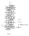
- a host material having a crystal structure of magnetoplumbite type (see Fig. 1) is used.
- the host material contains at least La, and Tb is contained as a luminescence center element.
- the inventors of the present invention have found out that La has the function of converting energy such as vacuum ultraviolet radiation, which is greater than ultraviolet radiation, into energy having a peak wavelength of 350 nm (about 3.5 eV). This function is considered to be due to a CTS (charge transfer state) transition of La.
- the energy of 3.5 eV corresponds to an f-d transition energy of Tb, and therefore, it is considered that La has a sensitizing function in light emission by Tb.
- This CTS transition energy transfer mechanism
- an excitation source is not particularly limited to vacuum ultraviolet radiation, but may be an electron beam, an X-ray or the like having energy of about 7 eV or more.
- Mn is also contained as a luminescence center element.
- the intensity of light emission by Mn depends upon crystal field splitting of the d orbital.
- the inventors have found out that the use of Mn in the host material having the magnetoplumbite-type crystal structure allows emission of green light with high color purity.
- the luminous efficiency of phosphors is affected adversely by trapping of electrons and/or holes and non-radiative attenuation caused by crystal defects in its broad sense and by luminance saturation due to resonance radiation and energy transfer (energy is transferred to adjacent luminescence center elements without light emission) when the luminescence center elements are excited.
- Light emitted by Mn and that emitted by Tb interfere with each other only slightly, and therefore little energy transfers between Mn and Tb. Consequently, a luminance saturation characteristic can be improved as compared with the case where Mn or Tb is used separately.
- the host material is not particularly limited provided that it contains La and has the magnetoplumbite-type crystal structure.
- elements forming the host material Mg, Al, Ca, Sr, Ce, Ba, Zn, Si, Y, B and the like may be mentioned in addition to La.
- the host material may be mixed with other host materials such as CaAl 12 O 19 , SrAl 12 O 19 and the like in an appropriate proportion so as to form a mix crystal.
- the proportion of La in the host material can be reduced, and the use amount of Tb as a luminescence center element can be reduced with reduction of La. Because Tb is an expensive material, the reduction of its use amount will reduce the costs of the green phosphor. Also since the use amount of Mn as a luminescence center element is relatively increased, the green phosphor has excellent color purity.
- Luminescence center elements are not particularly limited provided that at least Tb and Mn are contained.
- Examples of luminescence center elements other than Tb and Mn may include Sc, Ti, V, Cr, Fe, Co, Ni, Cu, Zn, Ga, Ge, Sr, Y, Zr, Nb, Mo, Tc, Ru, Rd, Pd, Ag, Cd, In, Sn, Ba, La, Ce, Pr, Nd, Pm, Sm, Eu, Gd, Dy, Ho, Er, Tm, Yb, Lu, Hf, Ta, W, Tl, Pb, Bi and the like.
- a second green phosphor embodying the present invention has been made from the findings that the CTS transition emission of La has a greater effect in sensitizing Tb than Ce, which has been conventionally used as an element having such sensitizing effect, and therefore the use of La can improve the luminous efficiency.
- CTS means a state in which electrons of elements coordinated around La as a central element are excited and transferred into La.
- the inventors have confirmed that, when excited by vacuum ultraviolet radiation of 147 nm, LaMgAl 11 O 19 :Tb has a luminous efficiency about 20 % higher than CeMgAl 11 O 19 :Tb.
- La 3+ changes to La 2+ in CTS.
- the atomic number of La is 57 and that of Ce is 58, and the difference therebetween is only 2 % or less. Therefore, the f-d transition of La is equivalent to that of Ce.
- La has a sensitizing effect similar to Ce 3+ in light emission by Tb.
- La 2+ cannot excite La 3+ in the ground state and selectively excites Tb to induce light emission.
- Ce 3+ does not excite Tb selectively. Therefore, La 2+ has a stronger Tb sensitizing effect than Ce 3+ .
- the host material is not particularly limited provided that it contains La, does not contain Ce and has the magnetoplumbite-type crystal structure.
- elements forming the host material Mg, Al, Ca, Sr, Ba, Zn, Si, Y, B, Bi and the like may be mentioned in addition to La.
- the host material may be mixed with other host materials such as CaAl 12 O 19 , SrAl 12 O 19 and the like in an appropriate proportion so as to form a mix crystal.
- the proportion of La in the host material can be reduced, and the use amount of Tb as a luminescence center element can be reduced with reduction of La. Because Tb is an expensive material, the reduction of its use amount will reduce the costs of the green phosphor. Also since the use amount of Mn as a luminescence center element is relatively increased, the green phosphor has excellent color purity.
- Luminescence center elements are not particularly limited provided that Tb is contained and Ce is not contained.
- Other luminescence center elements than Tb may be Sc, Ti, V, Cr, Fe, Co, Ni, Cu, Zn, Ga, Ge, Sr, Y, Zr, Nb, Mo, Tc, Ru, Rd, Pd, Ag, Cd, In, Sn, Ba, La, Pr, Nd, Pm, Sm, Eu, Gd, Dy, Ho, Er, Tm, Yb, Lu, Hf, Ta, W, Tl, Pb, Bi and the like.
- (La 1-x Tb x ) (Mg 1-y Mn y ) Al 11 O 19 wherein x is 0.01 to 0.6, y is 0.01 to 0.2 may be mentioned, including (La 0.6 Tb 0.4 )(Mg 0.97 Mn 0.03 )Al 11 O 19 as a particular example
- the composition ratio of La, Mg, and Al may be shifted for improving luminance.
- the above green phosphor may be mix-crystallized with (Ca, Sr)Al 12 O 19 :Mn.
- a host material having the magnetoplumbite type crystal structure (see Fig. 1) is used.
- the host material contains at least La, and Mn and Zn as luminescence center elements.
- the principle that La sensitizes the luminescence center elements are the same as that discussed for the first and second green phosphor.
- a third green phosphor embodying the present invention is based on the findings that the addition of Zn as a luminescence center element improves the light emission amount 10 % or more at the maximum.
- the reason is considered to be that the exciton of Zn is a Wannier exciton whose orbital is not localized around Zn but widely spread in the phosphor. The exciton suppresses non-radiative attenuation of energy caused by defects or impurities in the phosphor, and therefore, the light emission amount increases.
- the host material is not particularly limited provided that it contains La and has the magnetoplumbite-type crystal structure.
- elements forming the host material Mg, Al, Ca, Sr, Ce, Ba, Zn, Si, Y, B and the like may be mentioned in addition to La.
- the host material may be mixed with other host materials such as CaAl 12 O 19 , SrAl 12 O 19 and the like in an appropriate proportion so as to form a mix crystal.
- the proportion of La in the host material can be reduced, and the use amount of the luminescence center elements can be reduced with reduction of La.
- the reduction of the use amount of luminescence center elements will lead to a reduction in the costs of the green phosphor.
- Luminescence center elements are not particularly limited provided that at least Mn and Zn are contained.
- Mn as a luminescent element contributes to obtaining a green phosphor with excellent color purity.
- Examples of luminescence center elements other than Mn and Zn may include Tb, Sc, Ti, V, Cr, Fe, Co, Ni, Cu, Ga, Ge, Sr, Y, Zr, Nb, Mo, Tc, Ru, Rd, Pd, Ag, Cd, In, Sn, Ba, La, Ce, Pr, Nd, Pm, Sm, Eu, Gd, Dy, Ho, Er, Tm, Yb, Lu, Hf, Ta, W, T1, Pb, Bi and the like.
- a third green phosphor embodying the present invention does not contain Ce and/or contains Tb among the above-mentioned luminescence center elements.
- (La 1-x Tb x ) y (Mg 1-a-b Mn a Zn b )Al z O 1.5(x+y)+1 wherein 0 ⁇ x ⁇ 0.5, 0.8 ⁇ y ⁇ 1.2, 0 ⁇ a+b ⁇ 1, 8 ⁇ z ⁇ 30) may be mentioned.
- a preferable range for x is 0.1 to 0.4, a preferable range for a is 0.01 to 0.1, a preferable range for b is 0.1 or less and a more preferable range for b is 0.01 or less.
- the composition ratio of La, Mg and Al may be shifted for improving luminance.
- the above green phosphor may be mix-crystallized with (Ca, Sr)Al 12 O 19 :Mn.
- a phosphor embodying the present invention may be formed by a previously-proposed method. For example, compounds containing La, Tb and/or Mn and compounds containing other elements of the phosphor are weighed in molar ratios appropriate for a desired crystal structure. These compounds are sintered and the obtained sinter of the phosphor is pulverized and classified to give a phosphor having a desired particle size.
- sintering is performed at a sintering temperature of 1,300 to 1,700 °C for 1 to 10 hours in a reducing atmosphere under atmospheric pressure.
- a reaction accelerator composed of a halide such as AlF 2 , MgF 2 , LiF, NaF or the like may be used within a range such that the reaction accelerator does not mar the effect of an embodiment of the present invention.
- the phosphor contains Zn
- Zn may be evaporated if the material for the phosphor is sintered at 900 °C or higher in a reducing atmosphere. Therefore, the material is preferably sintered in a nitrogen atmosphere.
- the sintering temperature is 1,400 °C or lower.
- a phosphor embodying the present invention may be used for luminaires such as fluorescent lamps, display devices such as PDPs, CRTs, fluorescent display tubes and X-ray camera tubes and the like.
- luminaires such as fluorescent lamps
- display devices such as PDPs, CRTs, fluorescent display tubes and X-ray camera tubes and the like.
- phosphors embodying the present invention are applied to a PDP shown in Fig. 2.
- Fig. 2 shows an AC-driven surface discharge PDP with three electrodes.
- An embodiment of the present invention is applicable not only to this type of PDP but also to any type of PDP that has a phosphor.
- a PDP may be not only AC-driven but also DC-driven and may be of reflection type or of transmission type.
- the PDP 100 of Fig. 2 is composed of a front plate and a rear plate.
- the front plate usually includes a plurality of display electrodes formed on a substrate 11, a dielectric layer 17 formed to cover the display electrodes and a protecting layer 18 formed on the dielectric layer 17 and exposed to a discharge space.
- the substrate 11 is not particularly limited and a glass substrate, a quartz glass substrate, a silicon substrate and the like may be mentioned.
- the display electrodes comprise transparent electrodes 41 such as of ITO, and bus electrodes 42 (for example, having a three-layer structure of Cr/Cu/Cr) may be formed on the transparent electrodes 41 for reducing the resistance of the display electrodes.
- the dielectric layer 17 is formed of a material commonly used for PDPs. Particularly, the dielectric layer 17 may be formed by applying a paste of a low-melting glass and a binder onto the substrate, followed by sintering.
- the protecting layer 18 is provided for protecting the dielectric layer 17 from damage due to ion collision caused by discharge for display operation.
- the protecting layer 18 may be formed, for example, of MgO, CaO, SrO, BaO or the like.
- the rear plate usually includes a plurality of address electrodes A formed on a substrate 21 in a direction perpendicular to the display electrodes, a dielectric layer 27 covering the address electrodes A, a plurality of stripe-shaped ribs 29 formed on the dielectric layer 27 between the address electrodes A and phosphor layers 28 formed between the ribs 29 and also covering sidewalls of the ribs.
- the substrate 21 and the dielectric layer 27 may be formed of the same materials as those of the substrate 11 and the dielectric layer 17 of the front plate.
- the address electrode A is formed, for example, of a metal layer of Al, Cr, Cu or the like or a three-layer structure of Cr/Cu/Cr.
- the ribs 29 can be formed by applying a paste of a low-melting glass and a binder onto the dielectric layer 27, followed by drying, and cutting the dried paste by sandblasting. If a photosensitive resin is used as the binder, the ribs 29 can also be formed by exposing and developing the paste using a mask of a desired configuration, followed by sintering.
- the phosphor layers 28 are formed between the ribs 29.
- a phosphor embodying the present invention can be used as a material for the phosphor layers 28.
- a method for forming the phosphor layers 28 is not particularly limited, but may be a previously-proposed method.
- the phosphor layers 28 may be formed by applying a paste of the phosphor dispersed in a solution of a binder in a solvent between the ribs 29 and sintering the paste in the atmosphere.
- the front plate and the rear plate are assembled opposedly to each other with the display-electrodes (41, 42) crossing the address electrodes A and with the display and address electrodes inside, and a discharge gas is fed into a space defined by the ribs 29.
- a discharge gas is fed into a space defined by the ribs 29.
- the phosphor layers are formed on the ribs and the dielectric layer on the rear plate, but phosphor layers may be formed on the protecting film on the front plate in the same manner.
- the molar ratio means the molar ratio of Al, Mg, Mn, La and Tb.
- the resulting mixtures were sintered at 1,500 °C for four hours in a nitrogen atmosphere containing 2 vol% of hydrogen.
- the obtained sinters were pulverized to give phosphors "a” to "c” represented by LaMgAl 11 O 19 :Mn, Tb. It was verified by X-ray diffraction analysis that the resulting phosphors "a” to “c” had the magnetoplumbite-type crystal structure.
- the phosphors "a” to "c” emitted green light upon being irradiated with light of 147 nm wavelength.
- Fig. 3 shows emission spectra of the phosphors by light of 147 nm.
- Fig. 3 shows a change in the emission amount by excitation light of 147 nm and 172 nm with the Mn concentration fixed at 3 atom% and the Tb concentration varied.
- Phosphors "d” and “e” were produced in the same manner as in Example 1 using the following materials.
- the phosphor "d” is represented by LaMgAl 11 O 19 :Mn and the phosphor “e” is , represented by LaMgAl 11 O 19 :Tb.
- the phosphor a is the same as that of Example 1.
- the molar ratio means the molar ratio of Al, Mg, Mn, La and Tb.
- the above phosphors were used for producing surface discharge PDPs with three electrodes in the same manner as in Example 1.
- the phosphors were tested for a change of their luminance with respect to a driving frequency by applying a rectangular pulse having an amplitude of 180 V and a time width of 8 ⁇ s across bus electrodes of display electrodes.
- the results are shown in Fig. 6, in which a dotted line is an ideal line representing a case where the luminance is assumed not to become slower as the driving frequency increases.
- the change of the luminance of the phosphors with respect to the driving frequency was almost equal to that of Zn 2 SiO 4 :Mn. It was found that the phosphor containing both Mn and Tb had an improved luminance saturation characteristic to the driving frequency as compared with those containing either one of Mn and Tb.
- Fig. 7 shows a change of the luminance of the phosphors every time when the PDPs have been operated for given time periods. It was found that the luminance of the phosphors of Example 2 changed less than Zn 2 SiO 4 :Mn.
- Phosphors "f” to “j” represented by LaMgAl 11 O 19 :Tb were produced in the same manner as in Example 1 using the following materials: Materials Phosphor “f” Phosphor “g” Phosphor “h” Phosphor “i” Phosphor “j” Molar Ratio Al 2 O 3 11 11 11 11 MgO 1 1 1 1 1 La 2 O 3 0.95 0.9 0.8 0.7 0.6 Tb 4 O 7 0.05 0.1 0.2 0.3 0.4 AlF 3 0.011 0.011 0.011 0.011 0.011 0.011 0.011 0.011 0.011
- the molar ratio means the molar ratio of Al, Mg, La and Tb.
- the emission amount was almost equal to that of Zn 2 SiO 4 :Mn and larger than that of CeMgAl 11 O 19 :Tb and LaMgAl 11 O 19 :Ce,Tb by 20 to 30 % or more.
- Fig. 9 shows light emission of phosphors "f” to "j” upon irradiation with light of 172 nm wavelength.
- the emission amount was almost equal to or over that of Zn 2 SiO 4 :Mn.
- Fig. 10 shows a change of the emission amount with a change of the concentration of Tb added.
- a PDP was produced using the above phosphors in the same manner as in Example 1.
- a change of luminance with respect to the driving frequency was tested in the same manner as in Example 2 and found to be almost equal to Zn 2 SiO 4 :Mn. Further the phosphors were tested for a change of their luminance every time when the PDPs had been operated for given time periods in the same manner as in Example 2, and it was found that the luminance of the phosphors of Example 3 changed less than Zn2SiO 4 :Mn.
- the molar ratio means the molar ratio of A1, Mg, La, Tb, Mn and Zn.
- the resulting mixtures were sintered at 1400 °C for four hours under nitrogen atmosphere and the obtained sinters were pulverized to give a phosphor "q" represented by LaMgAl 11 O 19 :Mn, Tb, Zn and a phosphor "r” represented by LaZnAl 11 O 19 :Mn. It was confirmed by the X-ray diffraction analysis that the obtained phosphors "q” and "r” had the magnetoplumbite-type crystal structure. The phosphors "q” and "r” emitted green light when they were irradiated with light of 147 nm wavelength.
- Fig. 11 and Fig. 12 illustrate emission spectra by light of 147 nm. The emission amount of the phosphor q was about 105 % of that of Zn 2 SiO 4 :Mn, and the emission peak of the phosphor r was about 1.4 times higher than that of Zn 2 SiO 4 :Mn.
Landscapes
- Chemical & Material Sciences (AREA)
- Inorganic Chemistry (AREA)
- Engineering & Computer Science (AREA)
- Materials Engineering (AREA)
- Organic Chemistry (AREA)
- Luminescent Compositions (AREA)
- Gas-Filled Discharge Tubes (AREA)
Abstract
Description
- The present invention relates to a green phosphor and a device using the same, more particularly to a green phosphor capable of converting received light to light of lower energy (longer wavelength) and a device using the green phosphor. A phosphor embodying the present invention can be suitably used for gas discharge devices such as fluorescent lamps and displays such as plasma display panels (PDPs).
- Phosphors are used in a variety of fields. For example, phosphors are used for luminaires such as fluorescent lamps, displays such as PDPs and X-ray camera tubes.
- Of such phosphors, previously proposed Zn2SiO4:Mn is a green phosphor which is excited by vacuum ultraviolet radiation. This phosphor is advantageous because it has high color purity (chromaticity coordinates: (0.21, 0.72)) and a high luminous efficiency. However, its luminance changes rapidly with time and its life is short. Also, when this phosphor is excited with strong light, the luminous efficiency drops and the luminance is saturated.
- BaAl12O19:Mn, which is a previously-proposed green phosphor, also has high colour purity and high luminous efficiency, but has a short life.
- Previously proposed phosphors having improved life and luminous efficiency are crystals having a magnetoplumbite-type structure with both a rare-earth element and a transition metal added as sensitizers to their luminescence center. Particularly, LaAl11O18:Eu2+, Mn (JJAP, 13(1974) pp.950-956) and SrAl12O19:La, Eu2+, Mn (Philips Technical Review, 37(1977) pp.221-233) are mentioned as examples. With these phosphors, green light can be obtained by first obtaining blue light by exciting Eu2+ using suitable excitation light and exciting Mn2+ using the blue light. The blue light hardly comes outside because most of the blue light is used for exciting Mn2+.
- In addition to the above-mentioned phosphors, SrAl12O19:Mn, Ln (Ln : a trivalent rare-earth element such as Ce3+, Pr3+, Gd3+, Tb3+) has been previously-proposed (USP6,210,605). In this phosphor, energy transfers from the rare-earth element to Mn, and more green light can be obtained than a phosphor in which only Mn contributes to light emission.
- Ce 3+ is well known as a sensitizer element which intensifies light emission from Tb 3+. For example, CeMgAl11O19:Tb is described in J. Luminescence, 9 (1974) pp.415-419 and Philips Technical Review, 37(1977) pp.221-233. In this phosphor, because the energy state of light emitted from Ce is almost equal to the energy state of f-d transition of Tb, energy transfers from Ce to Tb with high efficiency. This phosphor has a long life, but has a lower luminous efficiency than Zn2SiO4:Mn when excited by vacuum ultraviolet radiation. Further, the phosphor has low color purity (chromaticity coordinates: (0.33, 0.61)) because its emission spectrum has sub-peaks at 480 nm (blue, based on transition from 5D4 to 7F4), 580 nm (yellow, based on transition from 5D4 to 7F4) and 600 nm (red, based on transition from 5D4 to 7F3) in addition to a yellowish green emission line at 540 nm as a main peak (based on transition from 5D4 to 7F5). For this reason, this phosphor is not suitable for display devices.
- A phosphor in which Tb is inserted in a borate (YBO3, LuBO3) containing a rare-earth element has a high luminous efficiency, but does not have good color purity, and therefore it is not suitable for display devices.
- Japanese Unexamined Patent Publication No. HEI 5(1993)-86366 discloses a phosphor represented by (Ce1-xTbx) (Mg1-a-bZnaMnb)Al2zO2.5+3z (wherein 0 < x ≦ 0.6, 0 < a+b ≦ 1, 4.5 ≦ z ≦ 15). This phosphor has a spectrum of light emitted from Tb plus light emitted from Mn having a peak wavelength 515 nm. Therefore, the chromaticity is improved as compared with the above-described phosphors. However, regarding the light emission amount upon excitation by vacuum ultraviolet radiation, the phosphor is about 20 % inferior to Zn2SiO4:Mn.
- Accordingly, it is desirable to provide a green phosphor having excellent characteristics such as high color purity, good luminous efficiency, a long life and so on.
- According to an embodiment of a first aspect of the present invention, there is provided a first green phosphor having a magnetoplumbite-type crystal structure and containing at least Mn, La and Tb.
- According to an embodiment of a second aspect of the present invention, there is provided a second green phosphor having a magnetoplumbite-type crystal structure, containing at least Tb and La and not containing Ce.
- According to an embodiment of a third aspect of the present invention, there is provided a third green phosphor having a magnetoplumbite-type crystal structure and containing at least Mn, La and Zn.
- Reference will now be made, by way of example, to the accompanying drawings, in which:
- Fig. 1 is a schematic view of the crystal structure of a green phosphor embodying the present invention;
- Fig. 2 is a schematic perspective view of a PDP;
- Fig. 3 illustrates emission spectra of phosphors in accordance with Example 1 of the present invention;
- Fig. 4 illustrates emission spectra of phosphors of LAM:Tb in accordance with Example 1 of the present invention;
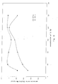
- Fig. 5 is a graph showing a dependence of the emission amount of LAM:Tb of Example 1 upon the concentration of Tb;
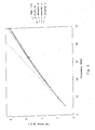
- Fig. 6 is a graph showing a dependence of the luminance of phosphors of Example 2 upon driving frequency;
- Fig. 7 is a graph showing a change of the luminance of phosphors of Example 2 at every drive period of time;
- Fig. 8 illustrates emission spectra of phosphors in accordance with Example 3 of the present invention;
- Fig. 9 illustrates emission spectra of phosphors of LAM:Mn,Tb in accordance with Example 3 of the present invention;
- Fig. 10 is a graph showing a dependence of the luminance of phosphors of LAM:Mn,Tb of Example 3 upon the concentration of Tb;
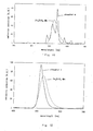
- Fig. 11 illustrates an emission spectrum of a phosphor q in accordance with Example 4 of the present invention; and
- Fig. 12 illustrates an emission spectrum of a phosphor r in accordance with Example 4 of the present invention.
-
- In a first green phosphor embodying the present invention, a host material having a crystal structure of magnetoplumbite type (see Fig. 1) is used. The host material contains at least La, and Tb is contained as a luminescence center element. The inventors of the present invention have found out that La has the function of converting energy such as vacuum ultraviolet radiation, which is greater than ultraviolet radiation, into energy having a peak wavelength of 350 nm (about 3.5 eV). This function is considered to be due to a CTS (charge transfer state) transition of La. The energy of 3.5 eV corresponds to an f-d transition energy of Tb, and therefore, it is considered that La has a sensitizing function in light emission by Tb. This CTS transition (energy transfer mechanism) takes place at about 7 eV or more. For this reason, an excitation source is not particularly limited to vacuum ultraviolet radiation, but may be an electron beam, an X-ray or the like having energy of about 7 eV or more.
- In a first green phosphor embodying the present invention, Mn is also contained as a luminescence center element. The intensity of light emission by Mn depends upon crystal field splitting of the d orbital. However, the inventors have found out that the use of Mn in the host material having the magnetoplumbite-type crystal structure allows emission of green light with high color purity. The luminous efficiency of phosphors is affected adversely by trapping of electrons and/or holes and non-radiative attenuation caused by crystal defects in its broad sense and by luminance saturation due to resonance radiation and energy transfer (energy is transferred to adjacent luminescence center elements without light emission) when the luminescence center elements are excited. Light emitted by Mn and that emitted by Tb interfere with each other only slightly, and therefore little energy transfers between Mn and Tb. Consequently, a luminance saturation characteristic can be improved as compared with the case where Mn or Tb is used separately.
- Further, it has also been found out that, when Mn and Tb are used together, phosphorescence can be suppressed as compared with the case where Mn is used alone. This suppression gives a great advantage to display devices such as PDPs.
- The following are examples of a first green phosphor embodying the present invention:
- First, the host material is not particularly limited provided that it contains La and has the magnetoplumbite-type crystal structure. As elements forming the host material, Mg, Al, Ca, Sr, Ce, Ba, Zn, Si, Y, B and the like may be mentioned in addition to La. More particularly, the host material may be LaMgAl11O19, LaxAlyOz (x : y : z = 0.5 to 1.2 : 11 to 12 : 18 to 19.5) or the like. Further the host material may be mixed with other host materials such as CaAl12O19, SrAl12O19 and the like in an appropriate proportion so as to form a mix crystal. By mix-crystallization, the proportion of La in the host material can be reduced, and the use amount of Tb as a luminescence center element can be reduced with reduction of La. Because Tb is an expensive material, the reduction of its use amount will reduce the costs of the green phosphor. Also since the use amount of Mn as a luminescence center element is relatively increased, the green phosphor has excellent color purity.
- Luminescence center elements are not particularly limited provided that at least Tb and Mn are contained. Examples of luminescence center elements other than Tb and Mn may include Sc, Ti, V, Cr, Fe, Co, Ni, Cu, Zn, Ga, Ge, Sr, Y, Zr, Nb, Mo, Tc, Ru, Rd, Pd, Ag, Cd, In, Sn, Ba, La, Ce, Pr, Nd, Pm, Sm, Eu, Gd, Dy, Ho, Er, Tm, Yb, Lu, Hf, Ta, W, Tl, Pb, Bi and the like.
- A second green phosphor embodying the present invention has been made from the findings that the CTS transition emission of La has a greater effect in sensitizing Tb than Ce, which has been conventionally used as an element having such sensitizing effect, and therefore the use of La can improve the luminous efficiency. CTS means a state in which electrons of elements coordinated around La as a central element are excited and transferred into La. The inventors have confirmed that, when excited by vacuum ultraviolet radiation of 147 nm, LaMgAl11O19:Tb has a luminous efficiency about 20 % higher than CeMgAl11O19:Tb.
- In detail, La3+ changes to La2+ in CTS. One electron exists in the f orbital of La2+ as in Ce3+. The atomic number of La is 57 and that of Ce is 58, and the difference therebetween is only 2 % or less. Therefore, the f-d transition of La is equivalent to that of Ce. Thus La has a sensitizing effect similar to Ce3+ in light emission by Tb. Usually La2+ cannot excite La3+ in the ground state and selectively excites Tb to induce light emission. However, Ce3+ does not excite Tb selectively. Therefore, La2+ has a stronger Tb sensitizing effect than Ce3+.
- The following are examples of a second green phosphor embodying the present invention:
- First, the host material is not particularly limited provided that it contains La, does not contain Ce and has the magnetoplumbite-type crystal structure. As elements forming the host material, Mg, Al, Ca, Sr, Ba, Zn, Si, Y, B, Bi and the like may be mentioned in addition to La. Particularly, the host material may be LaMgAl11O19, LaxAlyOz (x : y : z = 0.5 to 1.2 : 11 to 12 : 18 to 19.5) or the like. Further the host material may be mixed with other host materials such as CaAl12O19, SrAl12O19 and the like in an appropriate proportion so as to form a mix crystal. By mix-crystallization, the proportion of La in the host material can be reduced, and the use amount of Tb as a luminescence center element can be reduced with reduction of La. Because Tb is an expensive material, the reduction of its use amount will reduce the costs of the green phosphor. Also since the use amount of Mn as a luminescence center element is relatively increased, the green phosphor has excellent color purity.
- Luminescence center elements are not particularly limited provided that Tb is contained and Ce is not contained. Other luminescence center elements than Tb may be Sc, Ti, V, Cr, Fe, Co, Ni, Cu, Zn, Ga, Ge, Sr, Y, Zr, Nb, Mo, Tc, Ru, Rd, Pd, Ag, Cd, In, Sn, Ba, La, Pr, Nd, Pm, Sm, Eu, Gd, Dy, Ho, Er, Tm, Yb, Lu, Hf, Ta, W, Tl, Pb, Bi and the like.
- As a green phosphor satisfying the conditions required of first and second green phosphors embodying the present invention, (La1-xTbx) (Mg1-yMny) Al11O19 wherein x is 0.01 to 0.6, y is 0.01 to 0.2 may be mentioned, including (La0.6Tb0.4)(Mg0.97Mn0.03)Al11O19 as a particular example Also as a generally known technique regarding phosphors, the composition ratio of La, Mg, and Al may be shifted for improving luminance.
- Further; the above green phosphor may be mix-crystallized with (Ca, Sr)Al12O19:Mn.
- In a third green phosphor embodying the present invention, a host material having the magnetoplumbite type crystal structure (see Fig. 1) is used. The host material contains at least La, and Mn and Zn as luminescence center elements. The principle that La sensitizes the luminescence center elements are the same as that discussed for the first and second green phosphor.
- Further, a third green phosphor embodying the present invention is based on the findings that the addition of Zn as a luminescence center element improves the
light emission amount 10 % or more at the maximum. The reason is considered to be that the exciton of Zn is a Wannier exciton whose orbital is not localized around Zn but widely spread in the phosphor. The exciton suppresses non-radiative attenuation of energy caused by defects or impurities in the phosphor, and therefore, the light emission amount increases. - The following are examples of a third green phosphor embodying the present invention:
- First, the host material is not particularly limited provided that it contains La and has the magnetoplumbite-type crystal structure. As elements forming the host material, Mg, Al, Ca, Sr, Ce, Ba, Zn, Si, Y, B and the like may be mentioned in addition to La. Particularly, the host material may be LaMgAl11O19, LaxAlyOz (x : y : z = 0.5 to 1.2 : 11 to 12 : 18 to 19.5) or the like. Further the host material may be mixed with other host materials such as CaAl12O19, SrAl12O19 and the like in an appropriate proportion so as to form a mix crystal. By mix-crystallization, the proportion of La in the host material can be reduced, and the use amount of the luminescence center elements can be reduced with reduction of La. The reduction of the use amount of luminescence center elements will lead to a reduction in the costs of the green phosphor.
- Luminescence center elements are not particularly limited provided that at least Mn and Zn are contained. The use of Mn as a luminescent element contributes to obtaining a green phosphor with excellent color purity. Examples of luminescence center elements other than Mn and Zn may include Tb, Sc, Ti, V, Cr, Fe, Co, Ni, Cu, Ga, Ge, Sr, Y, Zr, Nb, Mo, Tc, Ru, Rd, Pd, Ag, Cd, In, Sn, Ba, La, Ce, Pr, Nd, Pm, Sm, Eu, Gd, Dy, Ho, Er, Tm, Yb, Lu, Hf, Ta, W, T1, Pb, Bi and the like.
- Preferably, a third green phosphor embodying the present invention does not contain Ce and/or contains Tb among the above-mentioned luminescence center elements.
- As a green phosphor satisfying the conditions required of a third green phosphor embodying the present invention, (La1-xTbx)y(Mg1-a-bMnaZnb)AlzO1.5(x+y)+1 wherein 0≦x≦0.5, 0.8≦y≦ 1.2, 0<a+b≦1, 8≦z≦30) may be mentioned. A preferable range for x is 0.1 to 0.4, a preferable range for a is 0.01 to 0.1, a preferable range for b is 0.1 or less and a more preferable range for b is 0.01 or less. Also as a generally known technique regarding phosphors, the composition ratio of La, Mg and Al may be shifted for improving luminance.
- Further, the above green phosphor may be mix-crystallized with (Ca, Sr)Al12O19:Mn.
- A phosphor embodying the present invention may be formed by a previously-proposed method. For example, compounds containing La, Tb and/or Mn and compounds containing other elements of the phosphor are weighed in molar ratios appropriate for a desired crystal structure. These compounds are sintered and the obtained sinter of the phosphor is pulverized and classified to give a phosphor having a desired particle size.
- Particularly, sintering is performed at a sintering temperature of 1,300 to 1,700 °C for 1 to 10 hours in a reducing atmosphere under atmospheric pressure. For the purpose of reducing the sintering temperature, a reaction accelerator composed of a halide such as AlF2, MgF2, LiF, NaF or the like may be used within a range such that the reaction accelerator does not mar the effect of an embodiment of the present invention.
- In the case where the phosphor contains Zn, Zn may be evaporated if the material for the phosphor is sintered at 900 °C or higher in a reducing atmosphere. Therefore, the material is preferably sintered in a nitrogen atmosphere. For preventing Zn from evaporating, it is preferable that the sintering temperature is 1,400 °C or lower.
- A phosphor embodying the present invention may be used for luminaires such as fluorescent lamps, display devices such as PDPs, CRTs, fluorescent display tubes and X-ray camera tubes and the like. In the following examples, phosphors embodying the present invention are applied to a PDP shown in Fig. 2.
- Fig. 2 shows an AC-driven surface discharge PDP with three electrodes. An embodiment of the present invention is applicable not only to this type of PDP but also to any type of PDP that has a phosphor. For example, a PDP may be not only AC-driven but also DC-driven and may be of reflection type or of transmission type.
- The
PDP 100 of Fig. 2 is composed of a front plate and a rear plate. - First, the front plate usually includes a plurality of display electrodes formed on a substrate 11, a dielectric layer 17 formed to cover the display electrodes and a protecting
layer 18 formed on the dielectric layer 17 and exposed to a discharge space. - The substrate 11 is not particularly limited and a glass substrate, a quartz glass substrate, a silicon substrate and the like may be mentioned.
- The display electrodes comprise
transparent electrodes 41 such as of ITO, and bus electrodes 42 (for example, having a three-layer structure of Cr/Cu/Cr) may be formed on thetransparent electrodes 41 for reducing the resistance of the display electrodes. - The dielectric layer 17 is formed of a material commonly used for PDPs. Particularly, the dielectric layer 17 may be formed by applying a paste of a low-melting glass and a binder onto the substrate, followed by sintering.
- The protecting
layer 18 is provided for protecting the dielectric layer 17 from damage due to ion collision caused by discharge for display operation. The protectinglayer 18 may be formed, for example, of MgO, CaO, SrO, BaO or the like. - Next, the rear plate usually includes a plurality of address electrodes A formed on a
substrate 21 in a direction perpendicular to the display electrodes, adielectric layer 27 covering the address electrodes A, a plurality of stripe-shapedribs 29 formed on thedielectric layer 27 between the address electrodes A and phosphor layers 28 formed between theribs 29 and also covering sidewalls of the ribs. - The
substrate 21 and thedielectric layer 27 may be formed of the same materials as those of the substrate 11 and the dielectric layer 17 of the front plate. - The address electrode A is formed, for example, of a metal layer of Al, Cr, Cu or the like or a three-layer structure of Cr/Cu/Cr.
- The
ribs 29 can be formed by applying a paste of a low-melting glass and a binder onto thedielectric layer 27, followed by drying, and cutting the dried paste by sandblasting. If a photosensitive resin is used as the binder, theribs 29 can also be formed by exposing and developing the paste using a mask of a desired configuration, followed by sintering. - Referring to Fig. 2, the phosphor layers 28 are formed between the
ribs 29. A phosphor embodying the present invention can be used as a material for the phosphor layers 28. A method for forming the phosphor layers 28 is not particularly limited, but may be a previously-proposed method. For example, the phosphor layers 28 may be formed by applying a paste of the phosphor dispersed in a solution of a binder in a solvent between theribs 29 and sintering the paste in the atmosphere. - Next, the front plate and the rear plate are assembled opposedly to each other with the display-electrodes (41, 42) crossing the address electrodes A and with the display and address electrodes inside, and a discharge gas is fed into a space defined by the
ribs 29. Thus thePDP 100 is produced. - In the above-described PDP, among the ribs, the dielectric layer and the protecting layer which define the discharge space, the phosphor layers are formed on the ribs and the dielectric layer on the rear plate, but phosphor layers may be formed on the protecting film on the front plate in the same manner.
- Embodiments of the present invention are explained in further details by way of the following examples, but the present invention should not be construed to be limited to these examples.
- Materials, with a suitable amount of ethanol added thereto, were mixed for three hours under the following conditions:
Materials Phosphor "a" Phosphor "b" Phosphor "c" Molar Ratio Al2O3 11 11 11 MgO 0.97 0.97 0.97 MnO 0.03 0.03 0.03 La2O3 0.8 0.7 0.6 Tb4O7 0.2 0.3 0.4 AlF3 0.011 0.011 0.011 - In the table, the molar ratio means the molar ratio of Al, Mg, Mn, La and Tb.
- The resulting mixtures were sintered at 1,500 °C for four hours in a nitrogen atmosphere containing 2 vol% of hydrogen. The obtained sinters were pulverized to give phosphors "a" to "c" represented by LaMgAl11O19:Mn, Tb. It was verified by X-ray diffraction analysis that the resulting phosphors "a" to "c" had the magnetoplumbite-type crystal structure. The phosphors "a" to "c" emitted green light upon being irradiated with light of 147 nm wavelength. Fig. 3 shows emission spectra of the phosphors by light of 147 nm. The amount and chromaticity of the light emitted from the phosphors were almost equal to those of Zn2SiO4:Mn. In Fig. 3, the host material is referred to LAM for short. Light emission by light of 172 nm is also shown (see Fig. 4). In this case, an emission amount about 1.3 times larger than the maximum emission amount of Zn2SiO4:Mn can be obtained. Further, Fig. 5 shows a change in the emission amount by excitation light of 147 nm and 172 nm with the Mn concentration fixed at 3 atom% and the Tb concentration varied.
-
- Display electrodes
- Transparent electrode width: 280 µm
- Bus electrode width: 100 µm
- Discharge gap between display electrodes: 100 µm
- Thickness of dielectric layer: 30 µm
- Height of ribs: 100 µm
- Pitch of ribs: 360 µm
- Discharge gas of Ne-Xe (5 %)
- Gas pressure: 500 Torr
-
- Phosphors "d" and "e" were produced in the same manner as in Example 1 using the following materials. The phosphor "d" is represented by LaMgAl11O19:Mn and the phosphor "e" is , represented by LaMgAl11O19:Tb. The phosphor a is the same as that of Example 1.
Materials Phosphor "d" Phosphor "e" Phosphor "a" Molar Ratio Al2O3 11 11 11 MgO 0.97 1 0.97 MnO 0.03 - 0.03 La2O3 1 0.6 0.6 Tb4O7 - 0.4 0.4 AlF3 0.011 0.011 0.011 - In the table, the molar ratio means the molar ratio of Al, Mg, Mn, La and Tb.
- The above phosphors were used for producing surface discharge PDPs with three electrodes in the same manner as in Example 1. The phosphors were tested for a change of their luminance with respect to a driving frequency by applying a rectangular pulse having an amplitude of 180 V and a time width of 8 µs across bus electrodes of display electrodes. The results are shown in Fig. 6, in which a dotted line is an ideal line representing a case where the luminance is assumed not to become slower as the driving frequency increases.
- The change of the luminance of the phosphors with respect to the driving frequency was almost equal to that of Zn2SiO4:Mn. It was found that the phosphor containing both Mn and Tb had an improved luminance saturation characteristic to the driving frequency as compared with those containing either one of Mn and Tb.
- Fig. 7 shows a change of the luminance of the phosphors every time when the PDPs have been operated for given time periods. It was found that the luminance of the phosphors of Example 2 changed less than Zn2SiO4:Mn.
- Phosphors "f" to "j" represented by LaMgAl11O19:Tb were produced in the same manner as in Example 1 using the following materials:
Materials Phosphor "f" Phosphor "g" Phosphor "h" Phosphor "i" Phosphor "j" Molar Ratio Al2O3 11 11 11 11 11 MgO 1 1 1 1 1 La2O3 0.95 0.9 0.8 0.7 0.6 Tb4O7 0.05 0.1 0.2 0.3 0.4 AlF3 0.011 0.011 0.011 0.011 0.011 - In the table, the molar ratio means the molar ratio of Al, Mg, La and Tb.
- The obtained phosphors "f" to "j" emitted green light upon being irradiated with light of 147 nm wavelength as shown in Fig. 8. The emission amount was almost equal to that of Zn2SiO4:Mn and larger than that of CeMgAl11O19:Tb and LaMgAl11O19:Ce,Tb by 20 to 30 % or more. Fig. 9 shows light emission of phosphors "f" to "j" upon irradiation with light of 172 nm wavelength. The emission amount was almost equal to or over that of Zn2SiO4:Mn. Fig. 10 shows a change of the emission amount with a change of the concentration of Tb added.
- A PDP was produced using the above phosphors in the same manner as in Example 1. A change of luminance with respect to the driving frequency was tested in the same manner as in Example 2 and found to be almost equal to Zn2SiO4:Mn. Further the phosphors were tested for a change of their luminance every time when the PDPs had been operated for given time periods in the same manner as in Example 2, and it was found that the luminance of the phosphors of Example 3 changed less than Zn2SiO4:Mn.
- Materials, with a suitable amount of ethanol added thereto, were mixed for three hours under the following conditions:
Materials Phosphor "q" Phosphor "r" Molar Ratio Al2O3 11 11 MgO 0.967 0 La2O3 0.7 1 Tb2O3 0.3 0 MnCO3 0.03 0.05 ZnO 0.003 0.95 MgF2 0.03 0.03 - In the table, the molar ratio means the molar ratio of A1, Mg, La, Tb, Mn and Zn.
- The resulting mixtures were sintered at 1400 °C for four hours under nitrogen atmosphere and the obtained sinters were pulverized to give a phosphor "q" represented by LaMgAl11O19:Mn, Tb, Zn and a phosphor "r" represented by LaZnAl11O19:Mn. It was confirmed by the X-ray diffraction analysis that the obtained phosphors "q" and "r" had the magnetoplumbite-type crystal structure. The phosphors "q" and "r" emitted green light when they were irradiated with light of 147 nm wavelength. Fig. 11 and Fig. 12 illustrate emission spectra by light of 147 nm. The emission amount of the phosphor q was about 105 % of that of Zn2SiO4:Mn, and the emission peak of the phosphor r was about 1.4 times higher than that of Zn2SiO4:Mn.
Claims (10)
- A green phosphor having a magnetoplumbite-type crystal structure, which contains at least Mn, La and Tb.
- A green phosphor according to claim 1, which comprises LaMgAl11O19:Mn, Tb.
- A green phosphor having a magnetoplumbite-type crystal structure, which contains at least Tb and La but does not contain Ce.
- A green phosphor according to claim 3, which comprises LaMgAl11O19:Tb or LaMgAl11O19:Mn, Tb.
- A green phosphor having a magnetoplumbite-type crystal structure, which contains at least Mn, La and Zn.
- A green phosphor according to claim 5, which does not contain Ce and/or which contains Tb.
- A green phosphor according to claim 6, which is represented by the formula:
- A green phosphor according to any one of claims 1 to 7, which is capable of being excited by vacuum ultraviolet radiation.
- A gas discharge device using a green phosphor as set forth in any one of claims 1 to 8.
- A display device using a green phosphor as set forth in any one of claims 1 to 8.
Applications Claiming Priority (4)
| Application Number | Priority Date | Filing Date | Title |
|---|---|---|---|
| JP2002074423 | 2002-03-18 | ||
| JP2002074423 | 2002-03-18 | ||
| JP2003028846 | 2003-02-05 | ||
| JP2003028846A JP4235748B2 (en) | 2002-03-18 | 2003-02-05 | Display device |
Publications (2)
| Publication Number | Publication Date |
|---|---|
| EP1359205A1 true EP1359205A1 (en) | 2003-11-05 |
| EP1359205B1 EP1359205B1 (en) | 2005-06-01 |
Family
ID=28043753
Family Applications (1)
| Application Number | Title | Priority Date | Filing Date |
|---|---|---|---|
| EP03251651A Expired - Lifetime EP1359205B1 (en) | 2002-03-18 | 2003-03-18 | Green phosphor and device using the same |
Country Status (7)
| Country | Link |
|---|---|
| US (1) | US7037445B2 (en) |
| EP (1) | EP1359205B1 (en) |
| JP (1) | JP4235748B2 (en) |
| KR (1) | KR100910442B1 (en) |
| CN (1) | CN1249197C (en) |
| DE (1) | DE60300743T2 (en) |
| TW (1) | TWI282812B (en) |
Cited By (3)
| Publication number | Priority date | Publication date | Assignee | Title |
|---|---|---|---|---|
| US7025902B2 (en) | 2004-03-02 | 2006-04-11 | Matsushita Electric Industrial Co., Ltd. | Green emitting phosphor material and plasma display panel using the same |
| US7410599B2 (en) | 2005-03-01 | 2008-08-12 | Matsushita Electric Industrial Co., Ltd | Stable green phosphor and plasma display panel using the same |
| CN101906300A (en) * | 2010-08-16 | 2010-12-08 | 江门市科恒实业股份有限公司 | Cerium-gadolinium-manganese coactivated green rare earth luminescent material and preparation method thereof |
Families Citing this family (19)
| Publication number | Priority date | Publication date | Assignee | Title |
|---|---|---|---|---|
| CN100383217C (en) * | 2002-10-31 | 2008-04-23 | 住友化学工业株式会社 | Phosphors for Vacuum Ultraviolet Excitation Light-Emitting Elements |
| JP4415578B2 (en) * | 2003-06-30 | 2010-02-17 | パナソニック株式会社 | Plasma display device |
| JP4244727B2 (en) * | 2003-06-30 | 2009-03-25 | パナソニック株式会社 | Plasma display device |
| KR100651277B1 (en) * | 2003-07-25 | 2006-11-28 | 엘지전자 주식회사 | Green phosphor and plasma display panel |
| KR100553216B1 (en) * | 2003-12-23 | 2006-02-22 | 주식회사 엘지화학 | Novel Blue Phosphors and Manufacturing Methods Thereof |
| US7528537B2 (en) | 2003-12-25 | 2009-05-05 | Sumitomo Chemical Company, Limited | Phosphor, phosphor paste, and vacuum ultraviolet excited light-emitting device |
| KR100589404B1 (en) * | 2004-01-26 | 2006-06-14 | 삼성에스디아이 주식회사 | Green phosphor for plasma display panel and plasma display panel comprising same |
| KR20060012778A (en) * | 2004-08-04 | 2006-02-09 | 삼성코닝 주식회사 | Phosphor, fluorescent lamp and plasma display panel including the same |
| JP4507862B2 (en) * | 2004-12-01 | 2010-07-21 | 株式会社日立プラズマパテントライセンシング | Phosphor and apparatus using the same |
| TWI319777B (en) | 2005-03-30 | 2010-01-21 | Lamp having good maintenance behavior of brightness and color coordinations | |
| JP4532329B2 (en) | 2005-04-12 | 2010-08-25 | パナソニック株式会社 | Plasma display panel |
| JP4825499B2 (en) * | 2005-11-18 | 2011-11-30 | 日立プラズマディスプレイ株式会社 | Phosphors for plasma display panels |
| WO2007080649A1 (en) * | 2006-01-13 | 2007-07-19 | Hitachi Plasma Display Limited | Green fluorophor and plasma display panel |
| KR100945252B1 (en) * | 2007-10-16 | 2010-03-03 | 한국과학기술원 | Green light-emitting phosphor, method for manufacturing the same and fluorescent lamp comprising the same |
| JP5580865B2 (en) * | 2012-10-23 | 2014-08-27 | 浜松ホトニクス株式会社 | Ultraviolet light generation target, electron beam excited ultraviolet light source, and method for producing ultraviolet light generation target |
| JP6029926B2 (en) * | 2012-10-23 | 2016-11-24 | 浜松ホトニクス株式会社 | Ultraviolet light generation target, electron beam excited ultraviolet light source, and method for producing ultraviolet light generation target |
| JP5580866B2 (en) * | 2012-10-23 | 2014-08-27 | 浜松ホトニクス株式会社 | Ultraviolet light generation target, electron beam excited ultraviolet light source, and method for producing ultraviolet light generation target |
| CN102942923A (en) * | 2012-11-21 | 2013-02-27 | 宜兴新威集团有限公司 | Green phosphor and preparation method thereof |
| CN105130415B (en) * | 2015-08-14 | 2016-12-14 | 东台市圣德尔耐热材料有限公司 | Ln1 xsrxmg1 ymnyal11 ztizo19nano ceramics heat barrier coat material and preparation method thereof |
Citations (4)
| Publication number | Priority date | Publication date | Assignee | Title |
|---|---|---|---|---|
| GB1393040A (en) * | 1972-12-09 | 1975-05-07 | Philips Electronic Associated | Luminescent materials |
| US4150321A (en) * | 1977-01-19 | 1979-04-17 | U.S. Philips Corporation | Luminescent aluminates and mercury vapor discharge lamp containing the same |
| US5518808A (en) * | 1992-12-18 | 1996-05-21 | E. I. Du Pont De Nemours And Company | Luminescent materials prepared by coating luminescent compositions onto substrate particles |
| US6222312B1 (en) * | 2000-03-17 | 2001-04-24 | Philips Electronics North America Corp. | Fluorescent lamp having wide bandwidth blue-green phosphor |
Family Cites Families (6)
| Publication number | Priority date | Publication date | Assignee | Title |
|---|---|---|---|---|
| NL160869C (en) * | 1972-11-03 | Philips Nv | LUMINESCENT SCREEN, AS WELL AS DISCHARGE LAMP AND KATHODE BEAM TUBE, FITTED WITH SUCH SCREEN. | |
| US4081398A (en) * | 1975-06-30 | 1978-03-28 | Dai Nippon Toryo Co., Ltd. | Fluorescent compositions |
| FR2486519A1 (en) * | 1980-07-08 | 1982-01-15 | Centre Nat Rech Scient | MIXED ALUMINUM OXIDES, PROCESS FOR THEIR PRODUCTION AND THEIR APPLICATION |
| JP2894654B2 (en) | 1991-09-26 | 1999-05-24 | 松下電子工業株式会社 | Aluminate phosphor and fluorescent lamp using the same |
| KR100294506B1 (en) * | 1999-06-30 | 2001-07-03 | 김순택 | Green emitting phosphor compositions and projection type cathod-ray tube having phosphor layer manufactured using the same |
| US6210605B1 (en) * | 1999-07-26 | 2001-04-03 | General Electric Company | Mn2+ activated green emitting SrAL12O19 luminiscent material |
-
2003
- 2003-02-05 JP JP2003028846A patent/JP4235748B2/en not_active Expired - Fee Related
- 2003-03-08 KR KR1020030014581A patent/KR100910442B1/en not_active Expired - Fee Related
- 2003-03-13 US US10/386,664 patent/US7037445B2/en not_active Expired - Fee Related
- 2003-03-17 TW TW092105823A patent/TWI282812B/en active
- 2003-03-18 DE DE60300743T patent/DE60300743T2/en not_active Expired - Fee Related
- 2003-03-18 CN CNB031072348A patent/CN1249197C/en not_active Expired - Fee Related
- 2003-03-18 EP EP03251651A patent/EP1359205B1/en not_active Expired - Lifetime
Patent Citations (4)
| Publication number | Priority date | Publication date | Assignee | Title |
|---|---|---|---|---|
| GB1393040A (en) * | 1972-12-09 | 1975-05-07 | Philips Electronic Associated | Luminescent materials |
| US4150321A (en) * | 1977-01-19 | 1979-04-17 | U.S. Philips Corporation | Luminescent aluminates and mercury vapor discharge lamp containing the same |
| US5518808A (en) * | 1992-12-18 | 1996-05-21 | E. I. Du Pont De Nemours And Company | Luminescent materials prepared by coating luminescent compositions onto substrate particles |
| US6222312B1 (en) * | 2000-03-17 | 2001-04-24 | Philips Electronics North America Corp. | Fluorescent lamp having wide bandwidth blue-green phosphor |
Non-Patent Citations (1)
| Title |
|---|
| CINIBULK M K M K: "Hexaluminates as a cleavable fiber-matrix interphase: synthesis, texture development, and phase compatibility", JOURNAL OF THE EUROPEAN CERAMIC SOCIETY, ELSEVIER SCIENCE PUBLISHERS, BARKING, ESSEX, GB, vol. 20, no. 5, May 2000 (2000-05-01), pages 569 - 582, XP004193035, ISSN: 0955-2219 * |
Cited By (4)
| Publication number | Priority date | Publication date | Assignee | Title |
|---|---|---|---|---|
| US7025902B2 (en) | 2004-03-02 | 2006-04-11 | Matsushita Electric Industrial Co., Ltd. | Green emitting phosphor material and plasma display panel using the same |
| US7410599B2 (en) | 2005-03-01 | 2008-08-12 | Matsushita Electric Industrial Co., Ltd | Stable green phosphor and plasma display panel using the same |
| CN101906300A (en) * | 2010-08-16 | 2010-12-08 | 江门市科恒实业股份有限公司 | Cerium-gadolinium-manganese coactivated green rare earth luminescent material and preparation method thereof |
| CN101906300B (en) * | 2010-08-16 | 2013-09-18 | 江门市科恒实业股份有限公司 | Cerium-gadolinium-manganese coactivated green rare earth luminescent material and preparation method thereof |
Also Published As
| Publication number | Publication date |
|---|---|
| DE60300743T2 (en) | 2005-10-27 |
| US20030173542A1 (en) | 2003-09-18 |
| US7037445B2 (en) | 2006-05-02 |
| KR20030076281A (en) | 2003-09-26 |
| JP2003342566A (en) | 2003-12-03 |
| CN1249197C (en) | 2006-04-05 |
| KR100910442B1 (en) | 2009-08-04 |
| CN1445333A (en) | 2003-10-01 |
| JP4235748B2 (en) | 2009-03-11 |
| EP1359205B1 (en) | 2005-06-01 |
| DE60300743D1 (en) | 2005-07-07 |
| TWI282812B (en) | 2007-06-21 |
| TW200305634A (en) | 2003-11-01 |
Similar Documents
| Publication | Publication Date | Title |
|---|---|---|
| EP1359205B1 (en) | Green phosphor and device using the same | |
| KR100858269B1 (en) | Method of producing aluminate fluorescent substance, a fluorescent substance and a device containing a fluorescent substance | |
| US20060017385A1 (en) | Plasma display | |
| CN100366705C (en) | Phosphor and devices using it | |
| US20060017384A1 (en) | Plasma display | |
| JP3947175B2 (en) | Plasma display panel | |
| US6861797B1 (en) | green phosphor and device using the same | |
| US8114312B2 (en) | Display device and green phosphor | |
| US20030057832A1 (en) | Plasma picture screen with increased efficiency | |
| CN101142295A (en) | Display device and green phosphor | |
| JP4870690B2 (en) | Green phosphor and plasma display panel | |
| JP3861125B2 (en) | Plasma display panel comprising La / Al / Mg composite oxide phosphor | |
| US20060145591A1 (en) | Green light emitting phosphor for low voltage/high current density and field emission type display including the same | |
| KR100890100B1 (en) | Display device and green phosphor | |
| US20020160226A1 (en) | Plasma picture screen with a phosphor layer | |
| CN101133136A (en) | Display device and green phosphor | |
| LAYER | co), United States c) Patent Application Publication do Pub. No.: US 2001/0024088A1 | |
| JP2006274152A (en) | Display device, phosphor and manufacturing method thereof | |
| JP2005089692A (en) | Green phosphor and apparatus using the same |
Legal Events
| Date | Code | Title | Description |
|---|---|---|---|
| PUAI | Public reference made under article 153(3) epc to a published international application that has entered the european phase |
Free format text: ORIGINAL CODE: 0009012 |
|
| AK | Designated contracting states |
Kind code of ref document: A1 Designated state(s): AT BE BG CH CY CZ DE DK EE ES FI FR GB GR HU IE IT LI LU MC NL PT RO SE SI SK TR |
|
| AX | Request for extension of the european patent |
Extension state: AL LT LV MK RO |
|
| 17P | Request for examination filed |
Effective date: 20031008 |
|
| AKX | Designation fees paid |
Designated state(s): DE FR GB |
|
| GRAP | Despatch of communication of intention to grant a patent |
Free format text: ORIGINAL CODE: EPIDOSNIGR1 |
|
| GRAS | Grant fee paid |
Free format text: ORIGINAL CODE: EPIDOSNIGR3 |
|
| GRAA | (expected) grant |
Free format text: ORIGINAL CODE: 0009210 |
|
| AK | Designated contracting states |
Kind code of ref document: B1 Designated state(s): DE FR GB |
|
| REG | Reference to a national code |
Ref country code: GB Ref legal event code: FG4D |
|
| REF | Corresponds to: |
Ref document number: 60300743 Country of ref document: DE Date of ref document: 20050707 Kind code of ref document: P |
|
| REG | Reference to a national code |
Ref country code: GB Ref legal event code: 732E |
|
| ET | Fr: translation filed | ||
| PLBE | No opposition filed within time limit |
Free format text: ORIGINAL CODE: 0009261 |
|
| STAA | Information on the status of an ep patent application or granted ep patent |
Free format text: STATUS: NO OPPOSITION FILED WITHIN TIME LIMIT |
|
| REG | Reference to a national code |
Ref country code: FR Ref legal event code: TP |
|
| 26N | No opposition filed |
Effective date: 20060302 |
|
| REG | Reference to a national code |
Ref country code: GB Ref legal event code: 732E |
|
| REG | Reference to a national code |
Ref country code: FR Ref legal event code: TP |
|
| PGFP | Annual fee paid to national office [announced via postgrant information from national office to epo] |
Ref country code: GB Payment date: 20090318 Year of fee payment: 7 |
|
| PGFP | Annual fee paid to national office [announced via postgrant information from national office to epo] |
Ref country code: DE Payment date: 20090313 Year of fee payment: 7 |
|
| PGFP | Annual fee paid to national office [announced via postgrant information from national office to epo] |
Ref country code: FR Payment date: 20090316 Year of fee payment: 7 |
|
| GBPC | Gb: european patent ceased through non-payment of renewal fee |
Effective date: 20100318 |
|
| REG | Reference to a national code |
Ref country code: FR Ref legal event code: ST Effective date: 20101130 |
|
| PG25 | Lapsed in a contracting state [announced via postgrant information from national office to epo] |
Ref country code: FR Free format text: LAPSE BECAUSE OF NON-PAYMENT OF DUE FEES Effective date: 20100331 |
|
| PG25 | Lapsed in a contracting state [announced via postgrant information from national office to epo] |
Ref country code: DE Free format text: LAPSE BECAUSE OF NON-PAYMENT OF DUE FEES Effective date: 20101001 |
|
| PG25 | Lapsed in a contracting state [announced via postgrant information from national office to epo] |
Ref country code: GB Free format text: LAPSE BECAUSE OF NON-PAYMENT OF DUE FEES Effective date: 20100318 |