EP1357665A2 - Automatic gain control device for a burst-mode optical receiver - Google Patents
Automatic gain control device for a burst-mode optical receiver Download PDFInfo
- Publication number
- EP1357665A2 EP1357665A2 EP03009431A EP03009431A EP1357665A2 EP 1357665 A2 EP1357665 A2 EP 1357665A2 EP 03009431 A EP03009431 A EP 03009431A EP 03009431 A EP03009431 A EP 03009431A EP 1357665 A2 EP1357665 A2 EP 1357665A2
- Authority
- EP
- European Patent Office
- Prior art keywords
- signal
- automatic gain
- transistor
- gain control
- control device
- Prior art date
- Legal status (The legal status is an assumption and is not a legal conclusion. Google has not performed a legal analysis and makes no representation as to the accuracy of the status listed.)
- Granted
Links
Images




Classifications
-
- H—ELECTRICITY
- H04—ELECTRIC COMMUNICATION TECHNIQUE
- H04B—TRANSMISSION
- H04B10/00—Transmission systems employing electromagnetic waves other than radio-waves, e.g. infrared, visible or ultraviolet light, or employing corpuscular radiation, e.g. quantum communication
- H04B10/60—Receivers
-
- H—ELECTRICITY
- H03—ELECTRONIC CIRCUITRY
- H03G—CONTROL OF AMPLIFICATION
- H03G3/00—Gain control in amplifiers or frequency changers
- H03G3/20—Automatic control
- H03G3/30—Automatic control in amplifiers having semiconductor devices
- H03G3/3084—Automatic control in amplifiers having semiconductor devices in receivers or transmitters for electromagnetic waves other than radiowaves, e.g. lightwaves
Definitions
- the present invention relates to an operation method and a burst-mode optical receiver, and more particularly to a burst-mode optical receiver that can determine an input signal and generate on its own reset signal for initialization during intervals between the packets.
- FTTH Fiber-To-The Home
- PONs Passive Optical Networks
- FIG. 1 illustrates a passive optical network system which consists mainly of an optical line termination (OLT) located in a central office, a plurality of 1xN passive optical splitter and an optical network unit (ONU) located in the subscriber's premise.
- OLT optical line termination
- ONU optical network unit
- each node transmits data or packets to another node using a predetermined time slot. It is possible for multiple subscribers to transmit data via a single fiber optic strand through a time-division multiplexing scheme, so that receiver (OLT) can receive data from each subscriber at any time.
- the multi-access network is different from a point-to-point link in that it tend to generate a burst-mode data of varying sizes and phases from received data packets due to the optical loss, which occurs via different transmission paths. Further, the sizes of data packets received tend to vary due to the difference in the path lengths to the subscribers' premises.
- the current trend is to use a burst-mode optical receiver capable of receiving data of various sizes and phases and then restoring the data to same size and phase for all packets.
- the burst-mode optical receiver extracts a detection threshold as a reference signal for data determination from each burst packet received.
- the burst-mode optical receiver must have a function of restoring data by amplifying the data symmetrically based on the extracted detection threshold.
- a pre-amplifier together with an optical detector form a front-end of the optical receiver, such the pre-amplifier can convert an input optical signal to an electrical signal and then amplify the signal with a minimum noise.
- the pre-amplifier significantly affects the overall receiving sensitivity of the optical receiver and the receiving signal range, it is required to have high gain, broad bandwidth, and low noise characteristics. Therefore, the pre-amplifier must have sufficiently low noise kept at a low BER, while ensuring a sufficient output voltage for a low input current. For a high input current, the noise must be low enough to avoid a pulse width distortion.
- the pre-amplifier of the burst-mode optical receiver is able to detect the amplitude fluctuations of a signal inputted to an amplifier and automatically control the gain utilizing an automatic gain controller, thereby maintaining the amplitude of an output signal at a constant level.
- BiCMOS processes can easily embody an automatic gain control (AGC) device, which reduces the effective gain for a larger input signal, thereby improving the overload characteristic.
- AGC automatic gain control
- BJT bipolar junction transistor
- CMOS element can be used as an active variable resistor that is adjustable by a voltage.
- the automatic gain control device uses the direct current part of an output as a control voltage in order to maintain the gain to be constant. The most commonly used construction feeds back a part of the output voltage to a pre-amplifier in order to control the gain.
- the automatic gain control device must operate rapidly and respond to be used in a burst-mode operation.
- the loop time of currently commercially-available automatic gain controllers is typically about 5 ⁇ sec; however, to be used in a burst-mode operation, automatic gain controllers must respond more rapidly within tens of nano seconds at the longest.
- FIG. 2 illustrates the construction of a burst-mode optical receiver comprising a conventional automatic gain controller.
- the burst-mode optical receiver comprises an optical detector 8, a pre-amplifier 10, an automatic gain controller 20, a peak detector 30, and a buffer 40.
- the optical detector 8 is configured to convert an input optical signal to a current signal.
- the pre-amplifier (or trans-impedance amplifier; hereinafter referred to as "TIA") 10 converts the current signal detected at the optical detector 8 and outputs a corresponding signal to the buffer 40.
- the peak detector 30 detects a peak value which is the highest level of the signal outputted from the buffer 40, then outputs the peak value to the automatic gain controller 20.
- the automatic gain controller 20 receives the output from the peak detector 30 and the TIA 10 and generates an AGC signal, which is forwarded to the TIA 10.
- the peak detector 30 has a hold capacitor therein. When charged, the hold capacitor memorizes an initial AGC signal and continuously maintains the voltage level. Thus, when the hold capacitor is discharged, the AGC signal is terminated.
- the automatic gain controller of the prior art as mentioned above can detect a peak value of a high-level signal without difficulty.
- this automatic gain controller has a problem in determining the presence of a low-level signal because it is difficult for the controller to correctly determine the actual voltage level information only through detecting the peak value of a low-level signal.
- the present invention has been made to solve the above-mentioned problems occurring in the prior art and provides additional advantages. It is the object of the present invention to provide an operation method and a burst-mode optical receiver capable of determining an input signal and generate an initial reset-signal on its own.
- One aspect of the present invention is to provide an automatic gain control device, which can rapidly respond between the packets during a burst-mode operation and determine the presence of a signal correctly, and which can greatly reduce AGC loop time (to tens of nsec at the longest).
- One embodiment of the present invention provides an automatic gain control device in an optical receiver which includes a pre-amplifier for converting a current signal outputted from an optical detector to a voltage signal and a bottom level detector for detecting the bottom level from the output of the pre-amplifier.
- the automatic gain control device comprising: a bottom signal level determining section for analyzing the bottom level detected at said bottom level detector and outputting a signal denoting the presence of a signal and a reset signal for initialization at intervals between packets; and an automatic gain control signal generating section for providing an automatic gain control signal by showing the presence of a signal.
- the automatic gain control signal generating section includes a first transistor which turns on according to a signal from the bottom signal level determining section and a second transistor which is connected to a capacitor for charging or discharging a voltage applied by the first transistor, and the drain voltage of which becomes low when the capacitor is charged but becomes high when the capacitor is discharged.
- FIG. 3 shows the construction of a burst-mode optical receiver according to the embodiment of the present invention.
- the burst-mode optical receiver comprises an optical detector 108, a trans-impedance amplifier (TIA) 110, a bottom signal level detector 120, an automatic gain controller 130, and a buffer 140.
- TIA trans-impedance amplifier
- the TIA 110 converts a current signal outputted from the optical detector 108 to a corresponding voltage signal, then provides the voltage signal to the bottom level detector 120.
- the bottom level detector 120 detects the bottom level of the signal output from the TIA 110 and informs the present of a signal and the intervals of packets.
- the automatic gain controller (AGC) 130 generates an AGC signal based on the bottom signal level provided from the bottom level detector 120 and automatically controls the gain. At the same time, the AGC 130 generates a reset signal for initialization at intervals between packets in response to the bottom level.
- buffer 140 is used to help for Safety of circuit and adjustment of Voltage level.
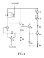
- FIG. 4 is a circuit diagram of the TIA according to the embodiment of the present invention.
- the TIA 110 inputs an AGC signal which has been outputted from AGC 130 via transistors Q1 and Q2. Both ends of each of transistors Q1 and Q2 are connected to resistors Rc and Rf, respectively.
- the bandwidth and trans-impedance gain of the TIA are determined by the resistors Rc and Rf, as explained further with reference to FIG. 6.
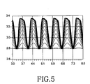
- FIG. 5 shows a wave of the output characteristic of an input current in TIA when AGC is not operating.
- AGC 130 when the AGC 130 does not operate, a considerable output signal distortion occurs if the level of an input current is beyond the range of -31dBm to - 16dBm. As such, the AGC 130 must operate in order to prevent the signal distortion. Note that the AGC 130 must have a waveform which is not distorted regardless of the current input.
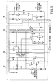
- FIG. 6 is a circuit diagram of the automatic gain controller according to the embodiment of the present invention.
- the AGC 130 detects the level of an output signal and generates an AGC signal, thereby changing the amounts of Rf and Rc according to the amount of an input current.
- the generated AGC signal is applied to the transistors Q1 and Q2 of the TIA 110.
- I-V DC characteristic curve of MOS is utilized.
- Rf and Rc values vary depending on the amount of Vgs (gate-source voltage) applied to the gates of the transistors Q1 and Q2, the bandwidth and gain at a desired input current can be determined selectively.
- the following formulae 1, 2, and 3 are used to obtain an Rf value.
- Vt refers to a threshold voltage
- ⁇ and n refer to electron mobility
- Ci refers to a capacitance per unit area
- W refers to a channel width
- L refers to a channel length.
- Rf and Rc values vary depending on the amount of Vgs applied to the gate.
- the AGC 130 generates an AGC signal when the transistors Q1 and Q2 are turned off by the bottom signal level output from the TIA. Note that a signal begins to be distorted at its bottom signal level during the amplification by the TIA 110. In the embodiment, the AGC 130 begins to operate when an output signal from the TIA 110 begins to be distorted, then the AGC 130 compensates the gain characteristic according to the level of an input signal. As shown in FIG. 6, the AGC 130 comprises a bottom signal level determining section 134, an AGC signal generating section 136, and an output stabilizing buffer 138.
- the bottom signal level determining section 134 consists of a resistor R3 and transistors Q3, Q4, and Q5 and serves to analyzes the bottom level of a signal inputted to the base of the transistor Q1 and determines whether a signal is present. If it is determined that a signal is present, the bottom level determining section 134 will output a "high" signal. If it is determined that no signal is present, the bottom level determining section 134 will generate a reset signal for initialization at intervals between packets.
- the output of the bottom level determining section 134 is connected to the gate of a transistor Q6 of the AGC signal generating section 136.
- the transistor Q6 turns on when its gate voltage is maintained to be high.
- a capacitor C1 connected to the drain of the transistor Q6 is charged to have a voltage of 3 times greater than the diode turn-on voltage.
- the drain voltage of a transistor Q7 becomes "low" to show the presence of a signal.
- the bottom level determining section 134 determines that no signal is present, it will turn the gate voltage of the transistor Q6 of the AGC signal generating section 136 to be "low.”
- the gate voltage is low, the transistor Q6 turns off and begins to be discharged at a voltage of 3 times greater than the diode turn-on voltage.
- the transistor Q6 is kept turned off until the discharge time set by an internal time constant circuit, which is formed by the capacitor C1 and the resistor R4, lapses. Then, the drain voltage of the transistor Q7 becomes "high" to show that no signal is present, which indicates the end of a packet.
- This indication causes a transistor Q8 to be discharged and an AGC signal to be reset so that the AGC voltage level can be reset at the beginning of the next packet. Accordingly, it is possible to prevent problems, such as excessive reduction of the TIA's output when the AGC operation standard level is excessively lowered or operation of the AGC after distortion of an output signal when the standard level is excessively raised.
- FIGs. 7a and 7b show the output voltage characteristic according to the amount of an input current in the TIA when the automatic gain controller generates an automatic gain control signal to adjust the signal distortion.
- FIG. 7a shows the output voltage characteristic when applying 3.0V to the gate of the transistor Q1 and 2.2V to the gate of the transistor Q2 when the level of an input current is -31dBm to -11dBm
- FIG. 7b shows the output voltage characteristic when applying 4.3V to the gate of the transistor Q1 and 3.5V to the gate of the transistor Q2 when the level of an input current is -31dBm to 0dBm.
- the TIA 110 generates an output voltage that is not distorted according to the AGC signal.
- FIG. 8 shows the gain and bandwidth characteristics of the TIA when an AGC signal is generated.
- Curve “A” in FIG. 8 shows the gain and bandwidth characteristics of the TIA when an AGC signal is not generated.
- Curves “B” and “C” show the gain and bandwidth characteristics of the TIA in the cases shown in FIGs. 7a and 7b, respectively.
- the AGC 130 operates when an output signal begins to be distorted during the amplification by the TIA 110. Accordingly, it is possible to prevent problems, such as excessive reduction of the TIA's output when the AGC operation standard level is excessively lowered, or operation of the AGC after the distortion of the output signal when the standard level is excessively raised.
- FIGs. 9a and 9b show that an AGC signal is not generated at a low-level input current, and that an AGC signal is generated when the input current is raised to a sufficient level.
- FIG. 9a shows a case when an input current is 10 ⁇ A
- FIG. 9b shows the generation of an AGC signal when an input current is 100 ⁇ A.
- the automatic gain controller can rapidly respond between packets in a burst-mode operation and correctly determine the presence of a signal.
- the automatic gain controller can greatly reduce the AGC loop time (to tens of nsec at the longest).
Landscapes
- Physics & Mathematics (AREA)
- Electromagnetism (AREA)
- Engineering & Computer Science (AREA)
- Computer Networks & Wireless Communication (AREA)
- Signal Processing (AREA)
- Control Of Amplification And Gain Control (AREA)
- Optical Communication System (AREA)
- Amplifiers (AREA)
Abstract
Description
As shown in FIG. 6, the
Claims (9)
- An automatic gain control device used in an optical receiver, comprising:wherein a drain voltage of said second transistor becomes low when said capacitor is charged but becomes high when said capacitor is discharged.a pre-amplifier for converting an input current signal to a corresponding voltage signal;a bottom signal level detector for generating a signal indicative of the presence of a signal output from the preamplifier and a reset signal for initialization of intervals between packets; andan automatic gain controller for providing an automatic gain control signal in response to an output signal from the bottom signal level detector, said automatic gain controller including a first transistor which turns on according to the output signal from said bottom signal level detector and a second transistor coupled to a capacitor for charging or discharging a voltage applied by said first transistor,
- The automatic gain control device according to claim 1, wherein said automatic gain controller begins to operate when an output signal begins to be distorted during an amplification process by said pre-amplifier.
- The automatic gain control device according to claim 1 or 2, further comprising a third transistor coupled to said second transistor of said automatic gain controller for discharging when the drain voltage is high in order to reset the automatic gain control signal.
- The automatic gain control device according to one of claims 1 to 3, further comprising an optical detector coupled to an input of the preamplifier for detecting an optical signal.
- The automatic gain control device according to one of claims 1 to 4, wherein said preamplifier is a trans-impedance amplifier.
- The automatic gain control device according to one of claims 1 to 5, wherein said first transistor and said second transistor are coupled to a first resistor and a second resistor, respectively, wherein gain and bandwidth of the preamplifier is in dependence of said first and second resistors.
- A burst-mode optical receiver comprising an automatic gain control device according to one of claims 1 to 6.
- An automatic gain control method for operating an optical receiver, the method comprising:wherein said automatic gain controller includes a first transistor to be turned on according to the output signal from said bottom signal level detector and a second transistor coupled to a capacitor for charging or discharging a voltage applied by said first transistor,converting an input current signal to a corresponding voltage signal by a pre-amplifier;generating a signal by a bottom signal level detector, wherein said signal is indicative of the presence of a signal output from the pre-amplifier;generating a reset signal by the bottom signal level detector for initializing intervals between packets; andproviding an automatic gain control signal by an automatic gain controller in response to an output signal from the bottom signal level detector,
wherein a drain voltage of said second transistor becomes low when said capacitor is charged but becomes high when said capacitor is discharged. - The method of claim 8 adapted to operate the device according to one of claims 1 to 6.
Applications Claiming Priority (2)
| Application Number | Priority Date | Filing Date | Title |
|---|---|---|---|
| KR2002023065 | 2002-04-26 | ||
| KR1020020023065A KR100630083B1 (en) | 2002-04-26 | 2002-04-26 | Automatic Gain Control Device for Burst Mode Optical Receiver |
Publications (3)
| Publication Number | Publication Date |
|---|---|
| EP1357665A2 true EP1357665A2 (en) | 2003-10-29 |
| EP1357665A3 EP1357665A3 (en) | 2004-03-17 |
| EP1357665B1 EP1357665B1 (en) | 2005-09-28 |
Family
ID=28786980
Family Applications (1)
| Application Number | Title | Priority Date | Filing Date |
|---|---|---|---|
| EP03009431A Expired - Lifetime EP1357665B1 (en) | 2002-04-26 | 2003-04-25 | Automatic gain control device for a burst-mode optical receiver |
Country Status (5)
| Country | Link |
|---|---|
| US (1) | US6911644B2 (en) |
| EP (1) | EP1357665B1 (en) |
| JP (1) | JP2003332866A (en) |
| KR (1) | KR100630083B1 (en) |
| DE (1) | DE60301685T2 (en) |
Cited By (2)
| Publication number | Priority date | Publication date | Assignee | Title |
|---|---|---|---|---|
| EP2391003A1 (en) | 2010-05-24 | 2011-11-30 | University College Cork | Linear burst mode receiver |
| WO2012160230A1 (en) * | 2011-05-26 | 2012-11-29 | Consejo Superior De Investigaciones Científicas (Csic) | Low-mismatch and low-consumption transimpedance gain circuit for temporally differentiating photo-sensing systems in dynamic vision sensors |
Families Citing this family (23)
| Publication number | Priority date | Publication date | Assignee | Title |
|---|---|---|---|---|
| KR100554163B1 (en) * | 2003-03-29 | 2006-02-22 | 한국전자통신연구원 | Burst Mode Optical Receiver Considering Extinction Ratio Characteristics of Received Optical Signals |
| KR100537902B1 (en) * | 2003-03-29 | 2005-12-20 | 한국전자통신연구원 | Bust mode optical signal receiving apparatus |
| KR100547840B1 (en) * | 2003-06-04 | 2006-01-31 | 삼성전자주식회사 | Automatic Gain Control with Fast Settling Time |
| CN1820413B (en) * | 2003-07-30 | 2012-10-31 | 三菱电机株式会社 | Gain Switching Circuit of Preamplifier |
| JP2006080988A (en) * | 2004-09-10 | 2006-03-23 | Sumitomo Electric Ind Ltd | Preamplifier |
| WO2006013893A1 (en) * | 2004-08-03 | 2006-02-09 | Nippon Telegraph And Telephone Corporation | Transimpedance amplifier |
| US7505739B2 (en) * | 2004-11-12 | 2009-03-17 | Atheros Technology Ltd. | Automatic mode setting and power ramp compensator for system power on conditions |
| KR100703389B1 (en) * | 2004-12-03 | 2007-04-03 | 삼성전자주식회사 | Burst mode optical receiver and method |
| JP4546348B2 (en) * | 2005-07-22 | 2010-09-15 | 日本電信電話株式会社 | Transimpedance amplifier |
| US7702044B2 (en) * | 2005-12-05 | 2010-04-20 | Marvell World Trade, Ltd. | Radar detection and dynamic frequency selection |
| KR100826882B1 (en) * | 2005-12-05 | 2008-05-06 | 한국전자통신연구원 | Digital automatic gain controller method and apparatus in bust mode optical receiver |
| US7889815B2 (en) * | 2007-02-13 | 2011-02-15 | Optical Communication Products, Inc. | Burst mode receiver for passive optical network |
| KR100972033B1 (en) * | 2008-08-13 | 2010-07-23 | 한국전자통신연구원 | Burst Mode Receiver for Gigabit Passive Optical Networks with Single and Preamplifier Integrated |
| US20100150561A1 (en) * | 2008-12-12 | 2010-06-17 | Seung-Hyun Cho | Optical receiver, optical line terminal and method of recovering received signals |
| CN101588204A (en) * | 2009-06-23 | 2009-11-25 | 上海华魏光纤传感技术有限公司 | Wideband high-sensitivity optical receiver |
| US9325426B2 (en) | 2013-07-11 | 2016-04-26 | Avago Technologies General Ip (Singapore) Pte. Ltd. | Burst-mode receiver having a wide dynamic range and low pulse-width distortion and a method |
| CN105432030B (en) * | 2013-08-07 | 2017-12-29 | 三菱电机株式会社 | Current-voltage conversion circuit, optical receiver and optical terminal device |
| CN104956654B (en) * | 2013-11-12 | 2018-09-18 | 康斯乔最高科学研究公司 | Method and apparatus for detecting the light intensity time-varying in photosensor matrix |
| JP6096650B2 (en) * | 2013-12-16 | 2017-03-15 | 日本電信電話株式会社 | Transimpedance amplifier, core circuit, and gain control circuit |
| CN103929139B (en) * | 2014-04-22 | 2016-10-12 | 西安电子科技大学 | The transimpedance preamplifier of the photoreceiver of High Precision Automatic gain control |
| US20160077134A1 (en) * | 2014-09-12 | 2016-03-17 | Qualcomm Incorporated | Enhanced radar detection for communication networks |
| US10079584B1 (en) | 2017-03-14 | 2018-09-18 | Futurewei Technologies, Inc. | Closed-loop automatic gain control in linear burst-mode transimpedance amplifier |
| US12552105B2 (en) | 2021-06-29 | 2026-02-17 | General Electric Company | Alignment of energy beams in additive manufacturing systems and machines |
Family Cites Families (12)
| Publication number | Priority date | Publication date | Assignee | Title |
|---|---|---|---|---|
| CA2106439A1 (en) * | 1992-11-13 | 1994-05-14 | Yusuke Ota | Burst mode digital data receiver |
| JP2889803B2 (en) * | 1993-11-22 | 1999-05-10 | 三洋電機株式会社 | Level setting circuit |
| JPH10173456A (en) * | 1996-12-11 | 1998-06-26 | Fujitsu Ltd | Signal amplification circuit |
| JP3504176B2 (en) | 1998-12-02 | 2004-03-08 | 富士通株式会社 | Signal amplification circuit |
| JP3329302B2 (en) * | 1999-02-26 | 2002-09-30 | 日本電気株式会社 | Automatic gain switching type burst optical receiver |
| JP3259707B2 (en) * | 1999-02-26 | 2002-02-25 | 日本電気株式会社 | Burst mode optical receiver with AGC |
| WO2001048914A1 (en) * | 1999-12-27 | 2001-07-05 | Fujitsu Limited | Signal amplifying circuit and optical signal receiver using the same |
| CA2297716C (en) * | 2000-01-31 | 2004-10-26 | Leitch Technology Corporation | Automatic gain control circuit and optical receiver |
| JP3947865B2 (en) * | 2000-03-06 | 2007-07-25 | 富士通株式会社 | Preamplifier |
| US6404281B1 (en) * | 2000-11-14 | 2002-06-11 | Sirenza Microdevices, Inc. | Wide dynamic range transimpedance amplifier |
| KR100630089B1 (en) * | 2002-04-15 | 2006-09-27 | 삼성전자주식회사 | Burstmode Optical Receiver with Differential Output Structure |
| KR100640413B1 (en) * | 2002-04-16 | 2006-10-30 | 삼성전자주식회사 | Burstmode Optical Receiver |
-
2002
- 2002-04-26 KR KR1020020023065A patent/KR100630083B1/en not_active Expired - Fee Related
-
2003
- 2003-03-14 US US10/389,058 patent/US6911644B2/en not_active Expired - Fee Related
- 2003-04-25 EP EP03009431A patent/EP1357665B1/en not_active Expired - Lifetime
- 2003-04-25 DE DE60301685T patent/DE60301685T2/en not_active Expired - Lifetime
- 2003-04-28 JP JP2003124434A patent/JP2003332866A/en active Pending
Cited By (5)
| Publication number | Priority date | Publication date | Assignee | Title |
|---|---|---|---|---|
| EP2391003A1 (en) | 2010-05-24 | 2011-11-30 | University College Cork | Linear burst mode receiver |
| WO2011147807A1 (en) | 2010-05-24 | 2011-12-01 | University College Cork - National University Of Ireland, Cork | Linear burst mode receiver |
| US9059807B2 (en) | 2010-05-24 | 2015-06-16 | University College Cork—National University of Ireland | Linear burst mode receiver |
| WO2012160230A1 (en) * | 2011-05-26 | 2012-11-29 | Consejo Superior De Investigaciones Científicas (Csic) | Low-mismatch and low-consumption transimpedance gain circuit for temporally differentiating photo-sensing systems in dynamic vision sensors |
| US9681081B2 (en) | 2011-05-26 | 2017-06-13 | Consejo Superior De Investigaciones Cientificas (Csic) | Transimpedance gain circuit for temporally differentiating photo-sensing systems in dynamic vision sensors |
Also Published As
| Publication number | Publication date |
|---|---|
| US6911644B2 (en) | 2005-06-28 |
| DE60301685D1 (en) | 2006-02-09 |
| JP2003332866A (en) | 2003-11-21 |
| KR20030084382A (en) | 2003-11-01 |
| EP1357665B1 (en) | 2005-09-28 |
| DE60301685T2 (en) | 2006-03-16 |
| EP1357665A3 (en) | 2004-03-17 |
| US20030201382A1 (en) | 2003-10-30 |
| KR100630083B1 (en) | 2006-09-27 |
Similar Documents
| Publication | Publication Date | Title |
|---|---|---|
| EP1357665B1 (en) | Automatic gain control device for a burst-mode optical receiver | |
| US6909082B2 (en) | Automatic threshold control device for burst mode optical receiver | |
| US7218865B2 (en) | Burst-mode optical receiver of differential output structure | |
| US8248165B2 (en) | Amplifier and optical module performing gain control | |
| JP3749718B2 (en) | Burst mode optical receiver | |
| US7330670B2 (en) | Bottom level detection device for burst mode optical receiver | |
| US8948610B2 (en) | Data signal threshold detection and/or recovery in optical and/or optoelectric receivers and/or transceivers | |
| JP2010166216A (en) | Preamplifier | |
| US7583904B2 (en) | Transimpedance (TIA) circuit usable for burst mode communications | |
| US7206521B2 (en) | Signal level detecting device for a burst-mode optical receiver | |
| KR20040084623A (en) | Bust mode optical signal receiving apparatus | |
| KR100547840B1 (en) | Automatic Gain Control with Fast Settling Time | |
| US7323938B2 (en) | Amplifier circuit and light receiving apparatus | |
| JP2007336223A (en) | Signal level detecting device, optical receiving device, and signal level detecting method |
Legal Events
| Date | Code | Title | Description |
|---|---|---|---|
| PUAI | Public reference made under article 153(3) epc to a published international application that has entered the european phase |
Free format text: ORIGINAL CODE: 0009012 |
|
| 17P | Request for examination filed |
Effective date: 20030425 |
|
| AK | Designated contracting states |
Kind code of ref document: A2 Designated state(s): AT BE BG CH CY CZ DE DK EE ES FI FR GB GR HU IE IT LI LU MC NL PT RO SE SI SK TR |
|
| AX | Request for extension of the european patent |
Extension state: AL LT LV MK |
|
| PUAL | Search report despatched |
Free format text: ORIGINAL CODE: 0009013 |
|
| AK | Designated contracting states |
Kind code of ref document: A3 Designated state(s): AT BE BG CH CY CZ DE DK EE ES FI FR GB GR HU IE IT LI LU MC NL PT RO SE SI SK TR |
|
| AX | Request for extension of the european patent |
Extension state: AL LT LV MK |
|
| RIC1 | Information provided on ipc code assigned before grant |
Ipc: 7H 03G 3/30 A Ipc: 7H 03F 3/08 B |
|
| AKX | Designation fees paid |
Designated state(s): DE FR GB |
|
| GRAP | Despatch of communication of intention to grant a patent |
Free format text: ORIGINAL CODE: EPIDOSNIGR1 |
|
| 17Q | First examination report despatched |
Effective date: 20040901 |
|
| GRAS | Grant fee paid |
Free format text: ORIGINAL CODE: EPIDOSNIGR3 |
|
| GRAA | (expected) grant |
Free format text: ORIGINAL CODE: 0009210 |
|
| AK | Designated contracting states |
Kind code of ref document: B1 Designated state(s): DE FR GB |
|
| REG | Reference to a national code |
Ref country code: GB Ref legal event code: FG4D |
|
| REF | Corresponds to: |
Ref document number: 60301685 Country of ref document: DE Date of ref document: 20060209 Kind code of ref document: P |
|
| ET | Fr: translation filed | ||
| PLBE | No opposition filed within time limit |
Free format text: ORIGINAL CODE: 0009261 |
|
| STAA | Information on the status of an ep patent application or granted ep patent |
Free format text: STATUS: NO OPPOSITION FILED WITHIN TIME LIMIT |
|
| 26N | No opposition filed |
Effective date: 20060629 |
|
| REG | Reference to a national code |
Ref country code: FR Ref legal event code: PLFP Year of fee payment: 14 |
|
| PGFP | Annual fee paid to national office [announced via postgrant information from national office to epo] |
Ref country code: GB Payment date: 20160311 Year of fee payment: 14 |
|
| PGFP | Annual fee paid to national office [announced via postgrant information from national office to epo] |
Ref country code: DE Payment date: 20160421 Year of fee payment: 14 |
|
| PGFP | Annual fee paid to national office [announced via postgrant information from national office to epo] |
Ref country code: FR Payment date: 20160415 Year of fee payment: 14 |
|
| REG | Reference to a national code |
Ref country code: DE Ref legal event code: R119 Ref document number: 60301685 Country of ref document: DE |
|
| GBPC | Gb: european patent ceased through non-payment of renewal fee |
Effective date: 20170425 |
|
| REG | Reference to a national code |
Ref country code: FR Ref legal event code: ST Effective date: 20171229 |
|
| PG25 | Lapsed in a contracting state [announced via postgrant information from national office to epo] |
Ref country code: DE Free format text: LAPSE BECAUSE OF NON-PAYMENT OF DUE FEES Effective date: 20171103 Ref country code: FR Free format text: LAPSE BECAUSE OF NON-PAYMENT OF DUE FEES Effective date: 20170502 |
|
| PG25 | Lapsed in a contracting state [announced via postgrant information from national office to epo] |
Ref country code: GB Free format text: LAPSE BECAUSE OF NON-PAYMENT OF DUE FEES Effective date: 20170425 |