EP1357637A2 - Spiral wound, series fed, array antenna - Google Patents
Spiral wound, series fed, array antenna Download PDFInfo
- Publication number
- EP1357637A2 EP1357637A2 EP03007821A EP03007821A EP1357637A2 EP 1357637 A2 EP1357637 A2 EP 1357637A2 EP 03007821 A EP03007821 A EP 03007821A EP 03007821 A EP03007821 A EP 03007821A EP 1357637 A2 EP1357637 A2 EP 1357637A2
- Authority
- EP
- European Patent Office
- Prior art keywords
- antenna
- spiral
- phased array
- circuit board
- arms
- Prior art date
- Legal status (The legal status is an assumption and is not a legal conclusion. Google has not performed a legal analysis and makes no representation as to the accuracy of the status listed.)
- Withdrawn
Links
- 230000009977 dual effect Effects 0.000 claims description 8
- 238000000034 method Methods 0.000 claims description 5
- 238000003491 array Methods 0.000 description 11
- 230000008901 benefit Effects 0.000 description 4
- 238000004806 packaging method and process Methods 0.000 description 3
- 238000010276 construction Methods 0.000 description 2
- 230000000694 effects Effects 0.000 description 2
- 238000012986 modification Methods 0.000 description 2
- 230000004048 modification Effects 0.000 description 2
- 230000000737 periodic effect Effects 0.000 description 2
- 230000010363 phase shift Effects 0.000 description 2
- 230000003321 amplification Effects 0.000 description 1
- 238000001816 cooling Methods 0.000 description 1
- 230000008878 coupling Effects 0.000 description 1
- 238000010168 coupling process Methods 0.000 description 1
- 238000005859 coupling reaction Methods 0.000 description 1
- 238000001914 filtration Methods 0.000 description 1
- 238000004519 manufacturing process Methods 0.000 description 1
- 238000003199 nucleic acid amplification method Methods 0.000 description 1
- 230000010287 polarization Effects 0.000 description 1
- 230000000135 prohibitive effect Effects 0.000 description 1
Images


Classifications
-
- H—ELECTRICITY
- H01—ELECTRIC ELEMENTS
- H01Q—ANTENNAS, i.e. RADIO AERIALS
- H01Q21/00—Antenna arrays or systems
- H01Q21/0087—Apparatus or processes specially adapted for manufacturing antenna arrays
-
- H—ELECTRICITY
- H01—ELECTRIC ELEMENTS
- H01Q—ANTENNAS, i.e. RADIO AERIALS
- H01Q21/00—Antenna arrays or systems
- H01Q21/0006—Particular feeding systems
-
- H—ELECTRICITY
- H01—ELECTRIC ELEMENTS
- H01Q—ANTENNAS, i.e. RADIO AERIALS
- H01Q21/00—Antenna arrays or systems
- H01Q21/0006—Particular feeding systems
- H01Q21/0037—Particular feeding systems linear waveguide fed arrays
- H01Q21/0043—Slotted waveguides
- H01Q21/005—Slotted waveguides arrays
- H01Q21/0056—Conically or cylindrically arrayed
-
- H—ELECTRICITY
- H01—ELECTRIC ELEMENTS
- H01Q—ANTENNAS, i.e. RADIO AERIALS
- H01Q9/00—Electrically-short antennas having dimensions not more than twice the operating wavelength and consisting of conductive active radiating elements
- H01Q9/04—Resonant antennas
- H01Q9/16—Resonant antennas with feed intermediate between the extremities of the antenna, e.g. centre-fed dipole
- H01Q9/26—Resonant antennas with feed intermediate between the extremities of the antenna, e.g. centre-fed dipole with folded element or elements, the folded parts being spaced apart a small fraction of operating wavelength
- H01Q9/27—Spiral antennas
Definitions
- the present invention relates to phased array antennae, and more particularly, this invention relates to series fed phased array antennae.
- phased array antennae are required on naval ships, land based radar stations and similar areas. Some traditional phased array antennae use periodic or spiral lattices and transmit/receive modules that are prohibitive in cost. When an antenna is designed for use with short wavelengths in advanced radar designs, a low side lobe architecture is required.
- phased array antenna architecture uses a Dual Application Program (DUAP) array structure based on a typical dual beam and corporate radio frequency and digital feed network. It typically includes a multilayer circuit board having various layers for different circuit components, including low noise amplifiers, phase shifters and other assorted feed lines, signal traces and component devices.
- DUAP Dual Application Program
- this type of antenna structure requires a complicated printed wiring board having multiple interconnects. For example, some printed wiring boards include over two thousand (2,000) vias in an 18-inch square printed circuit card, 64 elements, and two antenna beams. Not only is the layout of this array difficult to achieve, it can surpass some existing radio frequency layout tool capacities.
- This type of antenna architecture also requires a complicated feed network and multilayer circuit board with complicated circuit components that should not cross-over, thus, increasing design and construction difficulty.
- phased array antennae use corporate feed networks with complicated interconnect systems because a corporate fed antenna allows a wide bandwidth. Also, in a planar array having a corporate feed network, the periodic spacing and phase settings between the antenna elements require only a simple sine calculation.
- the corporate feed network can typically provide an advantageous impedance match. Unfortunately, a corporate feed network is usually complicated and is often designed into an antenna structure from habit and not from advantage.
- linear, series fed array will not have the complicated design drawbacks associated with a corporate feed network.
- Some linear, series fed arrays have been built as early as the 1940's. For example, the United States Navy built a phased array series of fed WG slot arrays used to scan the beam. These type of linear, series fed arrays, however, were limited in their use because of frequency scan effects and the grating lobes.
- a phased array antenna that includes a circuit board and a balanced, series fed antenna array formed from a plurality of antenna elements positioned in at least two spiral antenna arms on the circuit board. At least one signal feed point is positioned at a center portion of the spiral antenna arms for series feeding the antenna array, such that the antenna aids in breaking up frequency scan and grating lobes.
- electronic circuitry can be supported by the circuit board and operatively connected to the antenna elements for amplifying, phase shifting and beam forming any transmitted or received signals.
- the antenna array is formed as two balanced series fed antenna arrays, each formed as spiral antenna arms and having dual feed points.
- the circuit board could be formed as a multilayer circuit board having a microstrip layer operative with the antenna elements for series driving the antenna array.
- the number of antenna elements within each spiral antenna arm are substantially the same and can be formed as either surface mounted antenna elements or printed antenna elements.
- the plurality of antenna elements are arranged on the circuit board in four spiral antenna arms as balanced, series fed antenna arrays having signal feed points at a center portion of the spiral arm.
- the antenna elements can be formed as respective 0, 90, 180 and 270 degree spiral arms for phased operation.
- the phased array antenna can comprise a balanced, series fed antenna array formed from a plurality of antenna elements positioned in at least two spiral antenna arms on the circuit board and having at least one signal feed point at a center portion of the spiral antenna arms for series feeding the antenna array.
- the spiral arms can be formed from a waveguide having slots defining the antenna elements. If a waveguide is not used, then the antenna elements can be positioned on a planar circuit board as described before.
- FIG. 1 is a fragmentary view of a linear, series fed array antenna showing individual antenna elements that can be controlled by appropriate phase shift devices.
- FIGS. 2-5 are fragmentary, plan views of the respective spiral arms shown as a single spiral arm in FIGS. 2 and 4 and dual spiral arms in FIGS. 4 and 5.
- FIG. 6 is a fragmentary plan view of two balanced, series fed arrays such as shown in FIGS. 3 and 5 that are wrapped in a spiral configuration with 0, 90, 180, and 270 degree spiral arms.
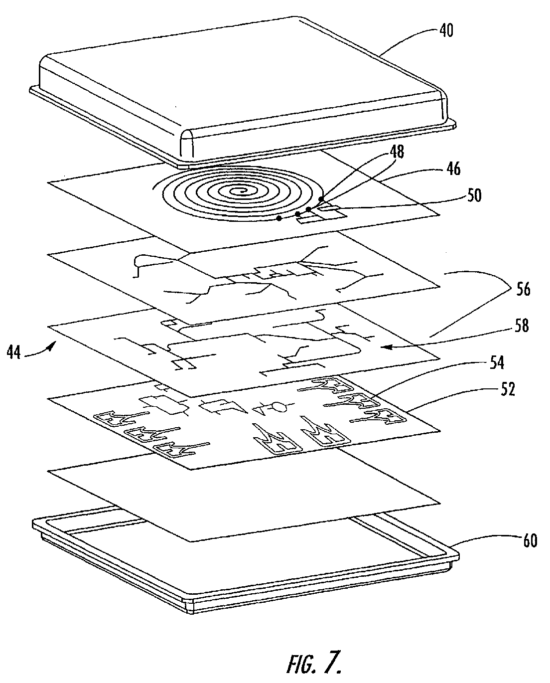
- FIG. 7 is an exploded, isometric view of the series fed phased array antenna of the present invention as formed from a single, multilayer printed circuit board and showing different layers for supporting various amplifier elements, beam forming network, phase shifters and packaging components.
- FIG. 8 illustrates a waveguide that could be configured in a spiral configuration in accordance with the present invention.
- the present invention advantageously provides a phased array antenna that includes a balanced, series fed, phased array antenna formed from a plurality of antenna elements positioned in at least two spiral antenna arms on a circuit board. At least one signal feed point is provided at a center portion of the spiral antenna arms for series feeding the antenna array and conducting any transmitted or received signals to aid in breaking up frequency scan and grating lobes.
- This new class of series fed antenna array is advantageous over prior art linear, series fed antenna arrays that do not break up the frequency scan and grating lobes as in the present invention.
- the present invention also simplifies the physical construction of an array antenna built on printed circuit boards and cuts non-reoccurring engineering (NRE) costs while allowing a simple layout for antenna elements, signal feed circuits, and associated components.
- NRE non-reoccurring engineering
- the spiral configuration of the present invention can be applied to numerous multiple beam lengths, including TCDL, CDL-N, and DD XX structures.
- the design of the present invention can cut costs and non-reoccurring engineering aspects on all arrays with estimated cuts of 50% and schedule cuts of six months. Production cuts can be lowered from about 10% to about 50%.
- FIG. 1 illustrates at 10 a prior art linear, series fed array antenna having numerous interconnected antenna elements 12 using phase shift components 14 (shown by the arrow) and other driving elements and signal circuits as known to those skilled in the art.
- This type of linear, series fed array could be formed on a multilayer circuit board by techniques as known to those skilled in the art.
- a feed point 16 is positioned at the center of the linear array 10 and includes two signal feed line terminals 18,20 in which a signal voltage is placed across the terminals as known to those skilled in the art.
- the array is terminated at either end by appropriate terminations 22 to ground.
- a phased array antenna is formed as series fed antenna array 30 (FIG. 6) that is wound in a spiral as shown in the various spiral arms of FIGS. 2-5.
- One spiral arm is shown in FIG. 2 and depicts a closely spaced single spiral arm, with FIG. 3 illustrating the two spiral arms formed when the linear array as in FIG. 1 is wrapped about itself in a spiral with feed points positioned in the center portion and forming a balanced, series fed array.
- FIG. 4 shows a loosely formed single spiral arm for the spiral arms shown in FIG. 5 and forming a second, balanced, series fed array. The spiral arms combine together to form a spiral series fed array 30 as shown in FIG.
- FIG. 6 shows two balanced, series fed arrays wrapped in the spiral configuration that breaks up frequency scan and grating lobes.
- a pair of dual feed points or four signal feed "starts" 32a, 32b, 34a, 34b are shown for each dual spiral that could be formed from two linear, series fed antennae wound in a spiral.
- the illustrated spiral wound series fed antenna shown in FIG. 6 has the four signal feed points or starts 32a, 32b, 34a, 34b and four spiral arms 36a, 36b, 38a, 38b with over one thousand (1,000) antenna elements.
- This structure forms a quad drive having dual feed points for the four starts as illustrated.
- the illustrated four spiral arms 36a, 36b, 38a, 38b having the four spiral signal feed starts 32a, 32b, 34a, 34b have antenna elements that are positioned on the circuit board and spiral wound to form a respective 0 degree spiral arms as 36b ; a 90 degree spiral arm as 36a ; a 180 degree spiral arm as 38a ; and a 270 degree spiral arm as 38b .
- the illustrated antenna structure has a high aperture efficiency using 0.63662 wavelength spacing with 7.7815 dBi antenna elements in one non-limiting example. Numerical wavelength lamda values are shown on the respective x,y axis with respect to the positioning of the various antenna elements.
- a non-limiting example of a lattice support structure for the antenna of the present invention is shown in FIG. 7, and could include a radome 40 and radiating antenna elements formed in the spiral configuration as a series fed array and positioned on one multilayer circuit board 44 .
- a top layer 46 of the board includes the antenna elements 48 , and in some designs, even amplifier elements 50 , including low noise amplifiers (LNA) or other components.
- the antenna elements 48 can be surface mounted or printed by techniques known to those skilled in the art.
- a bottom layer portion 52 of the board can include, for instance, phase shifters, post amplification circuit elements with combiners and beam steering elements and other components 54 .
- a middle layer portion 56 (such as two layers) can include a beam former network with power combining and signal distribution 58 .
- Other layers can include beam control components, filtering or other components, which can exist combined on some layers or on separate layers.
- One or more microstrip layers are operative for conducting signals and driving the array.
- the layers can be formed by techniques known to those skilled in the art, including green tape layers.
- Mechanical packaging components 60 can include basic power supplies, cooling circuits and packaging. Such a structure can then be placed in another support structure and form part of a lattice as an integral element.
- FIG. 8 illustrates a waveguide 70 such as known to those skilled in the art that can be wound in a spiral to form a spiral wound, series fed array.
- the waveguide 70 includes a feed 72 and a plurality of slots 74 as known to those skilled in the art.
- the slots 74 could be less vertical as they extend from the center portion of the waveguide. Coupling could be a function of the angle of the slot.
- the present invention now provides a series fed array antenna wrapped in a spiral configuration that is advantageous over prior art linear, series fed arrays to break up frequency scan and grating lobes.
Landscapes
- Engineering & Computer Science (AREA)
- Manufacturing & Machinery (AREA)
- Variable-Direction Aerials And Aerial Arrays (AREA)
- Waveguide Aerials (AREA)
- Radar Systems Or Details Thereof (AREA)
Abstract
Description
- The present invention relates to phased array antennae, and more particularly, this invention relates to series fed phased array antennae.
- Low cost phased array antennae are required on naval ships, land based radar stations and similar areas. Some traditional phased array antennae use periodic or spiral lattices and transmit/receive modules that are prohibitive in cost. When an antenna is designed for use with short wavelengths in advanced radar designs, a low side lobe architecture is required.
- One type of phased array antenna architecture uses a Dual Application Program (DUAP) array structure based on a typical dual beam and corporate radio frequency and digital feed network. It typically includes a multilayer circuit board having various layers for different circuit components, including low noise amplifiers, phase shifters and other assorted feed lines, signal traces and component devices. For multiple beam and multiple polarization arrays, however, this type of antenna structure requires a complicated printed wiring board having multiple interconnects. For example, some printed wiring boards include over two thousand (2,000) vias in an 18-inch square printed circuit card, 64 elements, and two antenna beams. Not only is the layout of this array difficult to achieve, it can surpass some existing radio frequency layout tool capacities. This type of antenna architecture also requires a complicated feed network and multilayer circuit board with complicated circuit components that should not cross-over, thus, increasing design and construction difficulty.
- Many phased array antennae use corporate feed networks with complicated interconnect systems because a corporate fed antenna allows a wide bandwidth. Also, in a planar array having a corporate feed network, the periodic spacing and phase settings between the antenna elements require only a simple sine calculation. The corporate feed network can typically provide an advantageous impedance match. Unfortunately, a corporate feed network is usually complicated and is often designed into an antenna structure from habit and not from advantage.
- A linear, series fed array, however, will not have the complicated design drawbacks associated with a corporate feed network. Some linear, series fed arrays have been built as early as the 1940's. For example, the United States Navy built a phased array series of fed WG slot arrays used to scan the beam. These type of linear, series fed arrays, however, were limited in their use because of frequency scan effects and the grating lobes.
- In view of the foregoing background, it is therefore an object of the present invention to provide a series fed array antenna that overcomes the drawbacks associated with prior art linear series fed array antennae.
- It is also an object of the present invention to provide a series fed antenna array that breaks up frequency scan effects and grating lobes.
- It is yet another object of the present invention to provide a low cost antenna array that simplifies layout and eliminates crossover drawbacks associated complicated corporate feed networks.
- These and other objects, features and advantages in accordance with the present invention are provided by a phased array antenna that includes a circuit board and a balanced, series fed antenna array formed from a plurality of antenna elements positioned in at least two spiral antenna arms on the circuit board. At least one signal feed point is positioned at a center portion of the spiral antenna arms for series feeding the antenna array, such that the antenna aids in breaking up frequency scan and grating lobes. In one aspect of the present invention, electronic circuitry can be supported by the circuit board and operatively connected to the antenna elements for amplifying, phase shifting and beam forming any transmitted or received signals.
- In another aspect of the present invention, the antenna array is formed as two balanced series fed antenna arrays, each formed as spiral antenna arms and having dual feed points. The circuit board could be formed as a multilayer circuit board having a microstrip layer operative with the antenna elements for series driving the antenna array. The number of antenna elements within each spiral antenna arm are substantially the same and can be formed as either surface mounted antenna elements or printed antenna elements.
- In yet another aspect of the present invention, the plurality of antenna elements are arranged on the circuit board in four spiral antenna arms as balanced, series fed antenna arrays having signal feed points at a center portion of the spiral arm. The antenna elements can be formed as respective 0, 90, 180 and 270 degree spiral arms for phased operation.
- In yet another aspect of the present invention, the phased array antenna can comprise a balanced, series fed antenna array formed from a plurality of antenna elements positioned in at least two spiral antenna arms on the circuit board and having at least one signal feed point at a center portion of the spiral antenna arms for series feeding the antenna array. The spiral arms can be formed from a waveguide having slots defining the antenna elements. If a waveguide is not used, then the antenna elements can be positioned on a planar circuit board as described before.
- Other objects, features and advantages of the present invention will become apparent from the detailed description of the invention which follows, when considered in light of the accompanying drawings in which:
- FIG. 1 is a fragmentary view of a linear, series fed array antenna showing individual antenna elements that can be controlled by appropriate phase shift devices.
- FIGS. 2-5 are fragmentary, plan views of the respective spiral arms shown as a single spiral arm in FIGS. 2 and 4 and dual spiral arms in FIGS. 4 and 5.
- FIG. 6 is a fragmentary plan view of two balanced, series fed arrays such as shown in FIGS. 3 and 5 that are wrapped in a spiral configuration with 0, 90, 180, and 270 degree spiral arms.
- FIG. 7 is an exploded, isometric view of the series fed phased array antenna of the present invention as formed from a single, multilayer printed circuit board and showing different layers for supporting various amplifier elements, beam forming network, phase shifters and packaging components.
- FIG. 8 illustrates a waveguide that could be configured in a spiral configuration in accordance with the present invention.
- The present invention will now be described more fully hereinafter with reference to the accompanying drawings, in which preferred embodiments of the invention are shown. This invention may, however, be embodied in many different forms and should not be construed as limited to the embodiments set forth herein. Rather, these embodiments are provided so that this disclosure will be thorough and complete, and will fully convey the scope of the invention to those skilled in the art. Like numbers refer to like elements throughout, and prime notation is used to indicate similar elements in alternative embodiments.
- The present invention advantageously provides a phased array antenna that includes a balanced, series fed, phased array antenna formed from a plurality of antenna elements positioned in at least two spiral antenna arms on a circuit board. At least one signal feed point is provided at a center portion of the spiral antenna arms for series feeding the antenna array and conducting any transmitted or received signals to aid in breaking up frequency scan and grating lobes.
- This new class of series fed antenna array is advantageous over prior art linear, series fed antenna arrays that do not break up the frequency scan and grating lobes as in the present invention. The present invention also simplifies the physical construction of an array antenna built on printed circuit boards and cuts non-reoccurring engineering (NRE) costs while allowing a simple layout for antenna elements, signal feed circuits, and associated components. The spiral configuration of the present invention can be applied to numerous multiple beam lengths, including TCDL, CDL-N, and DD XX structures. The design of the present invention can cut costs and non-reoccurring engineering aspects on all arrays with estimated cuts of 50% and schedule cuts of six months. Production cuts can be lowered from about 10% to about 50%.
- FIG. 1 illustrates at 10 a prior art linear, series fed array antenna having numerous interconnected
antenna elements 12 using phase shift components 14 (shown by the arrow) and other driving elements and signal circuits as known to those skilled in the art. This type of linear, series fed array could be formed on a multilayer circuit board by techniques as known to those skilled in the art. Afeed point 16 is positioned at the center of thelinear array 10 and includes two signalfeed line terminals appropriate terminations 22 to ground. - In accordance with the present invention, a phased array antenna is formed as series fed antenna array 30 (FIG. 6) that is wound in a spiral as shown in the various spiral arms of FIGS. 2-5. One spiral arm is shown in FIG. 2 and depicts a closely spaced single spiral arm, with FIG. 3 illustrating the two spiral arms formed when the linear array as in FIG. 1 is wrapped about itself in a spiral with feed points positioned in the center portion and forming a balanced, series fed array. FIG. 4 shows a loosely formed single spiral arm for the spiral arms shown in FIG. 5 and forming a second, balanced, series fed array. The spiral arms combine together to form a spiral series fed
array 30 as shown in FIG. 6, and showing two balanced, series fed arrays wrapped in the spiral configuration that breaks up frequency scan and grating lobes. A pair of dual feed points or four signal feed "starts" 32a, 32b, 34a, 34b are shown for each dual spiral that could be formed from two linear, series fed antennae wound in a spiral. The illustrated spiral wound series fed antenna shown in FIG. 6 has the four signal feed points or starts 32a, 32b, 34a, 34b and fourspiral arms spiral arms - A non-limiting example of a lattice support structure for the antenna of the present invention is shown in FIG. 7, and could include a
radome 40 and radiating antenna elements formed in the spiral configuration as a series fed array and positioned on onemultilayer circuit board 44. Atop layer 46 of the board includes theantenna elements 48, and in some designs, evenamplifier elements 50, including low noise amplifiers (LNA) or other components. Theantenna elements 48 can be surface mounted or printed by techniques known to those skilled in the art. Abottom layer portion 52 of the board can include, for instance, phase shifters, post amplification circuit elements with combiners and beam steering elements andother components 54. A middle layer portion 56 (such as two layers) can include a beam former network with power combining and signaldistribution 58. Other layers can include beam control components, filtering or other components, which can exist combined on some layers or on separate layers. One or more microstrip layers are operative for conducting signals and driving the array. The layers can be formed by techniques known to those skilled in the art, including green tape layers.Mechanical packaging components 60 can include basic power supplies, cooling circuits and packaging. Such a structure can then be placed in another support structure and form part of a lattice as an integral element. - FIG. 8 illustrates a
waveguide 70 such as known to those skilled in the art that can be wound in a spiral to form a spiral wound, series fed array. Thewaveguide 70 includes afeed 72 and a plurality ofslots 74 as known to those skilled in the art. Theslots 74 could be less vertical as they extend from the center portion of the waveguide. Coupling could be a function of the angle of the slot. - It is evident that the present invention now provides a series fed array antenna wrapped in a spiral configuration that is advantageous over prior art linear, series fed arrays to break up frequency scan and grating lobes.
- Many modifications and other embodiments of the invention will come to the mind of one skilled in the art having the benefit of the teachings presented in the foregoing descriptions and the associated drawings. Therefore, it is understood that the invention is not to be limited to the specific embodiments disclosed, and that modifications and embodiments are intended to be included within the scope of the appended claims.
Claims (11)
- A phased array antenna comprising a balanced, series fed antenna array formed from a plurality of antenna elements positioned in at least two spiral antenna arms on the circuit board and having at least one signal feedpoint at a center portion of the spiral antenna arms for series feeding the antenna array.
- A phased array antenna according to Claim 1, wherein said spiral arms are formed from a waveguide having slots defining said antenna elements.
- A phased array antenna according to Claim 1, and further comprising a circuit board on which said antenna elements are positioned.
- A phased array antenna according to Claim 1, and further comprising electronic circuitry supported by said circuit board and operatively connected to said antenna elements for amplifying, phase shifting and beam forming any transmitted or received signals to aid in breaking up frequency scan and grating lobes.
- A method of forming a phased array antenna comprising the steps of:positioning a plurality of antenna elements on a circuit board in at least two spiral antenna arms and having at least one signal feedpoint at a center portion of the spiral antenna arms for series feeding the antenna array.
- A method according to Claim 5, and further comprising the step of forming the circuit board as a multilayer circuit board containing interconnects and electronic components.
- A phased array antenna according to Claim 1, and further comprising dual signal feed points formed at the central portion defined by said spiral antenna arms.
- A phased array antenna according to Claim 1, wherein said circuit board comprises a microstrip layer operative with the antenna elements for series driving the antenna array.
- A phased array antenna according to Claim 1, wherein the number of antenna elements within each spiral antenna arm are substantially the same.
- A phased array antenna according to Claim 1, wherein said antenna elements comprise surface mounted antenna elements.
- A phased array antenna according to Claim 1, wherein said antenna elements comprise printed antenna elements.
Applications Claiming Priority (2)
| Application Number | Priority Date | Filing Date | Title |
|---|---|---|---|
| US10/131,962 US6646621B1 (en) | 2002-04-25 | 2002-04-25 | Spiral wound, series fed, array antenna |
| US131962 | 2002-04-25 |
Publications (2)
| Publication Number | Publication Date |
|---|---|
| EP1357637A2 true EP1357637A2 (en) | 2003-10-29 |
| EP1357637A3 EP1357637A3 (en) | 2004-03-17 |
Family
ID=28790995
Family Applications (1)
| Application Number | Title | Priority Date | Filing Date |
|---|---|---|---|
| EP03007821A Withdrawn EP1357637A3 (en) | 2002-04-25 | 2003-04-04 | Spiral wound, series fed, array antenna |
Country Status (7)
| Country | Link |
|---|---|
| US (1) | US6646621B1 (en) |
| EP (1) | EP1357637A3 (en) |
| JP (1) | JP4226373B2 (en) |
| CN (1) | CN1231997C (en) |
| BR (1) | BR0301495A (en) |
| CA (1) | CA2424027C (en) |
| TW (1) | TW595044B (en) |
Cited By (2)
| Publication number | Priority date | Publication date | Assignee | Title |
|---|---|---|---|---|
| WO2006130795A3 (en) * | 2005-06-02 | 2007-03-08 | Lockheed Corp | Millimeter wave electronically scanned antenna |
| US8400356B2 (en) | 2006-12-27 | 2013-03-19 | Lockheed Martin Corp. | Directive spatial interference beam control |
Families Citing this family (22)
| Publication number | Priority date | Publication date | Assignee | Title |
|---|---|---|---|---|
| EP1365477A4 (en) * | 2001-02-27 | 2005-07-06 | Mitsubishi Electric Corp | Antenna |
| US6897829B2 (en) * | 2001-07-23 | 2005-05-24 | Harris Corporation | Phased array antenna providing gradual changes in beam steering and beam reconfiguration and related methods |
| US6842157B2 (en) * | 2001-07-23 | 2005-01-11 | Harris Corporation | Antenna arrays formed of spiral sub-array lattices |
| US6778148B1 (en) * | 2002-12-04 | 2004-08-17 | The United States Of America As Represented By The Secretary Of The Navy | Sensor array for enhanced directivity |
| US7271767B2 (en) * | 2003-11-26 | 2007-09-18 | The Boeing Company | Beamforming architecture for multi-beam phased array antennas |
| EP1744399A1 (en) * | 2005-07-12 | 2007-01-17 | Galileo Joint Undertaking | Multi-band antenna for satellite positioning system |
| US7348929B2 (en) * | 2005-09-08 | 2008-03-25 | Harris Corporation | Phased array antenna with subarray lattices forming substantially rectangular aperture |
| US7466287B1 (en) * | 2006-02-22 | 2008-12-16 | Lockheed Martin Corporation | Sparse trifilar array antenna |
| TWI312589B (en) * | 2006-06-23 | 2009-07-21 | Hon Hai Prec Ind Co Ltd | Wireless communication device |
| DE102008031751B3 (en) * | 2008-07-04 | 2009-08-06 | Batop Gmbh | Photo-conductive antenna for material analysis in terahertz spectral range, has lens array comprising flat-convex lenses, whose focal points are found at surface between beginnings of spiral arms in center of antenna rows |
| US8195118B2 (en) | 2008-07-15 | 2012-06-05 | Linear Signal, Inc. | Apparatus, system, and method for integrated phase shifting and amplitude control of phased array signals |
| US8872719B2 (en) | 2009-11-09 | 2014-10-28 | Linear Signal, Inc. | Apparatus, system, and method for integrated modular phased array tile configuration |
| CN101931124A (en) * | 2009-12-18 | 2010-12-29 | 东南大学 | A Logarithmic Spiral Array Antenna Arrangement Method |
| KR101477909B1 (en) * | 2013-06-03 | 2014-12-30 | 주식회사 만도 | Radar apparatus and antenna apparatus |
| USD711859S1 (en) * | 2013-12-27 | 2014-08-26 | Megabyte Limited | Antenna for radio frequency tag reader |
| USD841629S1 (en) * | 2017-03-29 | 2019-02-26 | Megabyte Limited | RFID antenna |
| WO2019161116A1 (en) * | 2018-02-15 | 2019-08-22 | Space Exploration Technologies Corp. | Antenna modules for phased array antennas |
| WO2020073321A1 (en) * | 2018-10-12 | 2020-04-16 | 华为技术有限公司 | Antenna and wireless device |
| US10944157B2 (en) | 2019-04-19 | 2021-03-09 | Bose Corporation | Multi-arm spiral antenna for a wireless device |
| EP3772190B1 (en) * | 2019-07-30 | 2023-03-08 | Panasonic Intellectual Property Management Co., Ltd. | Communication apparatus and antenna |
| US11525703B2 (en) | 2020-03-02 | 2022-12-13 | Bose Corporation | Integrated capacitor and antenna |
| US20260051932A1 (en) * | 2023-04-26 | 2026-02-19 | CesiumAstro, Inc. | Hybrid Digital Delay Beamforming Circuits and Methods |
Citations (3)
| Publication number | Priority date | Publication date | Assignee | Title |
|---|---|---|---|---|
| RU1771020C (en) | 1989-05-24 | 1992-10-23 | Казанский Авиационный Институт Им.А.Н.Туполева | Antenna array |
| US5327146A (en) | 1991-03-27 | 1994-07-05 | Goldstar Co., Ltd. | Planar array with radiators adjacent and above a spiral feeder |
| EP0807990A1 (en) | 1996-05-17 | 1997-11-19 | The Boeing Company | Circularly symmetric, zero redundancy, planar array antenna |
Family Cites Families (9)
| Publication number | Priority date | Publication date | Assignee | Title |
|---|---|---|---|---|
| US3949407A (en) * | 1972-12-25 | 1976-04-06 | Harris Corporation | Direct fed spiral antenna |
| US4114164A (en) | 1976-12-17 | 1978-09-12 | Transco Products, Inc. | Broadband spiral antenna |
| US4348679A (en) | 1980-10-06 | 1982-09-07 | United Technologies Corporation | Multi-mode dual-feed array radar antenna |
| JPH06326510A (en) * | 1992-11-18 | 1994-11-25 | Toshiba Corp | Beam scanning antenna and array antenna |
| US6028558A (en) | 1992-12-15 | 2000-02-22 | Van Voorhies; Kurt L. | Toroidal antenna |
| US5451973A (en) | 1993-11-02 | 1995-09-19 | Trw Inc. | Multi-mode dual circularly polarized spiral antenna |
| US6067058A (en) | 1999-03-03 | 2000-05-23 | Lockhead Martin Corporation | End-fed spiral antenna, and arrays thereof |
| US6433754B1 (en) * | 2000-06-20 | 2002-08-13 | Northrop Grumman Corporation | Phased array including a logarithmic spiral lattice of uniformly spaced radiating and receiving elements |
| US6525697B1 (en) * | 2001-07-11 | 2003-02-25 | Cisco Technology, Inc. | Archimedes spiral array antenna |
-
2002
- 2002-04-25 US US10/131,962 patent/US6646621B1/en not_active Expired - Fee Related
-
2003
- 2003-03-28 CA CA002424027A patent/CA2424027C/en not_active Expired - Fee Related
- 2003-04-02 TW TW092107505A patent/TW595044B/en not_active IP Right Cessation
- 2003-04-04 EP EP03007821A patent/EP1357637A3/en not_active Withdrawn
- 2003-04-08 JP JP2003103866A patent/JP4226373B2/en not_active Expired - Fee Related
- 2003-04-24 BR BR0301495-9A patent/BR0301495A/en not_active IP Right Cessation
- 2003-04-24 CN CNB031220908A patent/CN1231997C/en not_active Expired - Fee Related
Patent Citations (3)
| Publication number | Priority date | Publication date | Assignee | Title |
|---|---|---|---|---|
| RU1771020C (en) | 1989-05-24 | 1992-10-23 | Казанский Авиационный Институт Им.А.Н.Туполева | Antenna array |
| US5327146A (en) | 1991-03-27 | 1994-07-05 | Goldstar Co., Ltd. | Planar array with radiators adjacent and above a spiral feeder |
| EP0807990A1 (en) | 1996-05-17 | 1997-11-19 | The Boeing Company | Circularly symmetric, zero redundancy, planar array antenna |
Cited By (2)
| Publication number | Priority date | Publication date | Assignee | Title |
|---|---|---|---|---|
| WO2006130795A3 (en) * | 2005-06-02 | 2007-03-08 | Lockheed Corp | Millimeter wave electronically scanned antenna |
| US8400356B2 (en) | 2006-12-27 | 2013-03-19 | Lockheed Martin Corp. | Directive spatial interference beam control |
Also Published As
| Publication number | Publication date |
|---|---|
| TW200401473A (en) | 2004-01-16 |
| TW595044B (en) | 2004-06-21 |
| BR0301495A (en) | 2004-08-24 |
| EP1357637A3 (en) | 2004-03-17 |
| CA2424027C (en) | 2007-12-04 |
| US20030201948A1 (en) | 2003-10-30 |
| CN1231997C (en) | 2005-12-14 |
| JP4226373B2 (en) | 2009-02-18 |
| CN1453901A (en) | 2003-11-05 |
| JP2003324304A (en) | 2003-11-14 |
| CA2424027A1 (en) | 2003-10-25 |
| US6646621B1 (en) | 2003-11-11 |
Similar Documents
| Publication | Publication Date | Title |
|---|---|---|
| US6646621B1 (en) | Spiral wound, series fed, array antenna | |
| US6232920B1 (en) | Array antenna having multiple independently steered beams | |
| US6686885B1 (en) | Phased array antenna for space based radar | |
| CN100373695C (en) | Antenna Control Unit and Phased Array Antenna | |
| US6642889B1 (en) | Asymmetric-element reflect array antenna | |
| US7671696B1 (en) | Radio frequency interconnect circuits and techniques | |
| US8063832B1 (en) | Dual-feed series microstrip patch array | |
| US6456244B1 (en) | Phased array antenna using aperiodic lattice formed of aperiodic subarray lattices | |
| US7262744B2 (en) | Wide-band modular MEMS phased array | |
| WO2001080361A1 (en) | S-line cross slot antenna | |
| JP2001267837A (en) | Patch antenna having embedded impedance converter and method for preparing the antenna | |
| CN112703638B (en) | Antenna array with independently rotating radiating elements | |
| JP4323413B2 (en) | Patch antenna, array antenna, and mounting board having the same | |
| US11563271B2 (en) | Antenna array with ABFN circuitry | |
| JP2001196849A (en) | Array antenna feed circuit | |
| US6590531B2 (en) | Planar, fractal, time-delay beamformer | |
| GB2397697A (en) | Folded flexible antenna array | |
| RU2799836C2 (en) | Antenna element module | |
| US7071881B1 (en) | Circular antenna polarization via stadium configured active electronically steerable array | |
| WO1993000724A1 (en) | Active integrated microstrip antenna | |
| JPS63139405A (en) | Array antenna | |
| GB2397696A (en) | Co-linear antenna | |
| JPH09232862A (en) | Antenna device |
Legal Events
| Date | Code | Title | Description |
|---|---|---|---|
| PUAI | Public reference made under article 153(3) epc to a published international application that has entered the european phase |
Free format text: ORIGINAL CODE: 0009012 |
|
| 17P | Request for examination filed |
Effective date: 20030701 |
|
| AK | Designated contracting states |
Kind code of ref document: A2 Designated state(s): AT BE BG CH CY CZ DE DK EE ES FI FR GB GR HU IE IT LI LU MC NL PT RO SE SI SK TR |
|
| AX | Request for extension of the european patent |
Extension state: AL LT LV MK RO |
|
| PUAL | Search report despatched |
Free format text: ORIGINAL CODE: 0009013 |
|
| AK | Designated contracting states |
Kind code of ref document: A3 Designated state(s): AT BE BG CH CY CZ DE DK EE ES FI FR GB GR HU IE IT LI LU MC NL PT RO SE SI SK TR |
|
| AX | Request for extension of the european patent |
Extension state: AL LT LV MK RO |
|
| RIC1 | Information provided on ipc code assigned before grant |
Ipc: 7H 01Q 9/27 B Ipc: 7H 01Q 21/00 A |
|
| AKX | Designation fees paid |
Designated state(s): AT BE BG CH CY CZ DE DK EE ES FI FR GB GR HU IE IT LI LU MC NL PT RO SE SI SK TR |
|
| 17Q | First examination report despatched |
Effective date: 20091012 |
|
| STAA | Information on the status of an ep patent application or granted ep patent |
Free format text: STATUS: THE APPLICATION IS DEEMED TO BE WITHDRAWN |
|
| 18D | Application deemed to be withdrawn |
Effective date: 20131101 |