EP1356547B1 - Waferized power connector - Google Patents
Waferized power connector Download PDFInfo
- Publication number
- EP1356547B1 EP1356547B1 EP02705906A EP02705906A EP1356547B1 EP 1356547 B1 EP1356547 B1 EP 1356547B1 EP 02705906 A EP02705906 A EP 02705906A EP 02705906 A EP02705906 A EP 02705906A EP 1356547 B1 EP1356547 B1 EP 1356547B1
- Authority
- EP
- European Patent Office
- Prior art keywords
- power
- connector
- wafer
- contacts
- wafers
- Prior art date
- Legal status (The legal status is an assumption and is not a legal conclusion. Google has not performed a legal analysis and makes no representation as to the accuracy of the status listed.)
- Expired - Lifetime
Links
- 235000012431 wafers Nutrition 0.000 claims abstract description 69
- 230000013011 mating Effects 0.000 claims description 23
- 230000009977 dual effect Effects 0.000 claims description 2
- 238000004519 manufacturing process Methods 0.000 abstract description 7
- 239000003351 stiffener Substances 0.000 description 6
- 239000000463 material Substances 0.000 description 4
- 239000004020 conductor Substances 0.000 description 3
- 239000002184 metal Substances 0.000 description 3
- 229910052751 metal Inorganic materials 0.000 description 3
- 238000000465 moulding Methods 0.000 description 3
- 229910000881 Cu alloy Inorganic materials 0.000 description 2
- 230000007246 mechanism Effects 0.000 description 2
- 238000000034 method Methods 0.000 description 2
- 230000000295 complement effect Effects 0.000 description 1
- 238000001746 injection moulding Methods 0.000 description 1
- 150000002739 metals Chemical class 0.000 description 1
- 230000001681 protective effect Effects 0.000 description 1
- 238000000926 separation method Methods 0.000 description 1
- 229910000679 solder Inorganic materials 0.000 description 1
- 239000000758 substrate Substances 0.000 description 1
Images


Classifications
-
- H—ELECTRICITY
- H01—ELECTRIC ELEMENTS
- H01R—ELECTRICALLY-CONDUCTIVE CONNECTIONS; STRUCTURAL ASSOCIATIONS OF A PLURALITY OF MUTUALLY-INSULATED ELECTRICAL CONNECTING ELEMENTS; COUPLING DEVICES; CURRENT COLLECTORS
- H01R12/00—Structural associations of a plurality of mutually-insulated electrical connecting elements, specially adapted for printed circuits, e.g. printed circuit boards [PCB], flat or ribbon cables, or like generally planar structures, e.g. terminal strips, terminal blocks; Coupling devices specially adapted for printed circuits, flat or ribbon cables, or like generally planar structures; Terminals specially adapted for contact with, or insertion into, printed circuits, flat or ribbon cables, or like generally planar structures
- H01R12/70—Coupling devices
- H01R12/7088—Arrangements for power supply
-
- H—ELECTRICITY
- H01—ELECTRIC ELEMENTS
- H01R—ELECTRICALLY-CONDUCTIVE CONNECTIONS; STRUCTURAL ASSOCIATIONS OF A PLURALITY OF MUTUALLY-INSULATED ELECTRICAL CONNECTING ELEMENTS; COUPLING DEVICES; CURRENT COLLECTORS
- H01R12/00—Structural associations of a plurality of mutually-insulated electrical connecting elements, specially adapted for printed circuits, e.g. printed circuit boards [PCB], flat or ribbon cables, or like generally planar structures, e.g. terminal strips, terminal blocks; Coupling devices specially adapted for printed circuits, flat or ribbon cables, or like generally planar structures; Terminals specially adapted for contact with, or insertion into, printed circuits, flat or ribbon cables, or like generally planar structures
- H01R12/70—Coupling devices
- H01R12/71—Coupling devices for rigid printing circuits or like structures
- H01R12/712—Coupling devices for rigid printing circuits or like structures co-operating with the surface of the printed circuit or with a coupling device exclusively provided on the surface of the printed circuit
- H01R12/716—Coupling device provided on the PCB
-
- H—ELECTRICITY
- H01—ELECTRIC ELEMENTS
- H01R—ELECTRICALLY-CONDUCTIVE CONNECTIONS; STRUCTURAL ASSOCIATIONS OF A PLURALITY OF MUTUALLY-INSULATED ELECTRICAL CONNECTING ELEMENTS; COUPLING DEVICES; CURRENT COLLECTORS
- H01R13/00—Details of coupling devices of the kinds covered by groups H01R12/70 or H01R24/00 - H01R33/00
- H01R13/46—Bases; Cases
- H01R13/514—Bases; Cases composed as a modular blocks or assembly, i.e. composed of co-operating parts provided with contact members or holding contact members between them
-
- H—ELECTRICITY
- H01—ELECTRIC ELEMENTS
- H01R—ELECTRICALLY-CONDUCTIVE CONNECTIONS; STRUCTURAL ASSOCIATIONS OF A PLURALITY OF MUTUALLY-INSULATED ELECTRICAL CONNECTING ELEMENTS; COUPLING DEVICES; CURRENT COLLECTORS
- H01R13/00—Details of coupling devices of the kinds covered by groups H01R12/70 or H01R24/00 - H01R33/00
- H01R13/02—Contact members
- H01R13/22—Contacts for co-operating by abutting
- H01R13/24—Contacts for co-operating by abutting resilient; resiliently-mounted
Definitions
- This invention relates generally to electrical interconnect systems and more particularly to power connectors.
- Modem electronic systems are often built on multiple printed circuit boards.
- a traditional configuration for a computerized product, such as a router, is to have a printed circuit board that serves as a backplane.
- Several other printed circuit boards, called daughter cards, are connected to the backplane.
- the daughter cards contain the electronic circuitry of the system.
- the backplane contains traces or planes that route signal and power to the daughter cards. Electrical connectors are attached to the printed circuit boards and electrical connections are made through these connectors.
- Signal connectors should carry many signals in a small area. However, because the signals are often of high frequency, there is a risk of cross-talk. Therefore, the signal connectors often have special shielding.
- Power connectors need to carry much higher current than signal connectors.
- the backplane power connectors often need protective features to prevent a human from accidentally contacting a power conductor.
- many of the requirements for signal and power connectors are different.
- the mating levels are particularly useful for a function called "hot swap".
- hot swap a connection is made or removed while system power is on.
- a daughter card might be plugged into a backplane while the power is on.
- power it is often desirable that power be applied to various components in a particular order. Multiple mating levels are used to provide this capability.
- the circuits that are to receive power first are connected to the longest power contacts. These contacts mate first and therefore provide power to selected circuits first. As electronic systems get more complicated, the number of mating levels required increases.
- US Patent 5993259 and WO 98/35409 disclose a signal connector similar to that described below with reference to Figure 1 .
- the connector has intermateable first and second pieces, the first piece being a pin header in an insulative housing, and the second piece being a daughter card connector with plural stacked wafers, each wafer having a housing over a shield to form a shield piece and also a signal piece which connects to the shield piece.
- US Patent 5295843 discloses an electrical connector in which at least one conductive power contact has a pair of conductive fingers for radiating heat.
- the invention provides a power connector as defined in Claim 1.
- the preferred connector is assembled from two different types of wafers and with an insulative cap, the connector mating with a backplane power module having enclosed contacts.
- FIG. 1 shows a signal connector portion of a high speed interconnect system.
- a portion of a backplane 104 is shown and a backplane connector 110 is attached to it.
- a portion of a daughter card 102 is also shown, a daughter card connector 120 is shown in exploded view.
- the daughter card connector is assembled from a plurality of subassemblies 136.
- the subassemblies 136 are attached to a stiffener 142 that has attachment features, such as holes 162a and 162b and slots 162c that both position and secure the subassemblies.
- FIG. 2 shows a preferred embodiment of a power connector 200 according to the invention.
- Power connector 200 is intended to operate in conjunction with signal connectors, such as are shown in FIG. 1 and more fully described in provisional US Patent Application 60/179,722 for a Connector with Egg Crate Shielding filed February 3, 2000.
- the daughter card portion of power connector 200 will attach to stiffener 142 along side the signal connectors and the backplane portions of power connector 200 will attach to backplane 104 along side backplane connectors 110.
- FIG. 2 shows connector 200 in exploded view.
- a backplane connector contains an housing 210 and several power contacts 212.
- Housing 210 is preferably made of an insulative material. In the preferred embodiment, housing 210 is formed by molding, more preferably by injection molding.
- the power contacts 212 are made of a conducting material. Copper alloys are often used for power contacts, but other high conductivity metals with suitable stiffness might be used.
- Each power contact 212 has a blade 214 and a plurality of contact tails 216. In the illustrated embodiment, two press fit contact tails are shown. In use, the press fit contact tails are pressed into plated through holes in a backplane to make contact to the power plane within the backplane.
- each blade 214 runs up a groove 218 formed in the wall of housing 210.
- the blades 214 line opposing walls of housing 210 leaving a cavity 220 between them.
- the specific number of blades in the backplane connector is not important to the invention.
- the backplane housing 210 preferably has the same width or smaller than the signal connector shroud 110 so that both signal connectors and power connectors may fit in a line.
- Housing 210 is also formed with grooves 222.
- Grooves 222 receive projections 252 from the daughter card connector during mating of the daughter card and backplane connectors. Grooves 222 are alignment features that ensure the power contacts are properly aligned.
- the daughter card connector is assembled from three components, a cap or alignment guide 250, a wafer 260 and a wafer 270.
- Wafers 260 and 270 contain the power contacts.
- Each of the wafers 260 and 270 are generally similar. However, the mating portions 262 and 272 of the power contacts bend in opposite directions to provide outwardly directed mating surfaces.
- Each of the wafers 260 and 270 is formed by molding a housing, 263 and 273 around contact blanks, such as contact blank 300 ( FIG. 3 ).
- the housing is formed of an insulative material, such as plastic.
- the housings contain attachment features, such as projections 264, 265 and 266 to attach the wafers to stiffener 142. Attachment features can be such things as tabs that slide into grooves or hubs that press through holes.
- the housings 263 and 273 also contain alignment features to align the housings.
- projections 278 extend from the inner surface of wafer 270. Projections 278 fit in holes on the inner surface (not shown) of wafer 260 to align the wafers. Projections 278 also create an interference fit to hold wafers 260 and 270 together, which makes handling of the parts easier during manufacture.
- Other types of alignment and attachment features might be used, such as tabs or latches that create a snap fit.
- Contact tails 312A and 312B extend from the bottom edge of the wafers 260 and 270, respectively. These contact tails attach the power connector to the daughter board.
- contact tails 312A and 312B are on the same spacing along the columns of the connector as the contact tails 146 in the daughter card signal connector 120. Using the same spacing provides an advantage of allowing a uniform hole pattern across the printed circuit board, which can sometimes simplify manufacture, particularly the layout stage of the PCB design.
- each contact has a dual beam, providing two points of contact to a blade 214. As shown, each beam has a curved portion and a dimple 291 formed therein. Dimples 291 aid in making contact to blades 214 in the backplane connector.
- the contact portions are inserted into the alignment guide 250.
- the alignment guide is formed from an insulative material to prevent the contacts from shorting together. Preferably, it is molded from plastic.
- Alignment guide 250 contains a plurality of channels 254 formed therein. Each channel 254 receives one of the contacts 262, 272. Alignment guide 250 has walls 256 and 258 that insulate the contacts from each other and thereby form the channels 254.
- Each of the channels 254 has a lip 250 formed near the mating edge of alignment guide 250.
- the front edge of the contacts 262 and 272 is under the lip 259.
- the contacts 262 and 272 will be pre-stressed outwards from the center of the daughter card connector. Lip 250 will keep the leading edge of the contacts within the outline of the daughter card connector so that they can be inserted into cavity 220 without stubbing. However, the contacts will be pre-loaded to press outward against and will increase the force with which the dimples 291 press against blades 214, thereby improving the integrity of the contact.
- each of the signal contacts contains barbs 269.
- barbs 269 will engage features on walls 258 thereby securing the alignment guide to the wafers.
- Other methods of attachment could be used.
- features could be molded into the alignment guide 250 and the housings 263 and 273 to create an interference fit or a snap fit.
- FIG. 3 shows a wafer 270 at an early stage of manufacture.
- a power contact blank 300 is shown. This blank is stamped and formed from the material used to make the power contacts. In the preferred embodiment, a copper alloy is used. Preferably, numerous such blanks are stamped from a single large sheet of metal that can be rolled up for easy handling.
- the blank 300 is stamped with the desired number of power contacts, here power contacts 301, 302, 303, and 304. Each contact has a mating portion 272 and contact tails 312. In the illustrated embodiment, each of the contacts 301...304 has a contact tail 312 with two press fit contacts. Using multiple contacts increases the power carrying capacity while keeping the holes in the daughter card that receive the tails on a pitch that matches the pitch for the signal contact holes.
- Each of the power contacts 301...304 has an intermediate portion that connects the tails 312 to the contacts 272.
- the individual contacts are held together by tie bars 350.
- the tie bars are severed to create electrically separate contacts.
- the tie bars are separated after housing 273 is molded.
- the contact blank 300 is also held on carrier strips 352. These carrier strips are also severed after molding when no longer needed.
- the carrier strips contain holes that are used for positioning the contacts, which are not severed until no longer needed.
- FIG. 3 shows that the contacts 301...304 have a jog 314 formed therein.
- Jog 314 takes the contact tails 312 away from the center of the daughter card connector.
- Jog 314 increases the spacing between the contact tails 312 in the wafers 260 and 270.
- the contact tails will enter holes in the printed circuit board that are further apart than if jog 314 were omitted. Providing greater separation between holes in printed circuit boards that carry relatively high voltage is desirable.
- jogs 314 bring the contact tails 312 in line with holes that are spaced the same pitch as the holes along the rows used to mount the signal connectors.
- the power connector is as wide as the wafers needed to carry three columns of signal contacts.
- jogs 314 make the spacing between the tails 312 in wafers 260 and 270 equal to the spacing between two signal wafers 136.
- FIG. 4 the power contact blank is shown in a later stage of manufacture.
- the housing 273 is molded over the power contact blank 300.
- FIG. 4 shows the wafer 270 before carrier strips 352 and tie bars 350 are severed.
- Wafer 260 is formed through a similar process.
- a complementary power contact blank is used.
- the mating portions 272 have an opposite curve and the jogs 314 are in the opposite direction. In both wafers, though, these portions bend away from the center of the daughter card connector.
- FIG. 5 shows wafer 260 after housing 263 has been molded over the power contact blank.
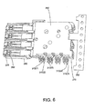
- FIG. 6 shows the daughter card connector during assembly. Wafers 260 and 270 have been attached. Also, alignment guide 250 have been inserted and secured to the wafers. Portions of carrier strip 352 remain for ease of handling and can be removed at a subsequent step of manufacture.
- FIG. 6 shows the mating portions 262 of the contacts under lip 259.
- the mating portions 262 and 272 are pressed toward wall 256 of alignment guide 250 so that they will slide under lip 259.
- FIG. 6 also illustrates the spacing between contact tails to facilitate use of the power connector in a backplane assembly including the signal wafers shown in FIG. 1 .
- each of the power contacts has two contact tails, such as 312(1) and 312(2). These contact tails are on the same pitch as the signal contact tails of the signal connector of FIG. 1 .
- the distance between the centers of contact tails 312(1) and 312(2) represents the spacing along a column of contacts.
- the signal contacts are disposed in pairs. And, the spacing between the tails of one pair and closest tail in an adjacent pair is greater than the spacing between contact tails in the same pair. In the preferred embodiment, the power connector of the invention has this same spacing.
- the distance between the centers of tails 312(2) and 312(5) matches the distance between the pairs of signal contact tails shown in FIG. 1 .
- the pitch of signal contacts within a row is the same for all power contact tails. In FIG. 6 , this spacing is given by the distance between the center lines of tails 312(3) and 312(4).
- the power connector subassembly containing wafers 260 and 270 might be wider than two signal wafers as shown in FIG. 1 , the power connector subassembly preferably has a width that is an integer multiple of the width of a signal contact wafer. This width allows the signal and power contacts to be easily mounted to a support member, such as a metal stiffener that has preformed attachment features for the wafers.
- the spacing between tails in a row is shown as the distance between tails 312(3) and 312(4) and that distance is twice the distance as the spacing between adjacent columns of signal contact tails.
- the power connector can be used to carry up to eight individual power signals. Alternatively, certain power contacts can be electrically connected together.
- a power connector as described above has several advantages. First, it is easy to manufacture. Secondly, it is compatible with signal connection systems. It can fit on the same stiffener as the signal connectors. Further, it takes up only a little space. In the illustrated embodiment it takes up less than the space of three columns of signal contacts. Being able to fit eight separate power contacts in such a small space is very advantageous.
- the power connector according to the design is very flexible to achieve greater power capacity utilization.
- Such a connector has more power contacts than prior art power connectors, though in the preferred embodiment each has a lower current rating.
- a prior art power connector has four large power contacts, each rated to carry 10Amps, for a total of 40 Amps max.
- the power connector of the invention uses stock 12 mils thick to make power contact blank 300. Each such contact carries 5Amps, but for a total of 40 Amps max.
- each power connector has the same maximum power carrying capacity, the connector of the invention can be more efficient, particularly in a system when many voltage levels are required.
- one contact can carry each of the 1V, 0V and 2.5V signals.
- Three contacts are needed to carry the 5V signal at 15Amps. But, because there are 8 contacts in one connector, all signals can be carried in one power connector. The result is a 60% power capacity utilization and a much smaller area needed for power connectors because one, rather than two power connectors are needed.
- the disclosed power connector is narrower than the prior art connector with 4 large blades.
- the intermediate portions 301...304 of the power contacts are generally in a plane and that this plane will be parallel to the plane of the signal contacts.
- the power conductors are generally running beside and parallel to the signal contacts. This configuration minimizes the inductance in the conductive loop that is formed by current flowing on and off the daughter card and is highly desirable for high speed interconnection systems.
- the connector is described as a right angle backplane connector.
- Connectors might also be used in a mezzanine or mother board application or in a cable configuration or in other ways, such as a midplane.
- These alternative embodiments can be created by changing the manner of attachment of the connector to a particular substrate.
- press fit contacts are shown in the illustrated embodiment for attachment to a printed circuit boards.
- the specific attachment mechanism could be changed by changing the contact tails. Solder tails or other attachment mechanisms could be used.
- the blades 214 could be made of different lengths so that certain power contacts will mate first as the daughter card and backplane connectors are pressed together.
- the preferred embodiment is a power connector that is the width of three signal wafers.
- thicker stock might be used to provide contacts of 10Amps each.
- the power connector might be wider, such as the width of 4 signal wafers. Because the power connectors, if made an integer multiple of signal wafers easily fit on the same stiffener, the larger power connectors might be used instead of or in addition to smaller ones.
- the shape of the power contacts shown in FIG. 3 is illustrative. It would be desirable to make the intermediate portions 301...304 as wide as possible to reduce their impedance. Also, it might be desirable to make the power contacts as short as possible to reduce the inductance. Thus, the intermediate portions might be made without the sharp corners shown in intermediate portions 301...303 and might curve through a right angle with more of a smooth curve as shown in intermediate portions 304.
- the tie bars 350 are severed before the power connector is used.
- power contacts will often be commoned together. Where power contacts are commoned, it might be desirable to leave the tie bars 350 joining the power contacts, because this would better balance the power flow.
- the blades of the backplane connector could also be electrically connected inside the connector. For example, a U-shaped structure could be made in place of two blades.
- the preferred embodiment shows the daughter card connector with mating contact portions 262 and 272 that are beams to provide spring force against the mating contact in the backplane connector.
- the mating contact is simply a flat blade. It would be possible to provide daughter card contacts that are blades and mating contacts in the backplane portion of the connector that include beams that generate spring force.
Landscapes
- Coupling Device And Connection With Printed Circuit (AREA)
- Connector Housings Or Holding Contact Members (AREA)
- Details Of Connecting Devices For Male And Female Coupling (AREA)
Abstract
Description
- This invention relates generally to electrical interconnect systems and more particularly to power connectors.
- Modem electronic systems are often built on multiple printed circuit boards. A traditional configuration for a computerized product, such as a router, is to have a printed circuit board that serves as a backplane. Several other printed circuit boards, called daughter cards, are connected to the backplane. The daughter cards contain the electronic circuitry of the system. The backplane contains traces or planes that route signal and power to the daughter cards. Electrical connectors are attached to the printed circuit boards and electrical connections are made through these connectors.
- Different types of connectors are generally used for signals and power connections. Signal connectors should carry many signals in a small area. However, because the signals are often of high frequency, there is a risk of cross-talk. Therefore, the signal connectors often have special shielding.
- Power connectors need to carry much higher current than signal connectors. In addition, because the power in an electronic system might have a dangerous voltage, the backplane power connectors often need protective features to prevent a human from accidentally contacting a power conductor. Thus, many of the requirements for signal and power connectors are different.
- One requirement of power connectors that does not exist with signal connectors is the need for various mating levels. The mating levels are particularly useful for a function called "hot swap". With hot swap, a connection is made or removed while system power is on. For example, a daughter card might be plugged into a backplane while the power is on. To ensure proper operation of the circuitry on the daughter card, or to avoid damage to the daughter card circuitry, it is often desirable that power be applied to various components in a particular order. Multiple mating levels are used to provide this capability.
- The circuits that are to receive power first are connected to the longest power contacts. These contacts mate first and therefore provide power to selected circuits first. As electronic systems get more complicated, the number of mating levels required increases.
- Also, as systems get more complicated, the circuitry requires more voltage levels to operate correctly.
- It would be desirable to have a power connector that could flexibly handle many voltage levels and mating levels.
- Further, we have recognized that for high speed interconnects, it is desirable to have a low inductance power power/return loop.
-
US Patent 5993259 andWO 98/35409 Figure 1 . The connector has intermateable first and second pieces, the first piece being a pin header in an insulative housing, and the second piece being a daughter card connector with plural stacked wafers, each wafer having a housing over a shield to form a shield piece and also a signal piece which connects to the shield piece. -
US Patent 5295843 discloses an electrical connector in which at least one conductive power contact has a pair of conductive fingers for radiating heat. - The invention provides a power connector as defined in
Claim 1. - The preferred connector is assembled from two different types of wafers and with an insulative cap, the connector mating with a backplane power module having enclosed contacts.
- The invention will be better understood by reference to the following more detailed description and accompanying drawings in which
-
FIG. 1 shows in exploded view a signal connector for use with the invention; -
FIG. 2 shows an exploded view of a power connector made according to a preferred embodiment of the invention; -
FIG. 3 is a sketch of contact blank used to make a wafer of the connector inFIG. 2 ; -
FIG. 4 is a sketch of a first wafer shown inFIG. 2 ; -
FIG. 5 is sketch of a second wafer shown inFIG. 2 ; -
FIG. 6 is a sketch of a daughter card power connector according to the invention. -
FIG. 1 shows a signal connector portion of a high speed interconnect system. A portion of abackplane 104 is shown and abackplane connector 110 is attached to it. A portion of adaughter card 102 is also shown, adaughter card connector 120 is shown in exploded view. The daughter card connector is assembled from a plurality ofsubassemblies 136. Thesubassemblies 136 are attached to astiffener 142 that has attachment features, such asholes slots 162c that both position and secure the subassemblies. -
FIG. 2 shows a preferred embodiment of apower connector 200 according to the invention.Power connector 200 is intended to operate in conjunction with signal connectors, such as are shown inFIG. 1 and more fully described in provisionalUS Patent Application 60/179,722 power connector 200 will attach to stiffener 142 along side the signal connectors and the backplane portions ofpower connector 200 will attach tobackplane 104 alongside backplane connectors 110. -
FIG. 2 showsconnector 200 in exploded view. A backplane connector contains anhousing 210 andseveral power contacts 212.Housing 210 is preferably made of an insulative material. In the preferred embodiment,housing 210 is formed by molding, more preferably by injection molding. - The
power contacts 212 are made of a conducting material. Copper alloys are often used for power contacts, but other high conductivity metals with suitable stiffness might be used. Eachpower contact 212 has ablade 214 and a plurality ofcontact tails 216. In the illustrated embodiment, two press fit contact tails are shown. In use, the press fit contact tails are pressed into plated through holes in a backplane to make contact to the power plane within the backplane. - In the embodiment of
FIG.2 , there are eightpower contacts 212 insidehousing 210. Thepower contacts 212 are pressed through openings (not shown) in the floor of thehousing 210. Eachblade 214 runs up agroove 218 formed in the wall ofhousing 210. In the illustrated embodiment, theblades 214 line opposing walls ofhousing 210 leaving acavity 220 between them. The specific number of blades in the backplane connector is not important to the invention. However, thebackplane housing 210 preferably has the same width or smaller than thesignal connector shroud 110 so that both signal connectors and power connectors may fit in a line. -
Housing 210 is also formed withgrooves 222.Grooves 222 receiveprojections 252 from the daughter card connector during mating of the daughter card and backplane connectors.Grooves 222 are alignment features that ensure the power contacts are properly aligned. - The daughter card connector is assembled from three components, a cap or
alignment guide 250, awafer 260 and awafer 270.Wafers wafers mating portions - Each of the
wafers FIG. 3 ). Preferably, the housing is formed of an insulative material, such as plastic. The housings contain attachment features, such asprojections stiffener 142. Attachment features can be such things as tabs that slide into grooves or hubs that press through holes. - The
housings FIG. 2 ,projections 278 extend from the inner surface ofwafer 270.Projections 278 fit in holes on the inner surface (not shown) ofwafer 260 to align the wafers.Projections 278 also create an interference fit to holdwafers - Contact
tails wafers tails contact tails 146 in the daughtercard signal connector 120. Using the same spacing provides an advantage of allowing a uniform hole pattern across the printed circuit board, which can sometimes simplify manufacture, particularly the layout stage of the PCB design. - Contact
portions blade 214. As shown, each beam has a curved portion and adimple 291 formed therein.Dimples 291 aid in making contact toblades 214 in the backplane connector. - The contact portions are inserted into the
alignment guide 250. The alignment guide is formed from an insulative material to prevent the contacts from shorting together. Preferably, it is molded from plastic.Alignment guide 250 contains a plurality ofchannels 254 formed therein. Eachchannel 254 receives one of thecontacts Alignment guide 250 haswalls channels 254. - Each of the
channels 254 has alip 250 formed near the mating edge ofalignment guide 250. When assembled, the front edge of thecontacts lip 259. Preferably, thecontacts Lip 250 will keep the leading edge of the contacts within the outline of the daughter card connector so that they can be inserted intocavity 220 without stubbing. However, the contacts will be pre-loaded to press outward against and will increase the force with which thedimples 291 press againstblades 214, thereby improving the integrity of the contact. - To secure the
alignment guide 250 to thewafers 260 and 20, each of the signal contacts containsbarbs 269. When thealignment guide 250 is pressed onto the wafers,barbs 269 will engage features onwalls 258 thereby securing the alignment guide to the wafers. Other methods of attachment could be used. For example, features could be molded into thealignment guide 250 and thehousings -
FIG. 3 shows awafer 270 at an early stage of manufacture. A power contact blank 300 is shown. This blank is stamped and formed from the material used to make the power contacts. In the preferred embodiment, a copper alloy is used. Preferably, numerous such blanks are stamped from a single large sheet of metal that can be rolled up for easy handling. The blank 300 is stamped with the desired number of power contacts, herepower contacts mating portion 272 and contacttails 312. In the illustrated embodiment, each of thecontacts 301...304 has acontact tail 312 with two press fit contacts. Using multiple contacts increases the power carrying capacity while keeping the holes in the daughter card that receive the tails on a pitch that matches the pitch for the signal contact holes. - Each of the
power contacts 301...304 has an intermediate portion that connects thetails 312 to thecontacts 272. - The individual contacts are held together by tie bars 350. The tie bars are severed to create electrically separate contacts. Preferably, the tie bars are separated after
housing 273 is molded. Thecontact blank 300 is also held on carrier strips 352. These carrier strips are also severed after molding when no longer needed. In a preferred embodiment, the carrier strips contain holes that are used for positioning the contacts, which are not severed until no longer needed. -
FIG. 3 shows that thecontacts 301...304 have ajog 314 formed therein.Jog 314 takes thecontact tails 312 away from the center of the daughter card connector.Jog 314 increases the spacing between thecontact tails 312 in thewafers jog 314 were omitted. Providing greater separation between holes in printed circuit boards that carry relatively high voltage is desirable. - In addition, jogs 314 bring the
contact tails 312 in line with holes that are spaced the same pitch as the holes along the rows used to mount the signal connectors. In the illustrated embodiment, the power connector is as wide as the wafers needed to carry three columns of signal contacts. Thus, jogs 314 make the spacing between thetails 312 inwafers signal wafers 136. - Turning now to
FIG. 4 , the power contact blank is shown in a later stage of manufacture. Thehousing 273 is molded over thepower contact blank 300.FIG. 4 shows thewafer 270 before carrier strips 352 and tiebars 350 are severed. -
Wafer 260 is formed through a similar process. A complementary power contact blank is used. In particular, themating portions 272 have an opposite curve and thejogs 314 are in the opposite direction. In both wafers, though, these portions bend away from the center of the daughter card connector.FIG. 5 showswafer 260 afterhousing 263 has been molded over the power contact blank. -
FIG. 6 shows the daughter card connector during assembly.Wafers alignment guide 250 have been inserted and secured to the wafers. Portions ofcarrier strip 352 remain for ease of handling and can be removed at a subsequent step of manufacture. -
FIG. 6 shows themating portions 262 of the contacts underlip 259. To assemble the daughter card connector, themating portions wall 256 ofalignment guide 250 so that they will slide underlip 259. -
FIG. 6 also illustrates the spacing between contact tails to facilitate use of the power connector in a backplane assembly including the signal wafers shown inFIG. 1 . As shown inFIG. 6 , each of the power contacts has two contact tails, such as 312(1) and 312(2). These contact tails are on the same pitch as the signal contact tails of the signal connector ofFIG. 1 . The distance between the centers of contact tails 312(1) and 312(2) represents the spacing along a column of contacts. - In the signal connector optimized for handling differential signals, the signal contacts are disposed in pairs. And, the spacing between the tails of one pair and closest tail in an adjacent pair is greater than the spacing between contact tails in the same pair. In the preferred embodiment, the power connector of the invention has this same spacing. The distance between the centers of tails 312(2) and 312(5) matches the distance between the pairs of signal contact tails shown in
FIG. 1 . - The pitch of signal contacts within a row is the same for all power contact tails. In
FIG. 6 , this spacing is given by the distance between the center lines of tails 312(3) and 312(4). Though the power connectorsubassembly containing wafers FIG. 1 , the power connector subassembly preferably has a width that is an integer multiple of the width of a signal contact wafer. This width allows the signal and power contacts to be easily mounted to a support member, such as a metal stiffener that has preformed attachment features for the wafers. It also allows holes in the printed circuit board for attachment of the connectors to be drilled in a pattern that has uniform pitch - though where a power connector is used, a column of holes might be unused or not drilled. Or, the holes used for the power connector attachment are likely to be of larger diameter to carry more current. In the illustrated embodiment, the spacing between tails in a row is shown as the distance between tails 312(3) and 312(4) and that distance is twice the distance as the spacing between adjacent columns of signal contact tails. - In use, the power connector can be used to carry up to eight individual power signals. Alternatively, certain power contacts can be electrically connected together.
- A power connector as described above has several advantages. First, it is easy to manufacture. Secondly, it is compatible with signal connection systems. It can fit on the same stiffener as the signal connectors. Further, it takes up only a little space. In the illustrated embodiment it takes up less than the space of three columns of signal contacts. Being able to fit eight separate power contacts in such a small space is very advantageous.
- Another advantage is that the power connector according to the design is very flexible to achieve greater power capacity utilization. Such a connector has more power contacts than prior art power connectors, though in the preferred embodiment each has a lower current rating. For example, a prior art power connector has four large power contacts, each rated to carry 10Amps, for a total of 40 Amps max. In one embodiment, the power connector of the invention uses stock 12 mils thick to make
power contact blank 300. Each such contact carries 5Amps, but for a total of 40 Amps max. Though each power connector has the same maximum power carrying capacity, the connector of the invention can be more efficient, particularly in a system when many voltage levels are required. - For example, consider a system in which four voltage levels are need: one at 1V and 2 Amps, one at 0V and 5A, one at 2.5V and 2 Amps and one at 5V and 15 Amps. In the prior art power connector, one 10 Amp contact can carry voltages at 1V, 0V and 2.5V because each has a current below the 10A level. However, two contacts are needed to carry all 15 Amps at 5V. Thus, a total of 5 contacts are needed. Because each connector has four contacts, two power connectors are needed. Of the total current carrying capacity of 80 Amps in the two power connectors only 24 Amps is carried in this example. In other words, only a 30% power capacity utilization is achieved.
- With a connector as in the preferred embodiment, one contact can carry each of the 1V, 0V and 2.5V signals. Three contacts are needed to carry the 5V signal at 15Amps. But, because there are 8 contacts in one connector, all signals can be carried in one power connector. The result is a 60% power capacity utilization and a much smaller area needed for power connectors because one, rather than two power connectors are needed.
- And, in the preferred embodiment, the disclosed power connector is narrower than the prior art connector with 4 large blades.
- Further, it should be noted that the
intermediate portions 301...304 of the power contacts are generally in a plane and that this plane will be parallel to the plane of the signal contacts. As a result, the power conductors are generally running beside and parallel to the signal contacts. This configuration minimizes the inductance in the conductive loop that is formed by current flowing on and off the daughter card and is highly desirable for high speed interconnection systems. - Having described one embodiment, numerous alternative embodiments or variations might be made. For example, the connector is described as a right angle backplane connector. Connectors might also be used in a mezzanine or mother board application or in a cable configuration or in other ways, such as a midplane. These alternative embodiments can be created by changing the manner of attachment of the connector to a particular substrate. Likewise, press fit contacts are shown in the illustrated embodiment for attachment to a printed circuit boards. Even for connectors used in a backplane configuration, the specific attachment mechanism could be changed by changing the contact tails. Solder tails or other attachment mechanisms could be used.
- Also, it is sometimes desirable to have a predefined mating sequence for power connectors. The
blades 214 could be made of different lengths so that certain power contacts will mate first as the daughter card and backplane connectors are pressed together. - It should also be noted that the preferred embodiment is a power connector that is the width of three signal wafers. However, it would be possible to use thicker stock to make the power contacts and achieve higher current capacities. For example, 25 mil stock might be used to provide contacts of 10Amps each. With such a configuration, the power connector might be wider, such as the width of 4 signal wafers. Because the power connectors, if made an integer multiple of signal wafers easily fit on the same stiffener, the larger power connectors might be used instead of or in addition to smaller ones.
- Also, it should be appreciated that the shape of the power contacts shown in
FIG. 3 is illustrative. It would be desirable to make theintermediate portions 301...304 as wide as possible to reduce their impedance. Also, it might be desirable to make the power contacts as short as possible to reduce the inductance. Thus, the intermediate portions might be made without the sharp corners shown inintermediate portions 301...303 and might curve through a right angle with more of a smooth curve as shown inintermediate portions 304. - As another variation, it was indicated above that the tie bars 350 are severed before the power connector is used. However, when large current carrying capacity is required, power contacts will often be commoned together. Where power contacts are commoned, it might be desirable to leave the tie bars 350 joining the power contacts, because this would better balance the power flow. As yet another embodiment, the blades of the backplane connector could also be electrically connected inside the connector. For example, a U-shaped structure could be made in place of two blades.
- Further, it is described that holes in the printed circuit board on the same pitch as the holes used to make connection top the signal contacts. The placement of the holes for the power connector can follow any pattern
- As a further variation, it would be possible to change the shape of the contacts. For example, the preferred embodiment shows the daughter card connector with
mating contact portions - Therefore, the invention should be limited only by the scope of the appended claims.
Claims (13)
- A power connector (200) having an intermateable first piece and second piece, the first piece comprising:a) an insulative housing (210) having a central cavity (220);b) a plurality of blades (214) at the periphery of the central cavity (220); andthe second connector piece comprising:a) a first wafer (260) having power contacts (301-304) running therethrough, the wafer (260) having a front edge and the power contacts having mating portions (262) extending from the front edge of the wafer;b) a second wafer (270), attached to the first wafer (260), having power contacts (301-304) running therethrough, the wafer (270) having a front edge and the power contacts having mating portions (272) extending from the front edge of the wafer;c) a cap (250) attached to the first wafer (260) and the second wafer (270) having an insulative wall (256) disposed between the mating portions (262, 272) of the power contacts of the first wafer and the second wafer;wherein the power contacts in the second connector piece are aligned with the blades in the first connector piece when the first and second connector pieces are mated.
- The power connector (200) of claim 1, wherein the housing (210) of the first piece has opposing side walls with channels (218) formed therein and the blades are disposed in channels of the side wall.
- The power connector (200) of claim 1, wherein the power contacts of the second connector piece comprise dual beam contacts (262, 272).
- The power connector (200) of claim 1, wherein the first wafer (260) and the second wafer (270) have attachment features (278) thereon, thereby attaching the first wafer to the second wafer.
- The power connector (200) of claim 1, wherein power contacts of the second connector piece have features (269) formed thereon, said features engaging the cap (250), thereby attaching the cap to the first and second wafers.
- The power connector (200) of claim 1, wherein the power contacts (301-304) of the second connector piece traverse a right angle.
- The power connector (200) of claim 1, wherein the cap (250) additionally has a plurality of insulative walls (258) between adjacent power contacts on each of the first and second wafer.
- The power connector (200) of claim 1, wherein the cap (250) has a front edge with a plurality of lips (259) along the front edge and the tips of the mating portions (262, 272) of the power contacts are under respective ones of the lips.
- The power connector (200) of claim 8, wherein the housing (210) of the first piece has opposing side walls with channels (218) formed therein and the blades are disposed in channels of the side wail.
- The power connector (200) of claim 9, wherein power contacts of the second connector piece have features (269) formed thereon, said features engaging the cap (250), thereby attaching the cap to the first and second wafers.
- The power connector (200) of claim 1, wherein the second connector piece further comprises a plurality of signal wafers (136).
- The power connector (200) of claim 11, wherein the second connector piece further comprises a support member (142) having points of attachment (162a-c) for wafers spaced on a predetermined pitch, the signal wafers and the first and second wafers being attached to the points of attachment.
- The power connector (200) of claim 11, wherein the signal wafers (136) include differential signal wafers each having a plurality of pairs of contact tails (146) with the spacing between the contact tails being a first distance and the spacing between the contacts in different pairs being a second, larger distance, and wherein the first and second wafers include a plurality of contact tails (312A, 312B) aligned with the contact tails (146) of the differential signal wafers.
Applications Claiming Priority (3)
| Application Number | Priority Date | Filing Date | Title |
|---|---|---|---|
| US769867 | 2001-01-25 | ||
| US09/769,867 US6592381B2 (en) | 2001-01-25 | 2001-01-25 | Waferized power connector |
| PCT/US2002/001886 WO2002060013A1 (en) | 2001-01-25 | 2002-01-23 | Waferized power connector |
Publications (2)
| Publication Number | Publication Date |
|---|---|
| EP1356547A1 EP1356547A1 (en) | 2003-10-29 |
| EP1356547B1 true EP1356547B1 (en) | 2011-01-05 |
Family
ID=25086749
Family Applications (1)
| Application Number | Title | Priority Date | Filing Date |
|---|---|---|---|
| EP02705906A Expired - Lifetime EP1356547B1 (en) | 2001-01-25 | 2002-01-23 | Waferized power connector |
Country Status (9)
| Country | Link |
|---|---|
| US (1) | US6592381B2 (en) |
| EP (1) | EP1356547B1 (en) |
| JP (1) | JP4041400B2 (en) |
| CN (1) | CN1316682C (en) |
| CA (1) | CA2436064A1 (en) |
| DE (1) | DE60238817D1 (en) |
| MX (1) | MXPA03006691A (en) |
| TW (1) | TW578337B (en) |
| WO (1) | WO2002060013A1 (en) |
Families Citing this family (110)
| Publication number | Priority date | Publication date | Assignee | Title |
|---|---|---|---|---|
| DE50210105D1 (en) * | 2001-07-30 | 2007-06-21 | Harting Electronics Gmbh & Co | Electrical connector |
| US6638079B1 (en) * | 2002-05-21 | 2003-10-28 | Hon Hai Precision Ind. Co., Ltd. | Customizable electrical connector |
| US20040147169A1 (en) | 2003-01-28 | 2004-07-29 | Allison Jeffrey W. | Power connector with safety feature |
| DE10310502A1 (en) * | 2003-03-11 | 2004-09-23 | Molex Inc., Lisle | Earthed electrical connector for GHz signal frequency range, has earthing terminal provided with at least 2 mechanically coupled electrical contacts |
| US6884117B2 (en) * | 2003-08-29 | 2005-04-26 | Hon Hai Precision Ind. Co., Ltd. | Electrical connector having circuit board modules positioned between metal stiffener and a housing |
| US7074086B2 (en) * | 2003-09-03 | 2006-07-11 | Amphenol Corporation | High speed, high density electrical connector |
| US6894516B1 (en) * | 2003-11-20 | 2005-05-17 | International Business Machines Corporation | Method and apparatus for implementing very high density probing (VHDP) of printed circuit board signals |
| WO2005065254A2 (en) | 2003-12-31 | 2005-07-21 | Fci Americas Technology, Inc. | Electrical power contacts and connectors comprising same |
| US7458839B2 (en) | 2006-02-21 | 2008-12-02 | Fci Americas Technology, Inc. | Electrical connectors having power contacts with alignment and/or restraining features |
| US7182642B2 (en) * | 2004-08-16 | 2007-02-27 | Fci Americas Technology, Inc. | Power contact having current flow guiding feature and electrical connector containing same |
| US7175445B2 (en) * | 2004-08-31 | 2007-02-13 | Tyco Electronics Corporation | Electrical connector power wafers |
| US7359214B2 (en) * | 2004-09-28 | 2008-04-15 | Amphenol Corporation | Backplane with routing to reduce layer count |
| US7281950B2 (en) * | 2004-09-29 | 2007-10-16 | Fci Americas Technology, Inc. | High speed connectors that minimize signal skew and crosstalk |
| US20060073709A1 (en) * | 2004-10-06 | 2006-04-06 | Teradyne, Inc. | High density midplane |
| US7476108B2 (en) | 2004-12-22 | 2009-01-13 | Fci Americas Technology, Inc. | Electrical power connectors with cooling features |
| US7384289B2 (en) | 2005-01-31 | 2008-06-10 | Fci Americas Technology, Inc. | Surface-mount connector |
| US7303427B2 (en) | 2005-04-05 | 2007-12-04 | Fci Americas Technology, Inc. | Electrical connector with air-circulation features |
| US7303401B2 (en) * | 2005-06-23 | 2007-12-04 | Fci Americas Technology, Inc. | Electrical connector system with header connector capable of direct and indirect mounting |
| US20090291593A1 (en) | 2005-06-30 | 2009-11-26 | Prescott Atkinson | High frequency broadside-coupled electrical connector |
| US7163421B1 (en) * | 2005-06-30 | 2007-01-16 | Amphenol Corporation | High speed high density electrical connector |
| US7326082B2 (en) * | 2005-11-21 | 2008-02-05 | Tyco Electronics Corporation | Electrical connector |
| US7431616B2 (en) * | 2006-03-03 | 2008-10-07 | Fci Americas Technology, Inc. | Orthogonal electrical connectors |
| US20070207632A1 (en) * | 2006-03-03 | 2007-09-06 | Fci Americas Technology, Inc. | Midplane with offset connectors |
| US7407413B2 (en) * | 2006-03-03 | 2008-08-05 | Fci Americas Technology, Inc. | Broadside-to-edge-coupling connector system |
| DE102006011624A1 (en) * | 2006-03-10 | 2007-09-13 | Carl Zeiss Meditec Ag | Device and method for the defined alignment of an eye |
| US7425145B2 (en) | 2006-05-26 | 2008-09-16 | Fci Americas Technology, Inc. | Connectors and contacts for transmitting electrical power |
| US7726982B2 (en) | 2006-06-15 | 2010-06-01 | Fci Americas Technology, Inc. | Electrical connectors with air-circulation features |
| US7500871B2 (en) | 2006-08-21 | 2009-03-10 | Fci Americas Technology, Inc. | Electrical connector system with jogged contact tails |
| JP2008146888A (en) * | 2006-12-07 | 2008-06-26 | Hirose Electric Co Ltd | Electrical connector |
| US7503804B2 (en) * | 2006-12-19 | 2009-03-17 | Fci Americas Technology Inc. | Backplane connector |
| US7497736B2 (en) | 2006-12-19 | 2009-03-03 | Fci Americas Technology, Inc. | Shieldless, high-speed, low-cross-talk electrical connector |
| US7422444B1 (en) * | 2007-02-28 | 2008-09-09 | Fci Americas Technology, Inc. | Orthogonal header |
| WO2008124101A2 (en) * | 2007-04-04 | 2008-10-16 | Amphenol Corporation | Electrical connector lead frame |
| US7794240B2 (en) * | 2007-04-04 | 2010-09-14 | Amphenol Corporation | Electrical connector with complementary conductive elements |
| US7722401B2 (en) | 2007-04-04 | 2010-05-25 | Amphenol Corporation | Differential electrical connector with skew control |
| US7641500B2 (en) | 2007-04-04 | 2010-01-05 | Fci Americas Technology, Inc. | Power cable connector system |
| TWM322090U (en) * | 2007-05-11 | 2007-11-11 | Chief Land Electronic Co Ltd | Ground terminal capable of preventing noise |
| US7905731B2 (en) | 2007-05-21 | 2011-03-15 | Fci Americas Technology, Inc. | Electrical connector with stress-distribution features |
| US7811100B2 (en) | 2007-07-13 | 2010-10-12 | Fci Americas Technology, Inc. | Electrical connector system having a continuous ground at the mating interface thereof |
| US7762857B2 (en) | 2007-10-01 | 2010-07-27 | Fci Americas Technology, Inc. | Power connectors with contact-retention features |
| US7682193B2 (en) * | 2007-10-30 | 2010-03-23 | Fci Americas Technology, Inc. | Retention member |
| EP2240980A2 (en) | 2008-01-17 | 2010-10-20 | Amphenol Corporation | Electrical connector assembly |
| US8764464B2 (en) | 2008-02-29 | 2014-07-01 | Fci Americas Technology Llc | Cross talk reduction for high speed electrical connectors |
| US7748997B2 (en) * | 2008-07-22 | 2010-07-06 | Tyco Electronics Corporation | Receptacle for electrical connectors |
| US8062051B2 (en) | 2008-07-29 | 2011-11-22 | Fci Americas Technology Llc | Electrical communication system having latching and strain relief features |
| US8771023B2 (en) * | 2008-09-30 | 2014-07-08 | Fci | Lead frame assembly for an electrical connector |
| US8083547B2 (en) * | 2008-10-01 | 2011-12-27 | Amphenol Corporation | High density pluggable electrical and optical connector |
| US8298015B2 (en) | 2008-10-10 | 2012-10-30 | Amphenol Corporation | Electrical connector assembly with improved shield and shield coupling |
| US8545240B2 (en) | 2008-11-14 | 2013-10-01 | Molex Incorporated | Connector with terminals forming differential pairs |
| MY155071A (en) | 2008-12-12 | 2015-08-28 | Molex Inc | Resonance modifying connector |
| USD610548S1 (en) | 2009-01-16 | 2010-02-23 | Fci Americas Technology, Inc. | Right-angle electrical connector |
| USD606496S1 (en) | 2009-01-16 | 2009-12-22 | Fci Americas Technology, Inc. | Right-angle electrical connector |
| USD664096S1 (en) | 2009-01-16 | 2012-07-24 | Fci Americas Technology Llc | Vertical electrical connector |
| USD606497S1 (en) | 2009-01-16 | 2009-12-22 | Fci Americas Technology, Inc. | Vertical electrical connector |
| USD608293S1 (en) | 2009-01-16 | 2010-01-19 | Fci Americas Technology, Inc. | Vertical electrical connector |
| USD640637S1 (en) | 2009-01-16 | 2011-06-28 | Fci Americas Technology Llc | Vertical electrical connector |
| USD619099S1 (en) | 2009-01-30 | 2010-07-06 | Fci Americas Technology, Inc. | Electrical connector |
| US8323049B2 (en) | 2009-01-30 | 2012-12-04 | Fci Americas Technology Llc | Electrical connector having power contacts |
| US8172614B2 (en) | 2009-02-04 | 2012-05-08 | Amphenol Corporation | Differential electrical connector with improved skew control |
| CN102405564B (en) * | 2009-02-18 | 2014-09-03 | 莫列斯公司 | Vertical Connectors for Printed Circuit Boards |
| US9277649B2 (en) | 2009-02-26 | 2016-03-01 | Fci Americas Technology Llc | Cross talk reduction for high-speed electrical connectors |
| US8366485B2 (en) | 2009-03-19 | 2013-02-05 | Fci Americas Technology Llc | Electrical connector having ribbed ground plate |
| USD618180S1 (en) | 2009-04-03 | 2010-06-22 | Fci Americas Technology, Inc. | Asymmetrical electrical connector |
| USD618181S1 (en) | 2009-04-03 | 2010-06-22 | Fci Americas Technology, Inc. | Asymmetrical electrical connector |
| US8834204B2 (en) * | 2009-06-04 | 2014-09-16 | Fci | Connector assembly |
| CN102598430B (en) | 2009-09-09 | 2015-08-12 | 安费诺有限公司 | For the compression contacts of high-speed electrical connectors |
| US8267721B2 (en) | 2009-10-28 | 2012-09-18 | Fci Americas Technology Llc | Electrical connector having ground plates and ground coupling bar |
| US8616919B2 (en) * | 2009-11-13 | 2013-12-31 | Fci Americas Technology Llc | Attachment system for electrical connector |
| WO2011140438A2 (en) | 2010-05-07 | 2011-11-10 | Amphenol Corporation | High performance cable connector |
| US8657627B2 (en) | 2011-02-02 | 2014-02-25 | Amphenol Corporation | Mezzanine connector |
| US8961227B2 (en) | 2011-02-07 | 2015-02-24 | Amphenol Corporation | Connector having improved contacts |
| US8814595B2 (en) * | 2011-02-18 | 2014-08-26 | Amphenol Corporation | High speed, high density electrical connector |
| US8262412B1 (en) | 2011-05-10 | 2012-09-11 | Tyco Electronics Corporation | Electrical connector having compensation for air pockets |
| EP2624034A1 (en) | 2012-01-31 | 2013-08-07 | Fci | Dismountable optical coupling device |
| CN103296510B (en) | 2012-02-22 | 2015-11-25 | 富士康(昆山)电脑接插件有限公司 | The manufacture method of terminal module and terminal module |
| US9257778B2 (en) | 2012-04-13 | 2016-02-09 | Fci Americas Technology | High speed electrical connector |
| US8944831B2 (en) | 2012-04-13 | 2015-02-03 | Fci Americas Technology Llc | Electrical connector having ribbed ground plate with engagement members |
| USD727852S1 (en) | 2012-04-13 | 2015-04-28 | Fci Americas Technology Llc | Ground shield for a right angle electrical connector |
| USD718253S1 (en) | 2012-04-13 | 2014-11-25 | Fci Americas Technology Llc | Electrical cable connector |
| USD727268S1 (en) | 2012-04-13 | 2015-04-21 | Fci Americas Technology Llc | Vertical electrical connector |
| USD751507S1 (en) | 2012-07-11 | 2016-03-15 | Fci Americas Technology Llc | Electrical connector |
| US9543703B2 (en) | 2012-07-11 | 2017-01-10 | Fci Americas Technology Llc | Electrical connector with reduced stack height |
| CN104704682B (en) | 2012-08-22 | 2017-03-22 | 安费诺有限公司 | High-frequency electrical connector |
| CN103730745B (en) * | 2012-10-16 | 2016-02-03 | 欧品电子(昆山)有限公司 | Electric connector and combination thereof |
| USD745852S1 (en) | 2013-01-25 | 2015-12-22 | Fci Americas Technology Llc | Electrical connector |
| USD720698S1 (en) | 2013-03-15 | 2015-01-06 | Fci Americas Technology Llc | Electrical cable connector |
| US9362693B2 (en) * | 2014-01-14 | 2016-06-07 | Tyco Electronics Corporation | Header assembly having power and signal cartridges |
| WO2015112717A1 (en) | 2014-01-22 | 2015-07-30 | Amphenol Corporation | High speed, high density electrical connector with shielded signal paths |
| CN104882703B (en) * | 2014-02-28 | 2017-09-05 | 凡甲电子(苏州)有限公司 | Electric connector |
| JP6251624B2 (en) * | 2014-03-31 | 2017-12-20 | 株式会社エンプラス | Contact pin unit and socket for electrical parts using the same |
| US9362638B2 (en) * | 2014-09-03 | 2016-06-07 | Amphenol Corporation | Overmolded contact wafer and connector |
| US10541482B2 (en) | 2015-07-07 | 2020-01-21 | Amphenol Fci Asia Pte. Ltd. | Electrical connector with cavity between terminals |
| TWI790798B (en) | 2016-08-23 | 2023-01-21 | 美商安芬諾股份有限公司 | Connector configurable for high performance |
| CN118630506A (en) | 2017-10-30 | 2024-09-10 | 安费诺富加宜(亚洲)私人有限公司 | Low Crosstalk Card Edge Connectors |
| US10665973B2 (en) * | 2018-03-22 | 2020-05-26 | Amphenol Corporation | High density electrical connector |
| CN208862209U (en) | 2018-09-26 | 2019-05-14 | 安费诺东亚电子科技(深圳)有限公司 | A kind of connector and its pcb board of application |
| WO2020073460A1 (en) | 2018-10-09 | 2020-04-16 | Amphenol Commercial Products (Chengdu) Co. Ltd. | High-density edge connector |
| US11381015B2 (en) | 2018-12-21 | 2022-07-05 | Amphenol East Asia Ltd. | Robust, miniaturized card edge connector |
| TW202439723A (en) | 2019-02-19 | 2024-10-01 | 美商安芬諾股份有限公司 | Electrical connector and method for manufacturing electrical connector |
| TWM582251U (en) | 2019-04-22 | 2019-08-11 | 香港商安費諾(東亞)有限公司 | Connector set with hidden locking mechanism and socket connector thereof |
| US11588277B2 (en) | 2019-11-06 | 2023-02-21 | Amphenol East Asia Ltd. | High-frequency electrical connector with lossy member |
| US11799230B2 (en) | 2019-11-06 | 2023-10-24 | Amphenol East Asia Ltd. | High-frequency electrical connector with in interlocking segments |
| TW202607982A (en) | 2020-01-27 | 2026-02-16 | 美商Fci美國有限責任公司 | Electrical connector |
| TW202534957A (en) | 2020-01-27 | 2025-09-01 | 美商Fci美國有限責任公司 | High speed, high density direct mate orthogonal connector |
| US11652307B2 (en) | 2020-08-20 | 2023-05-16 | Amphenol East Asia Electronic Technology (Shenzhen) Co., Ltd. | High speed connector |
| CN212874843U (en) | 2020-08-31 | 2021-04-02 | 安费诺商用电子产品(成都)有限公司 | electrical connector |
| CN215816516U (en) | 2020-09-22 | 2022-02-11 | 安费诺商用电子产品(成都)有限公司 | Electrical connector |
| CN213636403U (en) | 2020-09-25 | 2021-07-06 | 安费诺商用电子产品(成都)有限公司 | Electrical connector |
| US12176650B2 (en) | 2021-05-05 | 2024-12-24 | Amphenol East Asia Limited (Hong Kong) | Electrical connector with guiding structure and mating groove and method of connecting electrical connector |
| CN215266741U (en) | 2021-08-13 | 2021-12-21 | 安费诺商用电子产品(成都)有限公司 | High-performance card connector meeting high-bandwidth transmission |
Family Cites Families (14)
| Publication number | Priority date | Publication date | Assignee | Title |
|---|---|---|---|---|
| US4820169A (en) | 1986-04-22 | 1989-04-11 | Amp Incorporated | Programmable modular connector assembly |
| US5158471A (en) * | 1991-12-11 | 1992-10-27 | Amp Incorporated | Power connector with current distribution |
| US5139426A (en) * | 1991-12-11 | 1992-08-18 | Amp Incorporated | Adjunct power connector |
| US5295843A (en) | 1993-01-19 | 1994-03-22 | The Whitaker Corporation | Electrical connector for power and signal contacts |
| US5360349A (en) * | 1993-03-31 | 1994-11-01 | Teradyne, Inc. | Power connector |
| US5575690A (en) | 1994-10-28 | 1996-11-19 | Tvm, Inc. | Hybrid modular electrical connector system |
| US5672064A (en) * | 1995-12-21 | 1997-09-30 | Teradyne, Inc. | Stiffener for electrical connector |
| US5795191A (en) * | 1996-09-11 | 1998-08-18 | Preputnick; George | Connector assembly with shielded modules and method of making same |
| US5993259A (en) * | 1997-02-07 | 1999-11-30 | Teradyne, Inc. | High speed, high density electrical connector |
| US5961355A (en) * | 1997-12-17 | 1999-10-05 | Berg Technology, Inc. | High density interstitial connector system |
| US6319075B1 (en) * | 1998-04-17 | 2001-11-20 | Fci Americas Technology, Inc. | Power connector |
| CN2377711Y (en) * | 1999-06-22 | 2000-05-10 | 连展科技股份有限公司 | electrical connector |
| US6123586A (en) * | 1999-08-03 | 2000-09-26 | Hon Hai Precision Ind. Co., Ltd. | Modular connector |
| US6293827B1 (en) * | 2000-02-03 | 2001-09-25 | Teradyne, Inc. | Differential signal electrical connector |
-
2001
- 2001-01-25 US US09/769,867 patent/US6592381B2/en not_active Expired - Lifetime
-
2002
- 2002-01-15 TW TW091100444A patent/TW578337B/en not_active IP Right Cessation
- 2002-01-23 CA CA002436064A patent/CA2436064A1/en not_active Abandoned
- 2002-01-23 EP EP02705906A patent/EP1356547B1/en not_active Expired - Lifetime
- 2002-01-23 MX MXPA03006691A patent/MXPA03006691A/en active IP Right Grant
- 2002-01-23 JP JP2002560238A patent/JP4041400B2/en not_active Expired - Fee Related
- 2002-01-23 WO PCT/US2002/001886 patent/WO2002060013A1/en not_active Ceased
- 2002-01-23 DE DE60238817T patent/DE60238817D1/en not_active Expired - Lifetime
- 2002-01-23 CN CNB028041690A patent/CN1316682C/en not_active Expired - Lifetime
Also Published As
| Publication number | Publication date |
|---|---|
| CN1316682C (en) | 2007-05-16 |
| JP4041400B2 (en) | 2008-01-30 |
| US20020098724A1 (en) | 2002-07-25 |
| EP1356547A1 (en) | 2003-10-29 |
| TW578337B (en) | 2004-03-01 |
| CA2436064A1 (en) | 2002-08-01 |
| WO2002060013A1 (en) | 2002-08-01 |
| DE60238817D1 (en) | 2011-02-17 |
| JP2004524653A (en) | 2004-08-12 |
| US6592381B2 (en) | 2003-07-15 |
| MXPA03006691A (en) | 2004-05-31 |
| CN1489808A (en) | 2004-04-14 |
Similar Documents
| Publication | Publication Date | Title |
|---|---|---|
| US6592381B2 (en) | Waferized power connector | |
| US6764349B2 (en) | Matrix connector with integrated power contacts | |
| US5158471A (en) | Power connector with current distribution | |
| US6293827B1 (en) | Differential signal electrical connector | |
| US5980321A (en) | High speed, high density electrical connector | |
| US6695622B2 (en) | Electrical system having means for accommodating various distances between PC boards thereof mounting the means | |
| US6769935B2 (en) | Matrix connector | |
| US4655518A (en) | Backplane connector | |
| EP1939989B1 (en) | Connector apparatus | |
| US5139426A (en) | Adjunct power connector | |
| US6884117B2 (en) | Electrical connector having circuit board modules positioned between metal stiffener and a housing | |
| US20210351536A1 (en) | Electrical connector assembly | |
| WO2001001527A9 (en) | Modular electrical connector and connector system | |
| CA1235196A (en) | Electrical jumper | |
| US6940013B2 (en) | Surface mounting a power converter | |
| US4869676A (en) | Connector assembly for use between mother and daughter circuit boards | |
| US20030148666A1 (en) | Self-aligning electrical connector | |
| US8172615B2 (en) | Electrical connector for an electronic module | |
| US6077121A (en) | Plug connector | |
| US6663445B1 (en) | Electrical connector with staggered contacts | |
| EP0137656A2 (en) | Electrical connecting device including socket therefor | |
| JPS61181079A (en) | Electric connector for module construction |
Legal Events
| Date | Code | Title | Description |
|---|---|---|---|
| PUAI | Public reference made under article 153(3) epc to a published international application that has entered the european phase |
Free format text: ORIGINAL CODE: 0009012 |
|
| 17P | Request for examination filed |
Effective date: 20030822 |
|
| AK | Designated contracting states |
Kind code of ref document: A1 Designated state(s): AT BE CH CY DE DK ES FI FR GB GR IE IT LI LU MC NL PT SE TR |
|
| AX | Request for extension of the european patent |
Extension state: AL LT LV MK RO SI |
|
| 17Q | First examination report despatched |
Effective date: 20061220 |
|
| RAP1 | Party data changed (applicant data changed or rights of an application transferred) |
Owner name: AMPHENOL CORPORATION |
|
| GRAP | Despatch of communication of intention to grant a patent |
Free format text: ORIGINAL CODE: EPIDOSNIGR1 |
|
| RBV | Designated contracting states (corrected) |
Designated state(s): DE FR GB |
|
| GRAS | Grant fee paid |
Free format text: ORIGINAL CODE: EPIDOSNIGR3 |
|
| GRAA | (expected) grant |
Free format text: ORIGINAL CODE: 0009210 |
|
| AK | Designated contracting states |
Kind code of ref document: B1 Designated state(s): DE FR GB |
|
| REG | Reference to a national code |
Ref country code: GB Ref legal event code: FG4D |
|
| REF | Corresponds to: |
Ref document number: 60238817 Country of ref document: DE Date of ref document: 20110217 Kind code of ref document: P |
|
| REG | Reference to a national code |
Ref country code: DE Ref legal event code: R096 Ref document number: 60238817 Country of ref document: DE Effective date: 20110217 |
|
| PLBE | No opposition filed within time limit |
Free format text: ORIGINAL CODE: 0009261 |
|
| STAA | Information on the status of an ep patent application or granted ep patent |
Free format text: STATUS: NO OPPOSITION FILED WITHIN TIME LIMIT |
|
| 26N | No opposition filed |
Effective date: 20111006 |
|
| GBPC | Gb: european patent ceased through non-payment of renewal fee |
Effective date: 20110405 |
|
| REG | Reference to a national code |
Ref country code: DE Ref legal event code: R097 Ref document number: 60238817 Country of ref document: DE Effective date: 20111006 |
|
| PG25 | Lapsed in a contracting state [announced via postgrant information from national office to epo] |
Ref country code: GB Free format text: LAPSE BECAUSE OF NON-PAYMENT OF DUE FEES Effective date: 20110405 |
|
| PGFP | Annual fee paid to national office [announced via postgrant information from national office to epo] |
Ref country code: FR Payment date: 20120111 Year of fee payment: 11 |
|
| REG | Reference to a national code |
Ref country code: FR Ref legal event code: ST Effective date: 20130930 |
|
| PG25 | Lapsed in a contracting state [announced via postgrant information from national office to epo] |
Ref country code: FR Free format text: LAPSE BECAUSE OF NON-PAYMENT OF DUE FEES Effective date: 20130131 |
|
| PGFP | Annual fee paid to national office [announced via postgrant information from national office to epo] |
Ref country code: DE Payment date: 20140131 Year of fee payment: 13 |
|
| REG | Reference to a national code |
Ref country code: DE Ref legal event code: R119 Ref document number: 60238817 Country of ref document: DE |
|
| PG25 | Lapsed in a contracting state [announced via postgrant information from national office to epo] |
Ref country code: DE Free format text: LAPSE BECAUSE OF NON-PAYMENT OF DUE FEES Effective date: 20150801 |