EP1355462A2 - Pipelined parallel processing of feedback loops in a decision feedback equaliser - Google Patents
Pipelined parallel processing of feedback loops in a decision feedback equaliser Download PDFInfo
- Publication number
- EP1355462A2 EP1355462A2 EP03001717A EP03001717A EP1355462A2 EP 1355462 A2 EP1355462 A2 EP 1355462A2 EP 03001717 A EP03001717 A EP 03001717A EP 03001717 A EP03001717 A EP 03001717A EP 1355462 A2 EP1355462 A2 EP 1355462A2
- Authority
- EP
- European Patent Office
- Prior art keywords
- circuit
- multiplexer
- loop
- digital logic
- unfolding
- Prior art date
- Legal status (The legal status is an assumption and is not a legal conclusion. Google has not performed a legal analysis and makes no representation as to the accuracy of the status listed.)
- Withdrawn
Links
Images















Classifications
-
- H—ELECTRICITY
- H04—ELECTRIC COMMUNICATION TECHNIQUE
- H04L—TRANSMISSION OF DIGITAL INFORMATION, e.g. TELEGRAPHIC COMMUNICATION
- H04L25/00—Baseband systems
- H04L25/02—Details ; arrangements for supplying electrical power along data transmission lines
- H04L25/03—Shaping networks in transmitter or receiver, e.g. adaptive shaping networks
- H04L25/03006—Arrangements for removing intersymbol interference
- H04L25/03012—Arrangements for removing intersymbol interference operating in the time domain
- H04L25/03019—Arrangements for removing intersymbol interference operating in the time domain adaptive, i.e. capable of adjustment during data reception
- H04L25/03057—Arrangements for removing intersymbol interference operating in the time domain adaptive, i.e. capable of adjustment during data reception with a recursive structure
-
- H—ELECTRICITY
- H04—ELECTRIC COMMUNICATION TECHNIQUE
- H04J—MULTIPLEX COMMUNICATION
- H04J3/00—Time-division multiplex systems
- H04J3/02—Details
- H04J3/04—Distributors combined with modulators or demodulators
- H04J3/047—Distributors with transistors or integrated circuits
-
- H—ELECTRICITY
- H04—ELECTRIC COMMUNICATION TECHNIQUE
- H04L—TRANSMISSION OF DIGITAL INFORMATION, e.g. TELEGRAPHIC COMMUNICATION
- H04L25/00—Baseband systems
- H04L25/02—Details ; arrangements for supplying electrical power along data transmission lines
- H04L25/03—Shaping networks in transmitter or receiver, e.g. adaptive shaping networks
- H04L25/03006—Arrangements for removing intersymbol interference
- H04L25/03012—Arrangements for removing intersymbol interference operating in the time domain
- H04L25/03019—Arrangements for removing intersymbol interference operating in the time domain adaptive, i.e. capable of adjustment during data reception
-
- H—ELECTRICITY
- H04—ELECTRIC COMMUNICATION TECHNIQUE
- H04L—TRANSMISSION OF DIGITAL INFORMATION, e.g. TELEGRAPHIC COMMUNICATION
- H04L25/00—Baseband systems
- H04L25/02—Details ; arrangements for supplying electrical power along data transmission lines
- H04L25/03—Shaping networks in transmitter or receiver, e.g. adaptive shaping networks
- H04L25/03006—Arrangements for removing intersymbol interference
- H04L2025/03433—Arrangements for removing intersymbol interference characterised by equaliser structure
- H04L2025/03439—Fixed structures
- H04L2025/03445—Time domain
- H04L2025/03471—Tapped delay lines
- H04L2025/03484—Tapped delay lines time-recursive
- H04L2025/0349—Tapped delay lines time-recursive as a feedback filter
Definitions
- the present invention relates to digital circuits. More particularly, the present invention relates to pipelining of multiplexer loops in a digital circuit.
- digital communications systems are designed, forexample, using look-ahead, pipelining, and parallelism techniques. These known techniques have enabled engineers to build digital communications systems, using available manufacturing technologies, which operate at data rates in excess of 1 Gb/s. These known techniques, however, cannot always be applied successfully to the design of higher speed digital communications systems. Applying these techniques is particularly difficult when dealing with nested feedback loops or multiplexer loops.
- look-ahead for example, for fast computation of recursive loops is known.
- a multiplexer loop such as, for example, the multiplexer loop of a decision feedback equalizer found in modem transceivers.
- Many of these approaches will not improve the performance of the digital circuit to which they are applied, and some of these approaches can even degrade circuit performance,
- the application of known pipelining and parallelism techniques to nested feedback loops or multiplexer loops in high speed digital communications systems will not necessarily result in improved performance.
- design techniques and digital logic circuits that can be used to build high-speed digital communication systems.
- design techniques and digital logic circuits are needed which can be used to build digital communications circuits that operate in excess of 2,5 Gb/s.
- Digital circuits and methods for designing digital circuits that determine output values based on a plurality of inputs values are provided. As described herein, the present invention can be used in a wide range of applications. The invention is particularly suited to high-speed digital communications systems, although the invention is not limited to just these systems.
- Digital circuits that operate at a data processing rate in excess of 1 gigabit per second are designed in accordance with an embodiment of the invention as follows.
- a number of bits (B) of a bit-stream to be processed in parallel by a digital circuit is selected.
- a clocking rate (C) is selected for the digital circuit, wherein a product (P), P being equal to B times C, is equal to at least 1 gigabit per second.
- An initial circuit capable of serially processing the bits of the bit-stream at a data processing rate less than P is formed.
- This initial circuit includes a feedback loop having N+1 delays. N is a whole number greater than zero.
- the initial circuit is unfolded by a factor of B to form B parallel processing pipelines for the bits of the bit-stream.
- An N-step look-ahead network is formed to provide inputs to the B parallel processing pipelines.
- the unfolded circuit is retimed to achieve the selected clocking rate (C).
- the initial circuit is unfolded by a factor equal to the number of delays in the feedback loop. In another embodiment, the initial circuit is unfolded by a factor less than the number of delays in the feedback loop. In still another embodiment, the initial circuit is unfolded by a factor greater than the number of delays in the feedback loop.
- the initial circuit is unfolded to form at least two parallel processing circuits that are interconnected by a feedback loop. In another embodiment, the initial circuit is unfolded to form at least two parallel processing circuits that are not interconnected by a feedback loop.
- the initial circuit is formed to have an innermost nested feedback loop.
- This innermost nested feedback loop has N+1 delays.
- the initial circuit is formed using a multiplexer loop.
- a digital logic circuit according to the invention forms part of a transceiver circuit.
- the invention can be used, for example, in backplane, optical/fiber, twisted-pair, and coaxial cable transceivers.
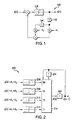
- FIG. 1 illustrates a circuit 100 having two feedback loops
- Circuit 100 is a 2-tap decision feedback equalizer (DEE).
- DEE 2-tap decision feedback equalizer
- Circuit 100 has two delay devices 102, 104 and a threshold device 106.
- delay devices 102, 104 are flip-flops.
- other devices such as registers are used,
- the output of these devices change in accordance with a clock signal.
- the performance or rate at which circuit 100 can process data is limited by a clock period of operation.
- the clock period of operation is limited by one multiply, two adds, and a thresholding (or compare) operation.
- a(n) is "0" or "1”
- multiplication by "0" or "1” is typically not a factor.
- the rate at which data is processed in a digital communications system can be increased through the use of parallelism or unfolding.
- fast DFE implementations typically reformulate the DFE loop computation based on parallel branch delayed decision techniques where all possible outputs are computed and the correct output is selected by a multiplexer.
- the multiplexer is typically controlled by one or more previous outputs, In such implementations, the feedback loop is limited to a multiplexer delay only.
- a typical propagation delay of a 2-to-1 multiplexer built using 0.13 micron photolithography technology is about 0.2 nanoseconds (ns).
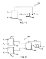
- FIG. 2 illustrates a circuit 200 formed by reformulating circuit 100 using a parallel branch delayed decision technique.
- Circuit 200 can process data at a higher rate than circuit 100.
- circuit 200 has two delay devices 202, 204, four threshold devices 206, 208, 210, 212, and a 4-to-1 multiplexer 214.
- the inputs to the four threshold devices 206, 208, 210, 212 must be computed.
- the performance of circuit 200 is inherently limited by the operating performance of multiplexer 214.
- an X-tap DFE can be reformulated and implemented using 2 x comparators and a 2 x -to-1 multiplexer.
- the speed is limited by the 2 x -to-1 multiplexer.
- the signal a(n) has "Y” possible values or levels, it can be represented using a word-length of "b" bits, where "b” equals
- PAM-Y modulated signals e.g., PAM-4 or PAM-5 modulated signals
- PAM-tap DFE can be reformulated and implemented using Y x comparators and a Y x -to-b multiplexer.
- FIG. 3 illustrates a circuit 300 that implements a serdes (serializer/descrializer) for a backplane application, which makes use of a 4-parallel embodiment of a DFE.
- circuit 300 has a DFE 302, a precursor filter 304, four analog-to-digital converters (ADC) 306a, 306b, 306c, 306d, fourpmgrammable gain amplifiers (PGA) 308a, 308b, 308c, 308d, a timing recovery circuit 310, and an automatic gain control circuit 312.
- ADC analog-to-digital converters
- PGA fourpmgrammable gain amplifiers
- a 6-tap DFE can be implemented using 64 comparators and a 64-to-1 multiplexer loop in a serial implementation.
- a 64-to-1 multiplexer loop 400 is illustrated in FIG. 4.
- 64-to-1 multiplexer loop 400 is implemented using sixty-three 2-to-1 multiplexers 402.
- 64-to-1 multiplexer loop 400 requires 32 instances of 2-to-1 multiplexer 402a, 16 instances of 2-to-1 multiplexer 402b, 8 instances of 2-to-1 multiplexer 402c, 4 instances of 2-to-1 multiplexer 402d, 2 instances of 2-to-1 multiplexer 402e, and 1 instance of 2-to-1 multiplexer 402f.
- 2-to-1 multiplexer 402f is highly loaded. Fan-out and a large capacitance typically reduce the expected performance of 64-to-1 multiplexer loop 400.
- a typical computation time for multiplexer 402f, loaded as shown in FIG. 4, is about 0.45 ns (i.e., more than twice the 0.2 ns that can be achieved if multiplexer 402f were not heavily loaded).
- 64-to-1 multiplexer loop 400 has six delay devices 404a, 404b, 404c, 404d, 404e, 404f, These six delay devices form part of six nested feedback loops. As described herein, nested feedback loops limit the applicability of known design techniques used by engineers to build high-speed digital communications systems.
- loop means a directed path that begins and ends at the same node of a circuit.
- loop bound means a calculated time, wherein the loop bound of the j-th loop of a circuit is given by EQ. 1: T j W j where T j is the loop computation time and W j is the number of delays in the loop. This point is further illustrated by the circuit in FIG. 5.
- FIG. 5 illustrates a circuit 500 having a single loop (i.e., a feedback loop).
- This single loop contains two delays (shown in FIG. 5 as a single delay device 502 such as, for example, a 2-bit shift register or 2 flip-flops in series).
- Circuit 500 has an adder 504 and a multiplier 506.
- critical loop means the loop of a circuit having the longest loop bound.
- a circuit may have more than just one critical loop.
- iteration bound means the loop bound of the critical loop of a circuit. This point is further illustrated by FIG. 6.
- FIG. 6 illustrates a circuit 600 having three loops 602, 604, 606.
- Loop 602 starts at node A, goes to node B, and returns to node A.
- Loop 602 contains a single delay 603.
- Loop 604 starts at node A, goes to node B, goes to node C, and returns to node A.
- Loop 604 contains two delays 605.
- Loop 606 starts at node B, goes to node C, goes to node D, and returns to node B.
- Loop 606 also contains two delays 607.
- the computation times of node A is 10 ns.
- the computation time of node B is 2 ns.
- the computation time of node C is 3 ns.
- the computation time of node B is 5 ns.
- the iteration bound of circuit 600 is 12 ns (i.e., the maximum of 12 ns, 7.5 ns, and 5 ns).
- every feedback loop of 64-to-1 multiplexer loop 400 is a critical loop.
- the iteration bound of 64-to-1 multiplexer loop 400 is the computation time of a single 2-to-1 multiplexer 402.
- the example starts by assuming that a maximum clocking rate of 500 MHz can be achieved, using an available manufacturing technology. Given a maximum achievable clocking rate of 500 MHz, the clocking period of the example circuit will be 2 ns. It will be assumed for purposes of the example that an iteration bound of less than 1.7 ns must be achieved in order to provide sufficient operating margin or the circuit design will be unacceptable.
- FIG. 7 illustrates a 4-unfolded multiplexer loop circuit 700, which is obtained from the 64-to-1 multiplexer loop circuit 400 shown in FIG. 4.
- Circuit 700 contains several 2-to-1 multiplexers 402 and several delays 404.
- the critical path of circuit 700 is illustrated by a dashed line 702.
- the critical path involves nine 2-to-1 multiplexers 402.
- circuit 700 does not satisfy the design criterion of having an iteration bound of less than 1.7 ns.
- retiming may be used to reduce the number of 2-to-1 multiplexers 402 in the critical path.
- FIG. 8 illustrates two cut-sets 802, 804 that can be used to reduce the number of 2-to-1 multiplexers 402 in the critical path of circuit 700.
- FIG. 9 illustrates the retimed 4-unfolded loop of FIG. 8.
- the critical path shown by a dashed line 902 now involves just four 2-to-1 multiplexers 402. This is misleading, however, because as described above, the four multiplexers (F 0 , F 1 , F 2 , and F 3 ) in the critical path are heavily loaded.
- the known techniques of unfolding and retiming cannot be applied to the nested loops of 64-to-1 multiplexer loop 400. Applying these known techniques has led to an unacceptable circuit design.
- FIGs. 10 and 11 Another known technique that can be used to improve the iteration bound of a circuit is pipelining combined with look-ahead. This technique is illustrated by FIGs. 10 and 11.
- FIG. 10 illustrates a 2-to-1 multiplexer loop circuit 1000.
- FIG. 11 illustrates a circuit 1100 that can be formed by applying pipelining and look-ahead to circuit 1000.
- Circuit 1100 has a delay 1102. a multiplexer 1104, and a multiplexer 1106 in addition to the multiplexer 1002 of circuit 1000.
- the output of circuit 1100 is given by EQ. 5, which is obtained by substituting previous iterations of EQ. 3 and EQ. 4 in EQ. 3.
- a n A n a n -1 + B n a n -1
- the known method for applying pipelining and look-ahead to circuit 1000 has improved the iteration bound by a factor of 2.
- the present invention fills this void
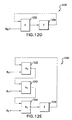
- FIG. 12A illustrates a 4-to-1 multiplexer loop circuit 1200.
- Circuit 1200 can also be thought of as forming the first two stages of any multiplexer loop that is 4-to-1 or larger.
- the first stage consists of multiplexer 1202a.
- the second stage consists of multiplexers 1202b, 1202c.
- circuit 1200 has three multiplexers 1202a, 1202b, 1202c, and two delay devices 1204a,1204b. Assuming multiplexer 1202a has a computation time of 0.4 ns (i.e., it is highly loaded) and the other two multiplexers 1202b, 1202c, each have a computation time of 0.2 ns, the iteration bound of circuit 1200 is 0.4 ns.
- circuits such as, forexample, multiplexer loop circuit 1200 can be unfolded. Unfolding circuit 1200 permits parallel processing of circuit inputs.
- FIG. 12B illustrates an example 2-unfolded circuit 1210 obtained by unfolding the multiplexer loop circuit 1200 by a factor of two.
- Circuit 1210 has two parallel processing pipelines 1212 and 1214.
- unfolding circuit 1200 increases the loading of multiplexer 1202a.
- unfolding circuit 1200 has increased the iteration bound (i.e., the iteration bound of circuit 1210 is greater than the iteration bound of circuit 1200) since the output of multiplexer 1216 is dependent upon the output of multiplexer 1202a.
- FIG. 12C illustrates an example 3-unfolded circuit 1220 obtained by unfolding the multiplexer loop circuit 1200 by a factor of three.
- Circuit 1220 has three parallel processing pipelines 1222, 1224, and 1226.
- FIG. 12D illustrates an example digital processing circuit 1230.
- Circuit 1230 includes a processing element 1232 and a delay 1234.
- Processing element 1232 can be any known processing element or network.
- Delay 1234 is part of a feedback loop that includes processing element 1232.
- FIG. 12E illustrates an example 3-unfoldeddigital processing circuit 1240 obtained by unfolding circuit 1230 by a factor of three using a conventional unfolding technique.
- This conventional unfolding technique involves adding two additional processing elements 1242 and 1244 to the feedback loop that includes processing element 1232 and delay 1234. As can be seen by a comparison of circuit 1240 to circuit 1230, this conventional unfolding technique has increased the loading of processing element 1232. This conventional unfolding technique has also produced a circuit having an increased iteration period.
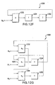
- FIG. 12F illustrates an example digital processing circuit 1250 that includes a feedback loop having two delays.
- Circuit 1250 is obtained by adding an additional delay 1252 to the feedback loop of circuit 1230 in accordance with a technique of the invention. As described herein, adding additional delays to a feedback loop in conjunction with circuit unfolding can reduce or eliminate the fan-out and iteration bound issues associated with conventional unfolding techniques.
- FIG. 12G illustrates an example 3-unfolded digital processing circuit 1260 obtained by unfolding circuit 1250 by a factor of three in accordance with a first unfolding technique of the invention.
- This unfolding technique involves adding two additional processing elements 1262 and 1264 to the feedback loop that includes processing element 1232 and delays 1234 and 1252.
- this unfolding technique of the invention has reduced the loading of processing element 1232, and it has resulted is a better iteration period.
- FIG. 12H illustrates an example 4-unfolded digital processing circuit 170 obtained by unfolding circuit 1250 by a factor of four in accordance with a second unfolding technique of the invention.
- This unfolding technique results in to independent processing networks.
- One processing network comprises processing elements 1232 and 1264.
- the other processing network comprises processing elements 1262 and 1272.
- this unfolding technique of the invention has reduced the loading of processing element 1232, and it has resulted is a better iteration bound.
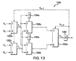
- FIG. 13 illustrates a circuit 1300 developed by applying one form of pipelining and look-ahead to circuit 1200. As described herein, this conventional form does not improve the performance of circuit 1200. It is shown only so that it can be contrasted with the present invention.
- circuit 1300 is formed by adding three delays 1302, 1304a, 1304b, and two multiplexers 1306a, 1306b to circuit 1200.
- the output of circuit 1300 is given by EQs. 7a and 7b.
- EQ. 7a is obtained by substituting past iterations of EQ. 6c in itself.
- each multiplexer 1306a,1306b Assuming the computation time of each multiplexer 1306a,1306b is 0.2 ns, the loop bound of the inner nested loop is 0.2 ns. But, the loop bound of the outer loop is 0.4 ns. Thus, as stated above, this application is not useful for improving the performance of a multiplexer loop.
- FIG. 14 illustrates a circuit 1400 developed by applying a second form of pipelining and look-ahead to circuit 1200. This form also is not very useful for improving the performance of circuit 1200. This form is also shown so that it can be contrasted with the present invention.
- the output of circuit 1400 is given by EQs. 8a and 8b.
- EQ. 8a is obtained by substituting past iterations of EQ. 6a and EQ. 6c in EQ. 6a.
- the loop bound of the inner nested loop is 0.2 ns.
- the loop bound of the outer loop is 0.3 ns. While this is an improvement over the form illustrated by FIG. 13, it still does not resolve the decreased performance of the multiplexer loop.
- applying this form of pipelining and look-ahead results in an expected iteration bound of about 1.2 ns, which is less than the 1.7 ns criterion. But, for reasons described herein, this iteration bound may not be achievable.
- the iteration bound can be reduced even further than this by applying the pipelining and look-ahead techniques of the invention. In comparison, the invention significantly increases the clock speed or symbol speed that can be achieved.
- the pipelining and look-ahead of FIG. 15A solves the issue of degraded multiplexer loop performance described above. This is because the loop bound of every feedback loop of the multiplexer loop is improved rather than just improving the performance of one loop to the detriment of another loop.
- FIG. 15A illustrates a circuit 1500, according to an embodiment of the invention, that is formed by adding a delay 1502 and four 2-to-1 multiplexers 1504a, 1504b, 1504c, 1504d to to circuit 1200.
- each of the 2-to-1 multiplexers has two input ports, one control port, and one output port.
- none of the 2-to-1 multiplexers 1504a, 1504b, 1504c, 1504d is included in a feedback loop.
- These multiplexers form part of a 1-level look-ahead network 1506.
- the extra delay added to circuit 1200 forms a part of the innermost nested loop.
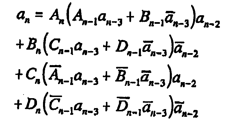
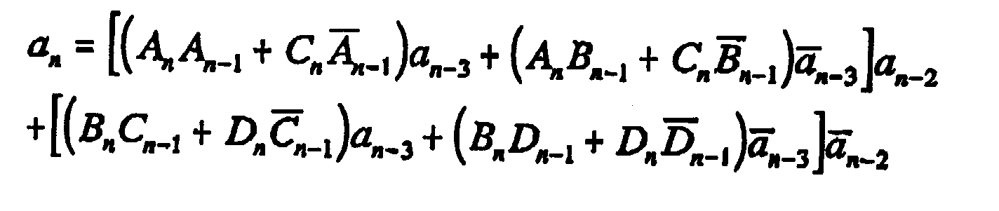
- circuit 1500 The output of circuit 1500 is given by the following equations:
- the iteration bound of circuit 1500 is 0.2 ns.
- the pipelining and look-ahead of the invention increases the performance of the nested loop without degrading the performance of the outer loop.
- the invention can be used to restore the performance of the multiplexer loop to an expected level of performance (e.g., 0.2 ns).
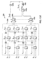
- FIG. 15B illustrates an example 2-unfolded circuit 1510 obtained by unfolding the circuit of FIG. 15A by a factor of two in accordance with the invention.
- Circuit 1510 comprises a look-ahead circuit 1512 and two parallel processing pipelines 1514 and 1516 in accordance with the invention.
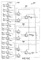
- FIG. 15C illustrates an example 3-unfolded circuit 1520 obtained by unfolding the circuit of FIG. 15A by a factor of three in accordance with the invention.
- Circuit 1520 comprises a look-ahead circuit 1522 and three parallel processing pipelines 1524, 1526, and 1528 in accordance with the invention.
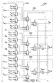
- FIG. 15D illustrates an example 4-unfolded circuit 1530 obtained by unfolding the circuit of FIG. 15A by a factor of four in accordance with the invention.
- Circuit 1530 comprises a look-ahead circuit 1532 and four parallel processing pipelines 1534, 1536, 1538, and 1540 in accordance with the invention.
- FIG. 15E illustrates a circuit 1550 having a 3-level look-ahead network 1556 according to an embodiment of the invention.
- Circuit 1550 is formed by adding a delay 1552 and 3-level look-ahead network 1556 to circuit 1200.
- each of the 2-to-1 multiplexers has two input ports, one control port, and one output port.
- the extra delay added to circuit 1200 forms a part of the innermost nested loop.
- 3-level look-ahead network 1556 is formed using multiplexers and delays. 3-level look-ahead network 1556 transforms the four input values A n , B n , C n , and D, into four intermediate values O 1 , O 2 , O 3 , and O 4 , As will be understood by persons skilled in the relevant arts, other circuits can be used to implement a 3-level look-ahead network.
- the invention can be implemented in a manner that will achieve an objective not obtainable by circuits 1300 and 1400.
- the invention can be implemented in a multiplexer loop such that the performance degradation caused by the heavy loading of multiplexer 1202a is completely eliminated without increasing the loop bound of any loop. This is achieved by adding delay to the innermost nested feedback loop and by not adding any multiplexers within a loop of the muldploxer loop.
- a benefit of adding delay to the innermost feedback loop is that it improves the loop bound of every loop forming a part of the multiplexer loop.
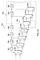
- FIG. 16 illustrates a 64-to-1 multiplexer loop circuit 1600 that incorporates the embodiment of invention shown in FIG. 15A.
- circuit 1600 is formed from multiplexer loop 400 and circuit 1500.
- the iteration bound of circuit 1600 is 0.25 ns.
- look-ahead network 1506 If look-ahead network 1506 is moved to a position between multiplexers 402c and 402d, the iteration bound of circuit is not changed (i.e, it remains at 0.25 ns). The number of multiplexers included in look-ahead network 1506, however, must be increased from 4 to 8.
- look-ahead network 1506 moving look-ahead network 1506 to a position between multiplexers 402b and 402c or to a position between multiplexers 402a and 402b also will not change the iteration bound of circuit 1600.
- the number of multiplexers included in look-ahead network 1506, however, will have be increased from 4 to 16, or 4 to 32, respectfully.
- look-ahead network 1506 If look-ahead network 1506 is moved to a location before multiplexer 402a, the iteration bound of circuit 1600 is reduced, It is reduced to 0.2 ns, and every loop of circuit 1600 becomes a critical loop.
- This design requires increasing the number of multiplexers of look-ahead network 1506 from 4 to 64. Thus, as can be seen from FIG. 16, it is advantageous to position look-ahead network 1506 in front of multiplexer 402a.
- FIG. 17 illustrates a 4-unfolded circuit 1700 having a critical path 1702.
- Critical path 1702 is illustrated by a dashed line.
- circuit 1700 is formed using circuit 1600.
- Circuit 1700 contains several 2-to-1 multiplexers 402 and several delays 404.
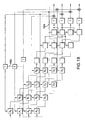
- FIG. 18 illustrates two cut-sets 1802,1804 that can be used to reduce the number of 2-to-1 multiplexers in the critical path of the circuit of FIG. 17. This will reduce the computation time of the circuit.
- FIG. 19 illustrates the retimed circuit of FIG. 16.
- This retimed circuit has two critical paths 1902, 1904,
- a clock period of operation of 1.2 ns can be achieved (i.e., 1.0 ns + 0.2 ns).
- the invention is not limited to a particular amount of look-ahead or a particular number of inputs-to-outputs, such as the 4-to-1 ratio illustrated in FIG. 15A.
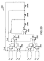
- FIG. 20 illustrates an 8-to-1 multiplexer loop 2000.
- Multiplexer loop 2000 is formed from a plurality of 2-to-1 multiplexers 2002 and a plurality of delays 2004, as shown in FIG. 20.
- FIG. 21 illustrates a circuit 2100 formed by applying the look-ahead and pipelining of the invention to circuit 2000. As shown in FIG. 21, delay 2004a has been replaced by a delay 2102, and a look-ahead network 2104 has been added. The benefits of circuit 2100 over circuit 2000 are the same as those already described herein for other circuits according to the invention.
- circuit 2100 The output of circuit 2100 is described by the following equations:
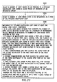
- FIG. 22 illustrates a flowchart of the steps of a method 2200 for pipelining multiplexer loops according to an embodiment invention. As described herein, pipelined multiplexer loops according to the invention can be used to form part of an integrated circuit.
- Method 2200 has three steps 2202, 2204, 2206. Each of these steps will now be described and illustrated with an example application.
- step 2202 a number of input values is selected.
- the selected number of inputs is provided to a pipelined multiplexer loop according to the invention during a clock period of operation of an integrated circuit.
- the number of selected inputs can be used to identify a particular multiplexer loop that is to be modified in accordance with the invention.
- step 2204 a number of look-ahead steps is selected.
- the number of look-ahead steps is independent of the number of input values selected in step 2202.
- the selected level of look-ahead is implemented as a part of the pipelined multiplexer loop according to the invention.
- a pipelined multiplexer loop according to the invention is implemented using, for example, a backplane or an optical/fiber technology.
- the pipelined multiplexer loop is implemented using at least one digital logic circuit according to the invention.
- the pipelined multiplexer is also implemented so that it has the number of look-ahead steps selected in step 2204.
- the digital logic circuit has an n -level look-ahead network that converts the number of input values selected in step 2202 to a plurality of intermediate values, wherein n represents the number of look-ahead steps selected in step 2204.
- the digital logic circuit is formed from a plurality of multiplexers each having a first and a second input port, an output port, and a control port. At least some of these multiplexers are arranged to form the pipelined multiplexer loop.
- the pipelined multiplexer loop has at least a first and a second stage.
- the first stage consists of a first multiplexer.
- the second stage consists of a second and a third multiplexer.
- a first communications link couples the output port of the second multiplexer to the first input port of the first multiplexer.
- a second communications link couples the output port of the third multiplexer to the second input port of the first multiplexer.
- a first feedback loop having a first delay time, couples the output port of the first multiplexer to the control port of the first multiplexer.
- a second feedback loop having a second delay time, couples the output port of the first multiplexer to the control ports of the second and third multiplexers.
- the first delay time is an integer multiple of the second delay time and is equal to (n+1) times a clock period of operation of the integrated circuit.
- method 2200 can be used to design or improve the performance of a wide variety of circuits.
- FIGs. 23-28 illustrate how method 2200 is applied to design and/or improve the performance of a DFE.
- FIG. 23 illustrates a serial representation of an example of a circuit that can be used as part of a digital communications system to remove inter-symbol interference (i.e., a DFE).
- the DFE is formed using an 8-to-1 multiplexer loop 2302 (similar to the 8-to-1 multiplexer loop 2000 described above) and several comparators 2308.
- the multiplexers 2304 of the multiplexer loop are similar to those described above, each having an expected computation time of 0.2 ns.
- the multiplexer loop has three delays 2306a, 2306b, 2306c.
- the DFE circuit of FIG. 23 can be determined after selecting, in step 2202 of method 2200, the number of input values that need to be provided to a pipelined multiplexer loop during a clock period of operation of an integrated circuit. As shown in FIG. 23, eight values are input to multiplexer loop 2302. These input values are the outputs of the eight comparators 2308. The comparators 2308 compare an input signal y n to eight possible feedback signals f 0 ... f 7 .
- the present invention can be applied to multiplexer loop 2302.
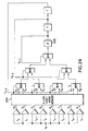
- FIG. 24 illustrates an embodiment of the 3-tap DFE of FIG. 23 having pipelining and 2-levels of look-ahead in accordance with the invention.
- the circuit of FIG. 24 can be formed from the circuit of FIG. 23 by replacing delay 2306a with a delay 2402, and by adding 2-level look-ahead network 2404.
- the delay 2402 forms a part of every loop of the multiplexer loop.
- no additional multiplexers were added to the loops of the multiplexer loop.
- 2-level look-ahead network 2404 has been placed before each of the multiplexers that form part of the multiplexer loop shown in FIG. 23.
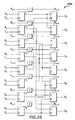
- FIG. 25 illustrates a detailed view of 2-level look-ahead network 2404.
- 2-level look-ahead network 2404 is formed using multiplexers and delays.
- 2-level look-ahead network 2404 transforms eight input values A n , B n , C n , D n , E n , F n , G n , and H n , into eight intermediate values O 1 , O 2 , O 3 , O 4 , O 5 , O 6 , O 7 , and O 8 .
- other circuits can be used to implement a 2-level look-ahead network.
- circuit according to the invention can be used to form part of a larger integrated circuit.
- circuits according to the invention are combined with comparator circuits to form an integrated circuit.
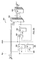
- FIG, 26 illustrates a 4-unfolded comparator circuit 2600 with f 1 -latch and pipeline-registers.
- Circuit 2600 is formed using comparators 2602, data flip-flops (DFF) 2604, and latches (LAT) 2608.
- Circuit 2600 can be used, for example, with a 4-unfolded and retimed circuit formed from the circuit of FIG. 24.
- the circuit of FIG. 24 can be unfolded and retimed in a manner similar to that described above for the circuit of FIG. 16.
- FIG. 27 illustrates a 6-bit compare circuit 2700.
- Circuit 2700 can be modified, when required, to form an n-bit compare circuit.
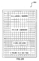
- FIG. 28 illustrates a serializer/deserializer that makes use of a 4-tap decision feedback equalizer integrated circuit 2800 according to an embodiment of the invention.
- Circuit 2800 is implemented using circuits similar to those described herein.
- Integrated circuit 2800 is illustrative and not intended to limit the invention.
- FIGs. 29A-B illustrate a flowchart of the steps of method 2900 according to an embodiment of the invention.
- Method 2900 is used to design high speed parallel processing circuits such as the ones described herein.
- high speed parallel processing circuits in accordance with the invention are designed in accordance with method 2900 as follows.
- a number of bits (B) of a bit-stream to be processed in parallel by a digital circuit is selected.
- a clocking rate (C) is selected for the digital circuit, wherein a product (P), P being equal to B times C, is equal to at least 1 gigabit per second.
- An initial circuit capable of serially processing the bits of the bit-stream at a data processing rate less than P is formed.
- This initial circuit includes a feedback loop having N+1 delays. N is a whole number greater than zero, The initial circuit is unfolded by a factor of B to form B parallel processing pipelines for the bits of the bit-stream.
- An N-step look-ahead network is formed to provide inputs to the B parallel processing pipelines.
- the N-step look-ahead network is formed by forming an initial look-ahead network in conjunction with the initial circuit and unfolding the initial look-ahead network as described herein by a factor B.
- the unfolded circuit is retimed to achieve the selected clocking rate (C).
- method 2900 involves six steps. These steps will now be described in more detail.
- step 2902 a number of bits (B) of a bit-stream to be processed in parallel by a digital circuit is selected.
- the number of bits selected for parallel processing determines the level of parallelism of the circuit.
- a clocking rate (C) is selected for the digital circuit, wherein a product (P), P being equal to B times C, is equal to at least 1 gigabit per second.
- the clock rate (C) is selected in conjunction with the value of B, selected in step 2902, so that B times C equals a desired system rate.
- the clock rate (C) equals 625 MHz (i.e., P/B equals 625,000 cycles/sec).
- a clock period (T) for the circuit equals 1.6 nanoseconds (ns).
- an initial circuit capable of serially or sequentially processing the bits of the bit-stream at a data processing rate less than P is formed.
- This initial circuit includes a feedback loop having N+1 delays, wherein N is a whole number greater than zero.
- the initial circuit is formed to have an innermost nested feedback loop, wherein the innermost nested feedback loop has N+1 delays.
- the initial circuit is formed using a multiplexer loop such as one of the multiplexer loops described above.
- the invention is not limited, however, to using a multiplexer loop to form the initial circuit.
- the initial circuit formed in step 2906 is not a final or complete circuit in accordance with the invention. Thus, the initial circuit formed in step 2906 is not intended to be built or manufactured.
- the initial circuit is unfolded by a factor of B to form B parallel processing pipelines for the bits of the bit-stream.
- the initial circuit is unfolded by a factor equal to the number of delays in the feedback loop.
- the initial circuit is unfolded by a factor less than the number of delays in the feedback loop.
- the initial circuit is unfolded by a factor greater than the number of delays in the feedback loop.
- the initial circuit can be unfolded to form at least two parallel processing circuits that are interconnected by a feedback loop. In some embodiments, however, the initial circuit is unfolded to form at least two parallel processing circuits that are not interconnected by a feedback loop. (See, e.g., FIGs. 12G and12H).
- an N-step look-ahead network is formed to provide inputs to the B parallel processing pipelines.
- look-ahead networks similar to those described and shown herein are used.
- the N-step look-ahead network is formed by forming an initial look-ahead network in conjunction with the initial circuit and unfolding the initial look-ahead network as described herein by a factor B.
- the N-step look-ahead network is formed apart from the initial circuit.
- step 2912 the unfolded circuit is retimed to achieve the selected clocking rate (C). How to retime an unfolded circuit is described above.
- the selected clocking rate (C) or clock period (T) can not be achieved by retiming the unfolded circuit, one can increase the number of delays in the feedback loop of the initial circuit, in an iterative manner, so that the corresponding unfolded and retimed circuit will achieve the selected clocking rate (C) or clock period (T).
- the unfolded and retimed circuit of step 2912 in combination with the N-step look-ahead network of step 2910 comprise a digital circuit according to an embodiment invention.
- circuits having additional unfolding such as, for example, 16-unfolded circuits can also be implemented in accordance with the invention.
- the example embodiments described herein are not intended to limit the invention. Using the invention and various degrees of unfolding, it is possible to build circuits according to the invention that operate, for example, at data rates in excess of 3 Gb/s, 5 Gb/s, and 10 Gb/s.
- the invention can be used in a wide variety of digital circuits to improve performance.
- the invention is used to improve the performance of computer processing systems having one or more nested feedback loops or multiplexer loops.
- Computer processing systems typically include microprocessors or microcontrollers having one or more instruction decoders, arithmetic logic units and/or other specialized circuits that contain multiplexers in a feedback loop. These feedback loops limit operating speed or processing speed.
- the invention can be used to improve the operating speed or processing speed of such circuits, and thereby improve system performance.
- Other types of digital circuits that can benefit from the invention will become apparent to persons skilled in the relevant arts given the description herein.
Landscapes
- Engineering & Computer Science (AREA)
- Computer Networks & Wireless Communication (AREA)
- Signal Processing (AREA)
- Power Engineering (AREA)
- Microelectronics & Electronic Packaging (AREA)
- Electronic Switches (AREA)
- Image Processing (AREA)
- Advance Control (AREA)
- Cable Transmission Systems, Equalization Of Radio And Reduction Of Echo (AREA)
Abstract
Description









Claims (42)
- A method for designing a digital circuit that operates at a data processing rate in excess of 1 gigabit per second, the method comprising:selecting a number of bits (B) of a bit-stream to be processed in parallel by a digital circuit;selecting a clocking rate (C) for the digital circuit, wherein a product (P), P being equal to B times C, is equal to at least 1 gigabit per second;forming an initial circuit capable of serially processing the bits of the bit-stream at a data processing rate less than P, the initial circuit including a feedback loop having N+1 delays, wherein N is a whole number greater than zero;unfolding the initial circuit by a factor of B to form B parallel processing pipelines for the bits of the bit-stream;forming an N-step look-ahead network to provide inputs to the B parallel processing pipelines; andretiming the unfolded circuit to achieve the selected clocking rate (C).
- The method of claim 1, wherein said unfolding step comprises:unfolding the initial circuit by a factor equal to the number of delays in the feedback loop.
- The method of claim 1, wherein said unfolding step comprises:unfolding the initial circuit by a factor less than the number of delays in the feedback loop.
- The method of claim 1, wherein said unfolding step comprises:unfolding the initial circuit by a factor greater than the number of delays in the feedback loop.
- The method of claim 1, wherein said step of forming the initial circuit comprises:wherein the innermost nested feedback loop has N+1 delays.forming the initial circuit to have an innermost nested feedback loop,
- The method of claim 5, wherein said unfolding step comprises:unfolding the initial circuit by a factor equal to the number of delays in the innermost nested feedback loop.
- The method of claim 5, wherein said unfolding step comprises:unfolding the initial circuit by a factor less than the number of delays in the innermost nested feedback loop.
- The method of claim 5, wherein said unfolding step comprises:unfolding the initial circuit by a factor greater than the number of delays in the innermost nested feedback loop.
- The method of claim 1, wherein said step of forming the initial circuit comprises:forming the initial circuit using a multiplexer loop.
- The method of claim 1, wherein said unfolding step comprises:unfolding the initial circuit to form at least two parallel processing circuits that are interconnected by a feedback loop.
- The method of claim 1, wherein said unfolding step comprises:unfolding the initial circuit to form at least two parallel processing circuits that are not interconnected by a feedback loop.
- The method of claim 1, wherein said step of forming the N-step look-ahead network comprises:forming an initial look-ahead network; andunfolding the initial look-ahead network by the factor B.
- A digital circuit designed by the method of claim 1.
- A decision feedback equalizer, comprising the digital circuit of claim 13.
- A transceiver, comprising the digital circuit of claim 13.
- A digital circuit that operates at a data processing rate in excess of 1 gigabit per second, comprising:an N-level look-ahead network that converts a plurality of input values from a bit-Stream to a plurality of intermediate values; andat least two parallel processing pipelines electrically coupled to the N-level look-ahead network, the at least two parallel processing pipelines being formed by:unfolding an initial circuit capable of serially processing the bits of the bit-stream, the initial circuit including a feedback loop having N+1 delays, wherein N is a whole number greater than zero, andretiming the unfolded circuit to achieve a selected clocking rate.
- The digital circuit of claim 16, wherein the initial circuit is unfolded by a factor less than the number of delays in the feedback loop.
- The digital circuit of claim 16, wherein the initial circuit is unfolded by a factor equal to the number of delays in the feedback loop.
- The digital circuit of claim 16, wherein the initial circuit is unfolded by a factor greater than the number of delays in the feedback loop.
- The digital circuit of claim 16, wherein the digital circuit forms part of a decision feedback equalizer.
- The digital circuit of claim 16, wherein the digital circuit forms part of a transceiver.
- The method of claim 16, wherein the N-level look-ahead network is formed by forming an initial look-ahead network and unfolding the initial look-ahead network.
- A digital logic circuit for determining an output value based on a plurality of inputs values, comprising:wherein the first delay time is an integer multiple of the second delay time and is equal to (n+1) times a clock period of operation of the digital logic circuit.an n-level look-ahead network that converts the plurality of input values to a plurality of intermediate values;a plurality of multiplexers each having a first and a second input port, an output port, and a control port, the plurality of multiplexers arranged to form a pipelined multiplexer loop having at least a first and a second stage, the first stage consisting of a first multiplexer, and the second stage consisting of a second and a third multiplexer, the pipelined multiplexer loop being coupled to the n-level look-ahead network;a first communications link that couples the output port of the second multiplexer to the first input port of the first multiplexer;a second communications link that couples the output port of the third multiplexer to the second input port of the first multiplexer;a first feedback loop that couples the output port of the first multiplexer to the control port of the first multiplexer, the first feedback loop comprising a first delay device having a first delay time; anda second feedback loop that couples the output port of the first multiplexer to the control ports of the second and third multiplcxers, the second feedback loop comprising the first delay device and a second delay device having a second delay time,
- The digital logic circuit of claim 23, wherein the n-level look-ahead network is a 2-level look-ahead network.
- The digital logic circuit of claim 23, wherein each of the plurality of multiplexers is a 2-to-1 multiplexer.
- The digital logic circuit of claim 23, wherein the digital logic circuit forms part of a computer processing system.
- The digital logic circuit of claim 23, wherein the digital logic circuit forms part of a transceiver.
- The digital logic circuit of claim 23, wherein the first delay time is nominally two times longer than the second delay time.
- The digital logic circuit of claim 23, wherein the first delay device and the second delay device each comprise at least one data flip-flop.
- The digital logic circuit of claim 23, wherein the digital logic circuit forms part of a communications system operating at a data rate of at least 3 gigabits per second.
- The digital logic circuit of claim 23, wherein the digital logic circuit forms part of a decision feedback equalizer.
- A digital logic circuit for determining an output value based on a plurality of inputs values, comprising:wherein the first delay time is an integer multiple of the second delay time and is equal to (n+1) times a clock period of operation of the digital logic circuit.an n-level look-ahead network that converts the plurality of input values to a plurality of intermediate values;a plurality of multiplexers each having a first and a second input port, an output port, and a control port, the plurality of multiplexers arranged to form a pipelined multiplexer loop, the pipelined multiplexer loop being coupled to the n-level look-ahead network;a first communications link that couples the output port of a first multiplexer to the first input port of a second multiplexer;a second communications link that couples the output port of a third multiplexer to the second input port of the second multiplexer;a first feedback loop that couples the output port of the second multiplexer to the control port of the second multiplexer, the first feedback loop comprising a first delay device having a first delay time; anda second feedback loop that couples the output port of the second multiplexer to the control ports of the first and third multiplexers, the second feedback loop comprising the first delay device and a second delay device having a second delay time,
- The digital logic circuit of claim 32, wherein the digital logic circuit forms part of a transceiver.
- The digital logic circuit of claim 32, wherein the digital logic circuit forms part of a computer processing system.
- The digital logic circuit of claim 32, wherein the first delay device and the second delay device each comprise at least one data flip-flop.
- The digital logic circuit of claim 32, wherein the digital logic circuit forms part of a communications system operating at a data rate of at least 3 gigabits per second.
- The digital logic circuit of claim 32, wherein the digital logic circuit forms part of a decision feedback equalizer.
- A method for pipelining multiplexer loops that form part of an integrated circuit, the method comprising the steps of:wherein the first delay time is an integer multiple of the second delay time and is equal to (n+1) times a clock period of operation of the integrated circuit.(a) selecting a number of input values to be provided to a pipelined multiplexer loop during a clock period of operation of the integrated circuit;(b) selecting a number of look-ahead steps to be implemented as a part of the pipelined multiplexer loop; and(c) implementing the pipelined multiplexer loop using at least one digital logic circuit, comprising;an n-level look-ahead network that converts the number of input values selected in step (1) to a plurality of intermediate values, wherein n represents the number of look-ahead steps selected in step (2),a plurality of multiplexers each having a first and a second input port, an output port, and a control port, the plurality of multiplexers arranged to form the pipelined multiplexer loop, the pipelined multiplexer loop having at least a first and a second stage, the first stage consisting of a first multiplexer, and the second stage consisting of a second and a third multiplexer, the pipelined multiplexer loop being coupled to the n-level look-ahead network,a first communications link that couples the output port of the second multiplexer to the first input port of the first multiplexer,a second communications link that couples the output port of the third multiplexer to the second input port of the first multiplexer,a first feedback loop, having a first delay time, that couples the output port of the first multiplexer to the control port of the first multiplexer, anda second feedback loop, having a second delay time, that couples the output port of the first multiplexer to the control ports of the second and third multiplexers,
- The method of claim 38, wherein step (3) further comprising the step of:implementing the pipelined multiplexer loop of the at least one digital logic circuit in a communications system.
- The method of claim 38, wherein step (3) further comprising the step of:implementing the pipelined multiplexer loop of the at least one digital logic circuit in a computer processing system.
- The method of claim 38, further comprising the step of:operating the pipelined multiplexer loop of the at least one digital logic circuit at a rate sufficient to process data at a rate equal to at least 3 gigabits per second.
- The method of claim 38, further comprising the step of:redistributing the first time delay and the second time delay using retiming techniques.
Applications Claiming Priority (4)
| Application Number | Priority Date | Filing Date | Title |
|---|---|---|---|
| US55910 | 2002-01-28 | ||
| US10/055,910 US7239652B2 (en) | 2002-01-28 | 2002-01-28 | Pipelining of multiplexer loops in a digital circuit |
| US147049 | 2002-05-17 | ||
| US10/147,049 US7333580B2 (en) | 2002-01-28 | 2002-05-17 | Pipelined parallel processing of feedback loops in a digital circuit |
Publications (2)
| Publication Number | Publication Date |
|---|---|
| EP1355462A2 true EP1355462A2 (en) | 2003-10-22 |
| EP1355462A3 EP1355462A3 (en) | 2006-10-04 |
Family
ID=28677765
Family Applications (1)
| Application Number | Title | Priority Date | Filing Date |
|---|---|---|---|
| EP03001717A Withdrawn EP1355462A3 (en) | 2002-01-28 | 2003-01-27 | Pipelined parallel processing of feedback loops in a decision feedback equaliser |
Country Status (2)
| Country | Link |
|---|---|
| US (1) | US7333580B2 (en) |
| EP (1) | EP1355462A3 (en) |
Families Citing this family (35)
| Publication number | Priority date | Publication date | Assignee | Title |
|---|---|---|---|---|
| US7239652B2 (en) * | 2002-01-28 | 2007-07-03 | Broadcom Corporation | Pipelining of multiplexer loops in a digital circuit |
| US7697641B2 (en) * | 2004-06-28 | 2010-04-13 | L-3 Communications | Parallel DSP demodulation for wideband software-defined radios |
| US7656339B2 (en) * | 2008-06-06 | 2010-02-02 | Lsi Corporation | Systems and methods for analog to digital conversion |
| WO2009148458A1 (en) * | 2008-06-06 | 2009-12-10 | Lsi Corporation | Systems and methods for latch based analog to digital conversion |
| US8121186B2 (en) * | 2008-06-06 | 2012-02-21 | Lsi Corporation | Systems and methods for speculative signal equalization |
| EP2198519A4 (en) * | 2008-06-06 | 2012-10-31 | Lsi Corp | Systems and methods for synchronous, retimed analog to digital conversion |
| US7656340B2 (en) * | 2008-06-06 | 2010-02-02 | Lsi Corporation | Systems and methods for pipelined analog to digital conversion |
| US20100138575A1 (en) | 2008-12-01 | 2010-06-03 | Micron Technology, Inc. | Devices, systems, and methods to synchronize simultaneous dma parallel processing of a single data stream by multiple devices |
| US20100174887A1 (en) | 2009-01-07 | 2010-07-08 | Micron Technology Inc. | Buses for Pattern-Recognition Processors |
| US8442106B2 (en) * | 2009-12-14 | 2013-05-14 | Lsi Corporation | Floating-tap decision feedback equalizer for communication channels with severe reflection |
| US9323994B2 (en) | 2009-12-15 | 2016-04-26 | Micron Technology, Inc. | Multi-level hierarchical routing matrices for pattern-recognition processors |
| US8574960B2 (en) * | 2010-02-03 | 2013-11-05 | Stats Chippac, Ltd. | Semiconductor device and method of forming cavity adjacent to sensitive region of semiconductor die using wafer-level underfill material |
| US8193961B2 (en) | 2010-09-23 | 2012-06-05 | Lsi Corporation | Systems and methods for enhancing analog to digital conversion resolution |
| US9443156B2 (en) * | 2011-12-15 | 2016-09-13 | Micron Technology, Inc. | Methods and systems for data analysis in a state machine |
| US20130275709A1 (en) | 2012-04-12 | 2013-10-17 | Micron Technology, Inc. | Methods for reading data from a storage buffer including delaying activation of a column select |
| US9524248B2 (en) | 2012-07-18 | 2016-12-20 | Micron Technology, Inc. | Memory management for a hierarchical memory system |
| US9071479B2 (en) | 2012-08-24 | 2015-06-30 | Credo Semiconductor (Hong Kong) Limited | High-speed parallel decision feedback equalizer |
| US9703574B2 (en) | 2013-03-15 | 2017-07-11 | Micron Technology, Inc. | Overflow detection and correction in state machine engines |
| US9448965B2 (en) | 2013-03-15 | 2016-09-20 | Micron Technology, Inc. | Receiving data streams in parallel and providing a first portion of data to a first state machine engine and a second portion to a second state machine |
| WO2016109570A1 (en) | 2014-12-30 | 2016-07-07 | Micron Technology, Inc | Systems and devices for accessing a state machine |
| WO2016109571A1 (en) | 2014-12-30 | 2016-07-07 | Micron Technology, Inc | Devices for time division multiplexing of state machine engine signals |
| US11366675B2 (en) | 2014-12-30 | 2022-06-21 | Micron Technology, Inc. | Systems and devices for accessing a state machine |
| US9699007B2 (en) | 2015-08-31 | 2017-07-04 | Huawei Technologies Co., Ltd. | Pipeline multiplexer loop architecture for decision feedback equalizer circuits |
| US9692618B2 (en) | 2015-09-30 | 2017-06-27 | Huawei Technologies Co., Ltd. | Pipeline multiplexer loop architecture for decision feedback equalizer circuits |
| US10691964B2 (en) | 2015-10-06 | 2020-06-23 | Micron Technology, Inc. | Methods and systems for event reporting |
| US10977309B2 (en) | 2015-10-06 | 2021-04-13 | Micron Technology, Inc. | Methods and systems for creating networks |
| US10846103B2 (en) | 2015-10-06 | 2020-11-24 | Micron Technology, Inc. | Methods and systems for representing processing resources |
| US10146555B2 (en) | 2016-07-21 | 2018-12-04 | Micron Technology, Inc. | Adaptive routing to avoid non-repairable memory and logic defects on automata processor |
| US10268602B2 (en) | 2016-09-29 | 2019-04-23 | Micron Technology, Inc. | System and method for individual addressing |
| US10019311B2 (en) | 2016-09-29 | 2018-07-10 | Micron Technology, Inc. | Validation of a symbol response memory |
| US9935800B1 (en) | 2016-10-04 | 2018-04-03 | Credo Technology Group Limited | Reduced complexity precomputation for decision feedback equalizer |
| US10929764B2 (en) | 2016-10-20 | 2021-02-23 | Micron Technology, Inc. | Boolean satisfiability |
| US10592450B2 (en) | 2016-10-20 | 2020-03-17 | Micron Technology, Inc. | Custom compute cores in integrated circuit devices |
| US12197510B2 (en) | 2016-10-20 | 2025-01-14 | Micron Technology, Inc. | Traversal of S portion of a graph problem to be solved using automata processor |
| US10728059B1 (en) | 2019-07-01 | 2020-07-28 | Credo Technology Group Limited | Parallel mixed-signal equalization for high-speed serial link |
Family Cites Families (9)
| Publication number | Priority date | Publication date | Assignee | Title |
|---|---|---|---|---|
| US5642382A (en) * | 1995-03-01 | 1997-06-24 | Hitachi America, Ltd. | Fir filters with multiplexed inputs suitable for use in reconfigurable adaptive equalizers |
| US5757855A (en) * | 1995-11-29 | 1998-05-26 | David Sarnoff Research Center, Inc. | Data detection for partial response channels |
| US6266366B1 (en) | 1998-04-30 | 2001-07-24 | Mysticom Ltd. | Digital base-band receiver with pipeline processor |
| US6363112B1 (en) | 1998-12-07 | 2002-03-26 | Agere Systems Guardian Corp. | Parallel processing decision feedback equalizer |
| US6192072B1 (en) | 1999-06-04 | 2001-02-20 | Lucent Technologies Inc. | Parallel processing decision-feedback equalizer (DFE) with look-ahead processing |
| US7933341B2 (en) | 2000-02-28 | 2011-04-26 | Broadcom Corporation | System and method for high speed communications using digital signal processing |
| US20020181575A1 (en) | 2001-05-29 | 2002-12-05 | Koninklijke Philips Electronics N.V. | Circuitry for Mitigating performance loss associated with feedback loop delay in decision feedback equalizer and method therefor |
| US7190754B1 (en) * | 2001-12-24 | 2007-03-13 | Rambus Inc. | Transceiver with selectable data rate |
| US7239652B2 (en) | 2002-01-28 | 2007-07-03 | Broadcom Corporation | Pipelining of multiplexer loops in a digital circuit |
-
2002
- 2002-05-17 US US10/147,049 patent/US7333580B2/en not_active Expired - Fee Related
-
2003
- 2003-01-27 EP EP03001717A patent/EP1355462A3/en not_active Withdrawn
Also Published As
| Publication number | Publication date |
|---|---|
| EP1355462A3 (en) | 2006-10-04 |
| US20030142698A1 (en) | 2003-07-31 |
| US7333580B2 (en) | 2008-02-19 |
Similar Documents
| Publication | Publication Date | Title |
|---|---|---|
| US7333580B2 (en) | Pipelined parallel processing of feedback loops in a digital circuit | |
| US8861583B2 (en) | Apparatus and methods for equalizer adaptation | |
| EP2590374B1 (en) | Flexible receiver architecture | |
| US9112740B2 (en) | Decision feedback equalizer | |
| KR102240293B1 (en) | System and method for maintaining high speed communication | |
| US7239652B2 (en) | Pipelining of multiplexer loops in a digital circuit | |
| CN108781195B (en) | Method and apparatus for providing high speed equalization | |
| US6192072B1 (en) | Parallel processing decision-feedback equalizer (DFE) with look-ahead processing | |
| US20090225900A1 (en) | Data transmitting circuit and transmitting method | |
| Parhi | Design of multigigabit multiplexer-loop-based decision feedback equalizers | |
| KR20060120160A (en) | Transparent Multimode PAM Interface | |
| Meybodi et al. | Design and implementation of an on-demand maximum-likelihood sequence estimation (MLSE) | |
| US12057974B2 (en) | Decision feed forward equalization for partial response equalized signal including pre-cursor cancelation | |
| US8699558B1 (en) | Decoupling and pipelining of multiplexer loop in parallel processing decision-feedback circuits | |
| US6577689B1 (en) | Timing recovery system for a 10 BASE-T/100 BASE-T ethernet physical layer line interface | |
| US11831475B1 (en) | Receiver using pseudo partial response maximum likelihood sequence detection | |
| Kim et al. | A loop-break decision feedback equalizer for DAC/ADC-DSP-based wireline transceivers | |
| CN114337602B (en) | Digital filtering using combined approximate summation of partial products | |
| EP0537407A1 (en) | Flexible encoding method and architecture for high-speed data transmission and storage | |
| US9166832B1 (en) | Methods and apparatus for decision feedback equalization adaptation | |
| CN112751552B (en) | Adaptive receiver with front cursor elimination | |
| Lin et al. | High-performance VLSI architecture of decision feedback equalizer for gigabit systems | |
| WO2017219533A1 (en) | Multiplexer loop architecture for decision feedback equalizer circuits | |
| Lin et al. | Concurrent digital adaptive decision feedback equalizer for 10GBase-LX4 ethernet system | |
| Yu et al. | Multirate digital squarer architectures |
Legal Events
| Date | Code | Title | Description |
|---|---|---|---|
| PUAI | Public reference made under article 153(3) epc to a published international application that has entered the european phase |
Free format text: ORIGINAL CODE: 0009012 |
|
| AK | Designated contracting states |
Kind code of ref document: A2 Designated state(s): AT BE BG CH CY CZ DE DK EE ES FI FR GB GR HU IE IT LI LU MC NL PT SE SI SK TR |
|
| AX | Request for extension of the european patent |
Extension state: AL LT LV MK RO |
|
| PUAL | Search report despatched |
Free format text: ORIGINAL CODE: 0009013 |
|
| AK | Designated contracting states |
Kind code of ref document: A3 Designated state(s): AT BE BG CH CY CZ DE DK EE ES FI FR GB GR HU IE IT LI LU MC NL PT SE SI SK TR |
|
| AX | Request for extension of the european patent |
Extension state: AL LT LV MK RO |
|
| 17P | Request for examination filed |
Effective date: 20070404 |
|
| RAP1 | Party data changed (applicant data changed or rights of an application transferred) |
Owner name: BROADCOM CORPORATION |
|
| AKX | Designation fees paid |
Designated state(s): DE FR GB |
|
| 17Q | First examination report despatched |
Effective date: 20081028 |
|
| STAA | Information on the status of an ep patent application or granted ep patent |
Free format text: STATUS: THE APPLICATION IS DEEMED TO BE WITHDRAWN |
|
| 18D | Application deemed to be withdrawn |
Effective date: 20120801 |