EP1355411A1 - Power apparatus - Google Patents
Power apparatus Download PDFInfo
- Publication number
- EP1355411A1 EP1355411A1 EP02710341A EP02710341A EP1355411A1 EP 1355411 A1 EP1355411 A1 EP 1355411A1 EP 02710341 A EP02710341 A EP 02710341A EP 02710341 A EP02710341 A EP 02710341A EP 1355411 A1 EP1355411 A1 EP 1355411A1
- Authority
- EP
- European Patent Office
- Prior art keywords
- directional switch
- alternating current
- specified time
- zero
- power apparatus
- Prior art date
- Legal status (The legal status is an assumption and is not a legal conclusion. Google has not performed a legal analysis and makes no representation as to the accuracy of the status listed.)
- Granted
Links
Images



Classifications
-
- H—ELECTRICITY
- H02—GENERATION; CONVERSION OR DISTRIBUTION OF ELECTRIC POWER
- H02M—APPARATUS FOR CONVERSION BETWEEN AC AND AC, BETWEEN AC AND DC, OR BETWEEN DC AND DC, AND FOR USE WITH MAINS OR SIMILAR POWER SUPPLY SYSTEMS; CONVERSION OF DC OR AC INPUT POWER INTO SURGE OUTPUT POWER; CONTROL OR REGULATION THEREOF
- H02M1/00—Details of apparatus for conversion
- H02M1/42—Circuits or arrangements for compensating for or adjusting power factor in converters or inverters
- H02M1/4208—Arrangements for improving power factor of AC input
-
- H—ELECTRICITY
- H02—GENERATION; CONVERSION OR DISTRIBUTION OF ELECTRIC POWER
- H02M—APPARATUS FOR CONVERSION BETWEEN AC AND AC, BETWEEN AC AND DC, OR BETWEEN DC AND DC, AND FOR USE WITH MAINS OR SIMILAR POWER SUPPLY SYSTEMS; CONVERSION OF DC OR AC INPUT POWER INTO SURGE OUTPUT POWER; CONTROL OR REGULATION THEREOF
- H02M1/00—Details of apparatus for conversion
- H02M1/14—Arrangements for reducing ripples from DC input or output
-
- H—ELECTRICITY
- H02—GENERATION; CONVERSION OR DISTRIBUTION OF ELECTRIC POWER
- H02M—APPARATUS FOR CONVERSION BETWEEN AC AND AC, BETWEEN AC AND DC, OR BETWEEN DC AND DC, AND FOR USE WITH MAINS OR SIMILAR POWER SUPPLY SYSTEMS; CONVERSION OF DC OR AC INPUT POWER INTO SURGE OUTPUT POWER; CONTROL OR REGULATION THEREOF
- H02M1/00—Details of apparatus for conversion
- H02M1/12—Arrangements for reducing harmonics from AC input or output
-
- Y—GENERAL TAGGING OF NEW TECHNOLOGICAL DEVELOPMENTS; GENERAL TAGGING OF CROSS-SECTIONAL TECHNOLOGIES SPANNING OVER SEVERAL SECTIONS OF THE IPC; TECHNICAL SUBJECTS COVERED BY FORMER USPC CROSS-REFERENCE ART COLLECTIONS [XRACs] AND DIGESTS
- Y02—TECHNOLOGIES OR APPLICATIONS FOR MITIGATION OR ADAPTATION AGAINST CLIMATE CHANGE
- Y02B—CLIMATE CHANGE MITIGATION TECHNOLOGIES RELATED TO BUILDINGS, e.g. HOUSING, HOUSE APPLIANCES OR RELATED END-USER APPLICATIONS
- Y02B70/00—Technologies for an efficient end-user side electric power management and consumption
- Y02B70/10—Technologies improving the efficiency by using switched-mode power supplies [SMPS], i.e. efficient power electronics conversion e.g. power factor correction or reduction of losses in power supplies or efficient standby modes
Definitions
- the present invention relates to a power apparatus to supply electric power to equipment, systems and the like by the use of a rectifying system formed of a bridge rectifier circuit.
- FIG. 7 shows a typical full-wave rectification circuit utilizing a bridge rectifier circuit.
- the full-wave rectification circuit of FIG. 7 has a bridge rectifier circuit formed of four of diodes 2 to 5.
- Reference numeral 11 indicates a load.
- FIG. 7(a) is a diagram to show an electric current flow from alternating current power source 1 during negative half a cycle of the alternating current.
- the electric currents flow through diode 4, smoothing capacitor 7 and diode 3 in this order, thereby allowing positive voltage Vo to be tapped off. More specifically, an alternating input from alternating current power source 1 is subjected to full-wave rectification and a positive direct current voltage is obtained.
- a prior art power apparatus as described in above presents such problems as a low power factor and an increased content of power supply harmonics since input currents flow only during the period when the voltage of alternating current power source 1 is higher than the direct current output voltage.
- the present invention deals with the foregoing problems and aims at providing a power apparatus whereby both a high power factor and suppression of harmonics are allowed to be achieved.
- a power apparatus of the present invention comprises:
- turning on the bi-directional switch at a suitable phase and for a suitable conducting duration allows both the suppression of harmonics in input currents and the enhanced power factor to be realized and also allows a higher direct current output voltage than the peak voltage of the alternating current power source to be obtained.
- the power apparatus of the present invention is provided with a power source frequency detecting means to set specified time ⁇ d from zero-crossing to a different fixed value based on power source frequencies, thereby allowing the control of the bi-directional switch to be facilitated.
- the bi-directional switch drive signal generating means generates an on-signal at specified time ⁇ d (0 ⁇ ⁇ d) from a zero-crossing of the input voltage and generates an off-signal at specified time ⁇ t (0 ⁇ ⁇ t) after the on-time, thereby enabling the controlling of both the harmonics in input currents from the alternating current power source and the output voltage appearing across both ends of the smoothing capacitor.
- variable range of specified time ⁇ t after the on time is limited to less than conducting duration ⁇ to of the bi-directional switch for generating a direct current output voltage needed at the time of a maximum load, thereby allowing the output voltage to be prevented from increasing to a higher value than necessary at the time of low loading.
- the power apparatus of the present invention has a load detecting means and also has a storing means inside of the bi-directional switch drive signal generating means to store in advance a combination of specified time ⁇ d from the zero-crossing and specified time ⁇ t after the on-time, both being determined according to the magnitude of load, and further selectively retrieves from the storing means based on the output of the load detecting means a combination of specified time ⁇ d from the zero-crossing and specified time ⁇ t after the on-time according to the magnitude of load, thereby allowing the power apparatus to be operated constantly at the optimum point of performance against a variety of changes in loading condition.
- FIG. 1 shows block diagrams, each illustrating the structure of a power apparatus in an exemplary embodiment of the present invention.
- Each respective power apparatus of FIG. 1(a), FIG. 1(b), FIG. 1(c) and FIG. 1(d) is provided with bridge rectifier circuit 6 formed of four diodes of diodes 2 to 5 and alternating current power source 1.
- bridge rectifier circuit 6 formed of four diodes of diodes 2 to 5 and alternating current power source 1.
- reactor 8 connected between alternating current power source 1 and the alternating current input end of bridge rectifier circuit 6 and capacitor 10 connected between the alternating current input end and the direct current output end of bridge rectifier circuit 6.
- capacitor 10 is connected between alternating current end 6a or 6b and negative direct current output end 6c of bridge rectifier circuit 6 via bi-directional switch 9, and in the block diagrams of FIG. 1(c) and FIG. 1(d), capacitor 10 is connected between alternating current end 6a or 6b and positive direct current output end 6d of bridge rectifier circuit 6.
- smoothing capacitor 7 is connected between positive direct current output end 6d and negative direct current output end 6c of bridge rectifier circuit 6, thereby making it possible for the violently changing direct currents from bridge rectifier circuit 6 to be smoothed out as a direct current.
- each respective power apparatus of the foregoing has zero-crossing detecting means 12 to detect zero-crossing of the voltage of alternating current power source 1, bi-directional switch drive signal generating means 13 to generate a drive signal for bi-directional switch based on an output of zero-crossing detecting means 12 and bi-directional switch driving means 14 to drive bi-directional switch 9 based on an output of bi-directional switch drive signal generating means 13.
- the entries of zero-crossing detecting means 12, bi-directional switch drive signal generating means 13 and bi-directional switch driving means 14 are omitted.
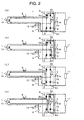
- FIG. 2(a) and FIG. 2(b) illustrate what takes place in the power apparatus during the positive half period of alternating input voltage Vi
- FIG. 2(c) and FIG. 2(d) illustrate what takes place during the negative half period of the same
- FIG. 3(a) and FIG. 3(b) show the performance of the power apparatus of FIG. 1(a) in terms of waveforms at various points and the like of the unit under the conditions that Vi is 200 V, L is 10 mH, C is 300 ⁇ F and Co is 1800 ⁇ F.
- FIG. 3(a) shows the respective waveforms of alternating input voltage Vi, currents IL(alternating input current) flowing in reactor 8, direct current output voltage Vo and bi-directional switch driving signal voltage Vg and FIG. 3(b) shows the respective waveforms of alternating input voltage Vi, currents Ic flowing in capacitor 10 and voltage Vc across both ends of capacitor 10.
- bi-directional switch 9 is turned off immediately after the zero-crossing of alternating input voltage Vi in a positive alternating half period, direct current output voltage Vo is higher than alternating.
- input voltage Vi and diodes 2 and 5 are reverse-biased, thereby allowing no input currents to be flowing.
- bi-directional switch drive signal generating means 13 In specified time ⁇ d after alternating input voltage Vi crosses the zero point from the negative period domain to the positive period domain, bi-directional switch drive signal generating means 13 generates an on-signal for bi-directional switch 9 and electric currents start flowing in the direction indicated by an arrow in FIG. 2(a) upon turning on bi-directional switch 9 through bi-directional switch driving means 14.
- electric currents flow from alternating current power source 1 through reactor 8, diode 2, smoothing capacitor 7 and capacitor 10 in succession, thereby causing capacitor 10 to discharge and ending up with a resulting reduction of capacitor voltage Vc to Vc1 or less.
- the specified time ⁇ d from the zero-crossing point is selected so as to have the summation of alternating input voltage Vi and capacitor voltage Vc1 of capacitor 10 made larger than direct current voltage Vo of smoothing capacitor 7, thereby making bi-directional switch 9 turn on.
- bi-directional switch drive signal generating means 13 generates an off-signal for bi-directional switch 9 and, upon turning off bi-directional switch 9 through bi-directional switch driving means 14, electric currents flow from alternating current power source 1 through reactor 8, diode 2, smoothing capacitor 7 and diode 5 in succession while capacitor 10 maintaining capacitor voltage Vc2 at the time of turning bi-directional switch 9 off, thereby causing capacitor voltage Vc to be reduced to zero finally due to the decline of alternating input voltage Vi.
- Bi-directional switch 9 is turned off immediately after the zero-crossing of alternating input voltage Vi in a negative alternating half period, direct current output voltage Vo is higher than alternating input voltage Vi and diodes 3 and 4 are reverse-biased, thereby allowing no input currents to be flowing.
- bi-directional switch drive signal generating means 13 In specified time ⁇ d after alternating input voltage Vi crosses the zero point from the positive period domain to the negative period domain, bi-directional switch drive signal generating means 13 generates an on-signal for bi-directional switch 9 and electric currents start flowing in the direction indicated by an arrow in FIG. 2(c) upon turning on bi-directional switch 9 through bi-directional switch driving means 14.
- bi-directional switch drive signal generating means 13 generates an off-signal for bi-directional switch 9 and, upon turning off bi-directional switch 9 through bi-directional switch driving means 14, capacitor 10 maintains capacitor voltage Vc1 by being charged up to that voltage level of Vc1 and electric currents flow from alternating current power source 1 through diode 4, smoothing capacitor 7, diode 3 and reactor 8 in succession, as FIG. 2(d) shows, and finally capacitor voltage Vc is reduced to zero due to the decline of alternating input voltage Vi.
- the input currents are allowed to flow at a point of time closer to the zero-crossing point of the input voltage than with a prior art power apparatus, thereby achieving the enhancement of power factor.
- the electric currents flowing in the power apparatus are series resonance currents flowing through reactor 8 and capacitor 10 or smoothing capacitor 7, the electric currents increase less abruptly in comparison with the case where a reactor is used to form a short circuit as seen generally in a step-up circuit, thereby making it possible for the whine of reactor 8 to be suppressed.
- the series resonance currents due to reactor 8 and capacitor 10 or smoothing capacitor 7 have no high frequency ringing components and therefore, by making an appropriate selection of inductance L of reactor 8, capacitance C of capacitor 10, specified time ⁇ d from the zero-crossing point and specified time ⁇ t after the turning-on time, harmonics can be effectively prevented from being generated.
- 3(c) shows an example of the comparisons between the harmonic components of the input current and the Japanese domestic-guide line 15 relative to the regulation on harmonics. It is found out from FIG. 3(c) that the harmonic components of the input current are less than the limits of the guide line in magnitude.
- the horizontal axis shows the order of harmonics and the vertical axis shows the magnitude of electric currents.
- a power apparatus in exemplary embodiment 2 of the present invention is characterized by limiting the variable range of specified time ⁇ t after the turning-on time not to exceed conducting duration ⁇ to of the bi-directional switch, during which a direct current output voltage needed for the maximum load is generated.
- the power apparatus of the present invention is characterized by storing energy in reactor 8 and capacitor 10 in the conducting duration of bi-directional switch 9 during half a negative cycle of alternating current input voltage Vi and releasing the foregoing stored energy to smoothing capacitor 7 during half a positive cycle of alternating current input voltage Vi.
- the power apparatus of the present invention has the so-called step-up action.
- output voltage Vo increases as specified time ⁇ t after the turning-on time increases and the value of output voltage Vo is dependent on the magnitude of load, thereby making output voltage Vo after the same turning-on time the higher as the magnitude of load becomes the smaller. Therefore, there is a possibility of making output voltage Vo extraordinarily high when specified time ⁇ t after the turning-on time is made excessively large under light load, thereby bringing output voltage Vo to a level that exceeds the withstand voltage of smoothing capacitor 7.
- the maximum value of specified time ⁇ t after the turning-on time is limited to less than conducting duration ⁇ to, during which output voltage Vo needed for the maximum load is generated, as described before. Accordingly, the conducting duration of bi-directional switch 9 is limited to less than ⁇ to even under light load, thereby allowing the output voltage to be prevented from increasing extraordinarily.
- FIG. 5 is a schematic diagram of a power apparatus that has such additions to the power apparatus in exemplary embodiment 1 (FIG. 1) as load detecting means 16 and storing means 13a located inside bi-directional switch drive signal generating means 13 to store specified time ⁇ d from the zero-crossing point and specified time ⁇ t after the turning-on time.
- FIG. 6 is a schematic diagram of a power apparatus that has such an addition to the power apparatus in exemplary embodiment 3 (FIG. 5) as power source frequency detecting means 12a. Based on the output of power source frequency detecting means 12a, specified time ⁇ d from the zero-crossing point is set up via bi-directional switch drive signal generating means 13.
- the power source frequency is detected by power source frequency detecting means 12a and then transmitted to bi-directional switch drive signal generating means 13, thereby allowing bi-directional switch drive signal generating means 13 to set up specified time ⁇ d from the zero-crossing point determined in advance according to the power source frequency.
- bi-directional switch driving means 14 drives bi-directional switch 9.
- specified time ⁇ d from the zero-crossing point is set up and controlled according to the variation in power source frequency, specified time ⁇ d from the zero-crossing point is kept as a certain value in the ordinary load variation region, thereby allowing the controlling steps to be simplified and also allowing an appropriate power factor, output voltage value and harmonics suppression effect to be realized regardless of the variation in power source frequency.
- Zero-crossing detecting means 12 bi-directional switch drive signal generating means 13, bi-directional switch driving means 14, load detecting means 16, power source frequency detecting means 12a, storing means 13a and the like as described in above are allowed to be realized by the use of circuit arrangements formulated mainly around microcomputers and the like and also program software. (Such circuit arrangements are not shown in the drawings.)
- a capacitor is connected via a bi-directional switch between an alternating current input end and a direct current output end of a bridge rectifier circuit, thereby driving a bi-directional switch appropriately.
- the present invention achieves such an advantage as allowing a power apparatus, which can satisfy both requirements of an enhanced power factor and harmonics suppression and also can control a direct current output voltage, to be made available.
Landscapes
- Engineering & Computer Science (AREA)
- Power Engineering (AREA)
- Rectifiers (AREA)
- Ac-Ac Conversion (AREA)
Abstract
Description
Claims (7)
- A power apparatus comprising an alternating current power source, a bridge rectifier circuit to subject alternating currents from said alternating current power source to full-wave rectification and a smoothing capacitor connected to a direct current output end of said bridge rectifier circuit, further comprising:(a) a reactor connected between said alternating current power source and an alternating current input end of said bridge rectifier circuit;(b) a capacitor connected via a bi-directional switch between said alternating current input end and direct current output end of said bridge rectifier circuit;(c) a zero-crossing detecting means to detect a zero voltage point of said alternating current power source;(d) a bi-directional switch drive signal generating means to generate a drive signal for said bi-directional switch based on an output of said zero-crossing detecting means; and(e) a bi-directional switch driving means to drive said bi-directional switch based on a signal of said bi-directional switch drive signal generating means.
- The power apparatus according to claim 1, wherein said bi-directional switch drive signal generating means generates an on-signal in specified time Δd from zero-crossing.
- The power apparatus according to claim 2, further comprising a power source frequency detecting means to set specified time Δd from zero-crossing to a different fixed value based on power frequencies.
- The power apparatus according to claim 2, wherein said bi-directional switch drive signal generating means' generates an off-signal in specified time Δt after an on-signal is generated.
- The power apparatus according to claim 4, wherein specified time Δt starting from an on-time and ending at a time, when an off-signal is generated, is determined based on a direct current output voltage corresponding to a load demand.
- The power apparatus according to claim 4, wherein a variable range of specified time Δt from an on-time is restricted not to exceed conducting duration Δ to of a bi-directional switch for generating a direct current output voltage needed at a time of maximum load.
- The power apparatus according to claim 2 or claim 5, further comprising a load detecting means and also a storing means inside a bi-directional switch drive signal generating means to store in advance a combination of specified time Δd from zero-crossing and specified time Δt after an on-time, both being determined according to a magnitude of load, wherein a combination of specified time Δd from zero-crossing and specified time Δt after an on-time, both being determined according to a magnitude of load, is retrieved selectively from said storing means to bring the power apparatus into operation.
Applications Claiming Priority (3)
| Application Number | Priority Date | Filing Date | Title |
|---|---|---|---|
| JP2001018202A JP3729072B2 (en) | 2001-01-26 | 2001-01-26 | Power supply |
| JP2001018202 | 2001-01-26 | ||
| PCT/JP2002/000497 WO2002060044A1 (en) | 2001-01-26 | 2002-01-24 | Power apparatus |
Publications (3)
| Publication Number | Publication Date |
|---|---|
| EP1355411A1 true EP1355411A1 (en) | 2003-10-22 |
| EP1355411A4 EP1355411A4 (en) | 2006-12-20 |
| EP1355411B1 EP1355411B1 (en) | 2015-11-11 |
Family
ID=18884260
Family Applications (1)
| Application Number | Title | Priority Date | Filing Date |
|---|---|---|---|
| EP02710341.5A Expired - Lifetime EP1355411B1 (en) | 2001-01-26 | 2002-01-24 | Rectifier with high power factor and low harmonics |
Country Status (6)
| Country | Link |
|---|---|
| US (1) | US6671192B2 (en) |
| EP (1) | EP1355411B1 (en) |
| JP (1) | JP3729072B2 (en) |
| KR (1) | KR100822515B1 (en) |
| CN (2) | CN2560157Y (en) |
| WO (1) | WO2002060044A1 (en) |
Families Citing this family (20)
| Publication number | Priority date | Publication date | Assignee | Title |
|---|---|---|---|---|
| JP2006109622A (en) * | 2004-10-06 | 2006-04-20 | Matsushita Electric Ind Co Ltd | Electric equipment |
| TW200636420A (en) * | 2004-12-14 | 2006-10-16 | Int Rectifier Corp | An EMI noise reduction circuit and method for bridgeless PFC circuit |
| JP2006288134A (en) * | 2005-04-04 | 2006-10-19 | Matsushita Electric Ind Co Ltd | Power supply |
| JP5044939B2 (en) * | 2006-01-30 | 2012-10-10 | パナソニック株式会社 | DC power supply |
| KR100823922B1 (en) * | 2006-03-14 | 2008-04-22 | 엘지전자 주식회사 | DC power supply and its method |
| KR100883502B1 (en) * | 2008-09-02 | 2009-02-16 | 이성고 | Automatic harmonic control device |
| CN102244460A (en) * | 2010-05-11 | 2011-11-16 | 联昌电子企业股份有限公司 | Power Conversion System for Zero-Voltage Startup and Its Zero-Voltage Startup Device |
| US8400797B2 (en) * | 2010-07-23 | 2013-03-19 | Lien Chang Electronic Enterprise Co., Ltd. | Power conversion system with zero-voltage start-up mechanism, and zero-voltage start-up device |
| KR101127373B1 (en) | 2010-08-06 | 2012-03-29 | 리엔 창 일렉트로닉 엔터프라이즈 컴퍼니 리미티드 | Power conversion system with zero-voltage start-up mechanism, and zero-voltage start-up device |
| JP5753971B2 (en) * | 2010-11-19 | 2015-07-22 | パナソニックIpマネジメント株式会社 | Power supply |
| FR2991833B1 (en) * | 2012-06-06 | 2015-12-18 | Valeo Sys Controle Moteur Sas | ABSORPTION CIRCUIT FOR POWER RIPPING ASSOCIATED METHOD |
| CN102969880B (en) * | 2012-12-14 | 2015-01-14 | 山东大学 | Second ripple removing circuit of single-phase voltage-type convertor |
| CN103944365B (en) * | 2014-04-14 | 2016-05-18 | 山东大学 | A kind of Single-phase PWM Rectifier is eliminated secondary ripple circuit |
| JP6443655B2 (en) * | 2014-06-30 | 2018-12-26 | 工機ホールディングス株式会社 | Motor drive device and electric tool |
| TWI581555B (en) * | 2014-09-12 | 2017-05-01 | Alpha And Omega Semiconductor (Cayman) Ltd | Fixed on-time switching converter |
| WO2017014143A1 (en) * | 2015-07-21 | 2017-01-26 | 三菱電機株式会社 | Electric power converting device |
| US20170104409A1 (en) * | 2015-10-12 | 2017-04-13 | Texas Instruments Incorporated | Adaptive bus voltage auto-selection system |
| KR102109144B1 (en) * | 2017-09-29 | 2020-05-28 | 주식회사 아모센스 | Apparatus and method for controlling power |
| DE102019002098A1 (en) * | 2019-03-23 | 2020-09-24 | Leopold Kostal Gmbh & Co. Kg | Voltage converter for direct current |
| WO2021166186A1 (en) * | 2020-02-20 | 2021-08-26 | 三菱電機株式会社 | Dc power supply device, refrigeration cycle device, air conditioner, and refrigerator |
Family Cites Families (11)
| Publication number | Priority date | Publication date | Assignee | Title |
|---|---|---|---|---|
| JPS58222782A (en) * | 1982-06-18 | 1983-12-24 | Hitachi Ltd | Controller for pwm converter |
| JP3225825B2 (en) * | 1996-01-12 | 2001-11-05 | 富士電機株式会社 | AC / DC converter |
| US5793624A (en) * | 1996-06-05 | 1998-08-11 | Hydro-Quebec | Apparatus and method for charging a DC battery |
| US6137700A (en) * | 1997-10-08 | 2000-10-24 | Daikin Industries, Ltd. | Converter with a high power factor using a DC center point voltage |
| JP3272299B2 (en) | 1998-04-28 | 2002-04-08 | 三洋電機株式会社 | Drive circuit |
| US6181583B1 (en) * | 1999-01-19 | 2001-01-30 | Matsushita Electric Industrial Co., Ltd. | Power supply device and air conditioner using the same |
| JP3377959B2 (en) | 1999-02-17 | 2003-02-17 | 松下電器産業株式会社 | Power supply |
| JP2000295853A (en) * | 1999-04-02 | 2000-10-20 | Daikin Ind Ltd | Multi-level converter |
| US6320772B1 (en) * | 1999-05-26 | 2001-11-20 | Matsushita Electric Industrial Co., Ltd. | Converter circuit having control means with capability to short-circuit converter output |
| JP2001028879A (en) * | 1999-07-13 | 2001-01-30 | Mitsubishi Electric Corp | Supply power control device |
| US6407936B1 (en) * | 2001-03-13 | 2002-06-18 | Astec International Limited | Capacitive boost for line harmonic improvement in power converters |
-
2001
- 2001-01-26 JP JP2001018202A patent/JP3729072B2/en not_active Expired - Fee Related
-
2002
- 2002-01-24 EP EP02710341.5A patent/EP1355411B1/en not_active Expired - Lifetime
- 2002-01-24 WO PCT/JP2002/000497 patent/WO2002060044A1/en not_active Ceased
- 2002-01-24 US US10/239,784 patent/US6671192B2/en not_active Expired - Fee Related
- 2002-01-25 KR KR1020020004355A patent/KR100822515B1/en not_active Expired - Fee Related
- 2002-01-25 CN CN02202157U patent/CN2560157Y/en not_active Expired - Fee Related
- 2002-01-25 CN CNB021028591A patent/CN1243404C/en not_active Expired - Fee Related
Also Published As
| Publication number | Publication date |
|---|---|
| EP1355411A4 (en) | 2006-12-20 |
| JP2002223571A (en) | 2002-08-09 |
| CN1243404C (en) | 2006-02-22 |
| EP1355411B1 (en) | 2015-11-11 |
| WO2002060044A1 (en) | 2002-08-01 |
| CN2560157Y (en) | 2003-07-09 |
| US20030165070A1 (en) | 2003-09-04 |
| JP3729072B2 (en) | 2005-12-21 |
| KR20020063126A (en) | 2002-08-01 |
| CN1367573A (en) | 2002-09-04 |
| WO2002060044A8 (en) | 2003-11-13 |
| US6671192B2 (en) | 2003-12-30 |
| KR100822515B1 (en) | 2008-04-16 |
Similar Documents
| Publication | Publication Date | Title |
|---|---|---|
| US6671192B2 (en) | Power apparatus | |
| US7532491B2 (en) | Apparatus and method for supplying DC power source | |
| JP3422218B2 (en) | converter | |
| US7613018B2 (en) | Apparatus and method for supplying DC power source | |
| EP0859453B1 (en) | Power supply circuit for a control circuit | |
| JPH07177745A (en) | Switching regulator | |
| US20130135911A1 (en) | Ac-dc converter | |
| EP1298782A2 (en) | Inverter air-conditioner | |
| US7719139B2 (en) | Power supply unit | |
| KR100881253B1 (en) | Power unit | |
| HU223161B1 (en) | Generator for arc welding machines | |
| JP4572595B2 (en) | CONVERTER CONTROL METHOD, CONVERTER CONTROL DEVICE, AIR CONDITIONER, ITS CONTROL METHOD AND CONTROL DEVICE | |
| EP1601089B1 (en) | Power supply apparatus and an air conditioner using the same | |
| JPH1198847A (en) | Rectifier circuit | |
| KR100292489B1 (en) | Power factor correcting boost converter using soft switching technique | |
| JP4722541B2 (en) | Power supply device and air conditioner using the same | |
| JP2005341746A (en) | DC power supply | |
| JP2006149021A (en) | DC power supply device and compressor driving device using the same | |
| WO1994013057A1 (en) | Power converter circuit | |
| JP2008099510A (en) | DC power supply and equipment using it | |
| JP2005341747A (en) | Power supply | |
| JP2008072778A (en) | DC power supply | |
| JP2006121837A (en) | Power supply | |
| JP2005269796A (en) | Power supply | |
| KR20050021133A (en) | Inverter circuit including compensable power factor |
Legal Events
| Date | Code | Title | Description |
|---|---|---|---|
| PUAI | Public reference made under article 153(3) epc to a published international application that has entered the european phase |
Free format text: ORIGINAL CODE: 0009012 |
|
| 17P | Request for examination filed |
Effective date: 20020925 |
|
| AK | Designated contracting states |
Kind code of ref document: A1 Designated state(s): AT BE CH CY DE DK ES FI FR GB GR IE IT LI LU MC NL PT SE TR |
|
| A4 | Supplementary search report drawn up and despatched |
Effective date: 20061120 |
|
| REG | Reference to a national code |
Ref country code: DE Ref legal event code: 8566 |
|
| RAP1 | Party data changed (applicant data changed or rights of an application transferred) |
Owner name: PANASONIC CORPORATION |
|
| 17Q | First examination report despatched |
Effective date: 20090309 |
|
| REG | Reference to a national code |
Ref country code: DE Ref legal event code: R079 Free format text: PREVIOUS MAIN CLASS: H02M0007120000 Ipc: H02M0001120000 |
|
| RIC1 | Information provided on ipc code assigned before grant |
Ipc: H02M 1/42 20070101ALI20150626BHEP Ipc: H02M 1/12 20060101AFI20150626BHEP |
|
| GRAP | Despatch of communication of intention to grant a patent |
Free format text: ORIGINAL CODE: EPIDOSNIGR1 |
|
| INTG | Intention to grant announced |
Effective date: 20150828 |
|
| RBV | Designated contracting states (corrected) |
Designated state(s): ES GR IT |
|
| GRAS | Grant fee paid |
Free format text: ORIGINAL CODE: EPIDOSNIGR3 |
|
| GRAA | (expected) grant |
Free format text: ORIGINAL CODE: 0009210 |
|
| AK | Designated contracting states |
Kind code of ref document: B1 Designated state(s): ES GR IT |
|
| PG25 | Lapsed in a contracting state [announced via postgrant information from national office to epo] |
Ref country code: ES Free format text: LAPSE BECAUSE OF FAILURE TO SUBMIT A TRANSLATION OF THE DESCRIPTION OR TO PAY THE FEE WITHIN THE PRESCRIBED TIME-LIMIT Effective date: 20151111 |
|
| PG25 | Lapsed in a contracting state [announced via postgrant information from national office to epo] |
Ref country code: GR Free format text: LAPSE BECAUSE OF FAILURE TO SUBMIT A TRANSLATION OF THE DESCRIPTION OR TO PAY THE FEE WITHIN THE PRESCRIBED TIME-LIMIT Effective date: 20160212 |
|
| PLBE | No opposition filed within time limit |
Free format text: ORIGINAL CODE: 0009261 |
|
| STAA | Information on the status of an ep patent application or granted ep patent |
Free format text: STATUS: NO OPPOSITION FILED WITHIN TIME LIMIT |
|
| 26N | No opposition filed |
Effective date: 20160812 |
|
| PGFP | Annual fee paid to national office [announced via postgrant information from national office to epo] |
Ref country code: IT Payment date: 20180129 Year of fee payment: 17 |
|
| PG25 | Lapsed in a contracting state [announced via postgrant information from national office to epo] |
Ref country code: IT Free format text: LAPSE BECAUSE OF NON-PAYMENT OF DUE FEES Effective date: 20190124 |