EP1355326A2 - Resistor and method for producing the resistor - Google Patents
Resistor and method for producing the resistor Download PDFInfo
- Publication number
- EP1355326A2 EP1355326A2 EP03009011A EP03009011A EP1355326A2 EP 1355326 A2 EP1355326 A2 EP 1355326A2 EP 03009011 A EP03009011 A EP 03009011A EP 03009011 A EP03009011 A EP 03009011A EP 1355326 A2 EP1355326 A2 EP 1355326A2
- Authority
- EP
- European Patent Office
- Prior art keywords
- resistor
- good solvent
- binder resin
- conductive filler
- solvent
- Prior art date
- Legal status (The legal status is an assumption and is not a legal conclusion. Google has not performed a legal analysis and makes no representation as to the accuracy of the status listed.)
- Granted
Links
Images




Classifications
-
- H—ELECTRICITY
- H01—ELECTRIC ELEMENTS
- H01C—RESISTORS
- H01C17/00—Apparatus or processes specially adapted for manufacturing resistors
- H01C17/06—Apparatus or processes specially adapted for manufacturing resistors adapted for coating resistive material on a base
- H01C17/065—Apparatus or processes specially adapted for manufacturing resistors adapted for coating resistive material on a base by thick film techniques, e.g. serigraphy
- H01C17/06506—Precursor compositions therefor, e.g. pastes, inks, glass frits or green body
- H01C17/06593—Precursor compositions therefor, e.g. pastes, inks, glass frits or green body characterised by the temporary binder
-
- H—ELECTRICITY
- H01—ELECTRIC ELEMENTS
- H01C—RESISTORS
- H01C10/00—Adjustable resistors
- H01C10/30—Adjustable resistors the contact sliding along resistive element
- H01C10/305—Adjustable resistors the contact sliding along resistive element consisting of a thick film
- H01C10/306—Polymer thick film, i.e. PTF
-
- H—ELECTRICITY
- H01—ELECTRIC ELEMENTS
- H01C—RESISTORS
- H01C17/00—Apparatus or processes specially adapted for manufacturing resistors
- H01C17/06—Apparatus or processes specially adapted for manufacturing resistors adapted for coating resistive material on a base
- H01C17/065—Apparatus or processes specially adapted for manufacturing resistors adapted for coating resistive material on a base by thick film techniques, e.g. serigraphy
- H01C17/06506—Precursor compositions therefor, e.g. pastes, inks, glass frits or green body
- H01C17/06573—Precursor compositions therefor, e.g. pastes, inks, glass frits or green body characterised by the permanent binder
- H01C17/06586—Precursor compositions therefor, e.g. pastes, inks, glass frits or green body characterised by the permanent binder composed of organic material
-
- Y—GENERAL TAGGING OF NEW TECHNOLOGICAL DEVELOPMENTS; GENERAL TAGGING OF CROSS-SECTIONAL TECHNOLOGIES SPANNING OVER SEVERAL SECTIONS OF THE IPC; TECHNICAL SUBJECTS COVERED BY FORMER USPC CROSS-REFERENCE ART COLLECTIONS [XRACs] AND DIGESTS
- Y10—TECHNICAL SUBJECTS COVERED BY FORMER USPC
- Y10T—TECHNICAL SUBJECTS COVERED BY FORMER US CLASSIFICATION
- Y10T29/00—Metal working
- Y10T29/49—Method of mechanical manufacture
- Y10T29/49002—Electrical device making
- Y10T29/49082—Resistor making
-
- Y—GENERAL TAGGING OF NEW TECHNOLOGICAL DEVELOPMENTS; GENERAL TAGGING OF CROSS-SECTIONAL TECHNOLOGIES SPANNING OVER SEVERAL SECTIONS OF THE IPC; TECHNICAL SUBJECTS COVERED BY FORMER USPC CROSS-REFERENCE ART COLLECTIONS [XRACs] AND DIGESTS
- Y10—TECHNICAL SUBJECTS COVERED BY FORMER USPC
- Y10T—TECHNICAL SUBJECTS COVERED BY FORMER US CLASSIFICATION
- Y10T29/00—Metal working
- Y10T29/49—Method of mechanical manufacture
- Y10T29/49002—Electrical device making
- Y10T29/49082—Resistor making
- Y10T29/49099—Coating resistive material on a base
Definitions
- the present invention relates to a resistor used for a variable resistor, a switch and other electronic input devices, and it particularly has an object to provide a resistor capable of minimizing the contact resistance of the surface of the resistor with a sliding contact or contact member, and a method for producing the resistor.
- a resistor used for a variable resistor, a switch contact or the like is formed as film on a substrate in a prescribed thickness.
- a mixed solution of a thermosetting binder resin, a solvent for dissolving the binder resin, and a conductive filler such as carbon black is applied onto the surface of the substrate by means of screen printing or the like.
- the solvent is vaporized in a drying process followed by baking to cure the binder resin.
- the resistance characteristic of the above-mentioned resistor is determined depending on the quantity of the filler in the binder resin which forms the resistor, and also influenced by the dispersion state of the conductive filler in the binder resin.
- the change quantity of resistance value is minimized when the sliding contact is moved by a short distance, and the range between maximum resistance value and minimum resistance value obtained from the variable resistor is also minimized, so that the high resolution cannot be ensured.
- the contact resistance is increased when the total resistance of the resistor of the variable resistor is set high as above, the ratio of the error portion by the contact resistance to the resistance value set by the movement of the sliding contact is increased to make it difficult to precisely set the correspondence of the moving position of the sliding contact to the resistance value corresponding thereto.
- the present invention has an object to provide a resistor cable of minimizing the contact resistance with a sliding contact or contact member without significantly reducing the total resistance value by making the resistance in the surface of the resistor smaller than the resistance in the inner part thereof, and a method for producing this resistor.
- the present invention involves a resistor formed of a conductive resin material comprising a binder resin and a conductive filler mixed to the binder resin, wherein when compared between a surface of the resistor and an internal cross section parallel to the surface of the resistor on the basis of regions partitioned in the same area, dispersity of the conductive filler in the binder resin is lower in the surface than in the cross section.
- the degree of dispersity of the conductive filler can be defined as follows.
- the one having a larger maximum dimension of two or more aggregates of the conductive filler is defined as the one having low dispersity. According to this definition, the maximum dimension of the aggregates of the conductive filler is larger in the surface than in the cross section of the resistor.
- the one having a larger maximum diameter of two or more virtual circles drawable in a part free from the conductive filler is defined as the one having low dispersity.
- the maximum diameter of the virtual circles is larger in the surface than in the cross section of the resistor.
- the method for producing a resistor according to the present invention comprises:
- the poor solvent is dominant in the surface of the resistor because the good solvent is vaporized first. Therefore, in the baked resistor, the dispersity of the conductive filler can be reduced in the surface to reduce the contact resistance with the sliding contact or contact member. Since the good solvent and the poor solvent are hardly vaporized in the inner part of the resistor, and present therein for a long time, the dispersity of the conductive filler is enhanced. Accordingly, in the baked resistor, the internal resistance can be increased to increase the total resistance value of the resistor.
- a boiling point of the poor solvent is preferably higher than the boiling point of the good solvent, and a difference between both the boiling points is preferably 15 °C or higher and 30 °C or lower.
- the drying process is preferably carried out at a temperature higher than the boiling point of the good solvent and lower than the boiling point of the poor solvent.
- the good solvent is, for example, at least one or more of dipropylene glycol monomethyl ether, diethylene glycol monomethyl ether, diethylene glycol monoethyl ether, and dipropylene glycol monoethyl ether
- the poor solvent is at least one or more of terpineol, 2-phenoxy ethanol, and 2-benzyloxy ethanol.
- the resistor according to the present invention has a prescribed resistance value, and an electronic input device using this resistor is constituted as a one in which a sliding contact or contact member makes contact with the resistor.
- the resistance value corresponding to the position from the end part of the resistor to the sliding contact is variably set by sliding the sliding contact on the resistor formed in a rectangular pattern or ring-like pattern.
- the resistor has a prescribed resistance value, and the set resistance value of the resistor is read when the contact member makes contact therewith.
- Fig. 8 is a perspective view showing a linear type variable resistor as one example of an electronic input device to which a resistor as an embodiment of the present invention is applied.
- the resistor 1 is formed on the surface of a substrate 2.
- the resistor 1 has a strip shape having a prescribed thickness and a fixed width dimension.
- Electrodes 3 and 4 formed of a conductive material smaller in specific resistance than the resistor 1 are conductively provided on both end parts located in the vertical (longitudinal) direction of the resistor 1.
- a sliding contact 5 is in contact with the surface of the resistor 1.
- the sliding contact 5 is formed of, for example, a phosphor bronze plate having a silver-plated surface, the specific resistance of which is smaller than the resistor 1.
- the contact part 5a of the sliding contact 5 is circularly bent, and the contact part 5a is vertically (longitudinally) slid on the surface of the resistor in the state where it is in contact with the surface of the resistor 1.
- the set values of the sliding contact 5 with the electrodes 3, 4 are changed according to the moving position of the sliding contact 5.
- Fig. 1A is a TEM (transmission electron microscopic) picture of the surface of the resistor 1
- Fig. 1B is a TEM picture of an internal cross section parallel to the surface of the resistor.
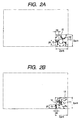
- Fig. 2A is a schematic view of the transferred dispersion state of the conductive filler in a 2 ⁇ m ⁇ 2 ⁇ m partitioned region at the right lower angle part in the TEM picture of Fig. 1A.
- Fig. 2B is similarly a schematic view of the transferred dispersion state of the conductive filler in a 2 ⁇ m ⁇ 2 ⁇ m partitioned region at the right lower angle part in the TEM picture of Fig. 1B.
- the binder resin is cured in the state where the conductive filler is contained in the binder resin.
- the binder resin is a thermosetting resin, including, for example, a polyimide resin (hereinafter referred to as resin).
- the conductive filler of the resistor shown in Fig. 1 is carbon black, and the resin is mixed with the carbon black in a mass ratio of 85:15.
- the resistor 1 shown in the TEM pictures of Figs. 1A and B has a film thickness of 10 ⁇ m.
- Fig. 1A shows the surface of the resistor, and the cross section of Fig. 1B is located 0.2 ⁇ m inward from the surface.
- the dispersion state of the carbon black 12 within the resin 11 is differed, and the carbon black 12 is dispersed more uniformly in the cross section of the resistor 1 than in the surface with the higher dispersity.
- the degree of dispersity of the carbon black 12 (conductive filler) is defined as follows.
- the one having the larger maximum dimension of two or more aggregates of carbon black is defined as the one having low dispersity.
- the maximum dimension of the aggregates is larger in the surface than in the cross section.
- Fig. 2A the largest aggregate of the carbon black 12 in the partitioned region is denoted at 13, and in Fig. 2B, the largest aggregate of the carbon black 12 in the partitioned region is denoted at 14.
- xa and ya are the width dimensions of the aggregate 13
- xb and yb are the width dimensions of the aggregate 14.
- the state where the dispersity is higher in the surface than in the partitioned region means that at least one condition of xa > xb and ya > yb is satisfied, preferably, the both are satisfied. More preferably, at least one of the magnification of xa to xb and the magnification of ya to yb is 1.5 times or more.
- the one having the larger maximum diameter of two or more virtual circles drawable in the part free from the conductive filler is defined as the one having low dispersity.
- the maximum diameter of the virtual circles is larger in the surface than in the cross section.
- the largest virtual circle is denoted at 15, and in Fig. 2B, the largest virtual circle is denoted at 16. It can be understood from Figs. 2 that the diameter of the virtual circle 15 is larger than the diameter of the virtual circle 16.
- the ratio of diameter size of the virtual circles is preferably 1.5 times or more, more preferably, 2 times or more.
- the comparison may be performed in partitioned regions having the same area in different positions if they are in the same resistor.
- the resistance value of the surface can be minimized while increasing the total resistance value or without significantly reducing the total resistance value.
- the total resistance value with the electrodes 3 and 4 can be increased even if the vertical (longitudinal) dimension of the resistor 1 is minimized.
- the change quantity of resistance value to the moving quantity in the movement of the sliding contact 5 can be also increased.
- the contact resistance between the resistor 1 and the sliding contact 5 can be minimized, the dispersion in the relation between the sliding position in the movement of the sliding contact 5 and the resistance value (output value) can be minimized, and a variable resistor with high resolution and high performance can be thus obtained.
- the resistor 1 can be produced by screen-printing a mixed solution on the substrate 2, and drying it followed by baking.
- the mixed solution is a mixture of the above-mentioned polyimide resin, a solvent for dissolving the resin, and the carbon black.
- a low-boiling point good solvent with high solubility to the resin and high volatility and a high-boiling point poor solvent lower in solubility than the good solvent and lower in volatility than the good solvent are used.
- diethylene glycol monoethyl ether H5C2OC2H4OC2H4OH; boiling point 202 °C
- terpineol boiling point 219 °C
- the good solvent and the poor solvent were mixed in a mass ratio of 1:1, the mixture of both the solvent was mixed with the resin in a mass ratio of 1:1, and the carbon black was further mixed thereto in the above-mentioned ratio.
- the mixed solution is pattern-formed on the surface of the substrate 2 such as ceramic substrate or glass epoxy substrate excellent in heat resistance and insulating property by means of screen printing or the like.
- the printed substrate is put in a drying furnace, and dried at a prescribed temperature for a prescribe time, and the solvent is vaporized by this drying to solidify the mixed solution.
- the resin that is the thermosetting resin is crosslinked and hardened in a polymer state. Consequently, the resistor 1 comprising the carbon black dispersed in the inner part can be obtained.
- the good solvent with low boiling point vaporizes first in the surface of the film-formed mixed solvent, and the poor solvent with high boiling point is dominantly present in the surface for a long time.
- This poor solvent is low in solubility to the resin (binder resin) , resulting in the large particle size of the resin dissolved in the mixed solution, and the deterioration of the dispersion state of carbon black. Accordingly, the dispersity of carbon black is deteriorated in the surface of the resistor 1 as shown in Fig. 1A after backing.
- the inner part of the film-formed mixed solution is interrupted from air, the vaporization of both the good solvent and the poor solvent is delayed, compared with in the surface, and both the solvents are present in the inner part over a long time. Accordingly, the dispersion state of the resin within the mixed solvent is improved by the action of the good solvent, and the particle size of the resin in the mixed solution is minimized to provide a satisfactory dispersion state of carbon black. Accordingly, when the mixed solution is dried by the vaporization of the poor solvent and good solvent, the carbon black is uniformly dispersed in the inner part.
- the dispersity of carbon black lowers in the surface of the resistor 1 as shown in Fig. 1A to reduce the resistance value, and the dispersity of carbon black increases in the inner part of the resistor 1 as shown in Fig. 1B to keep a high resistance value.
- Fig. 3 is a TEM picture of a mixed solution as a comparative example obtained by mixing diethylene glycol monoethyl ether (H5C2OC2H4OC2H4OH; boiling point 202 °C) that is the good solvent to the resin in a mass ratio of 1:1, and then mixing carbon black thereto
- Fig. 4 is a TEM picture of a mixed solution as another comparative example obtained by mixing terpineol that is the good solvent to the resin in a mass ratio of 1:1 and then mixing carbon black thereto.
- Figs. 3 and 4 show that the carbon black is uniformly dispersed with the resin in the mixed solution using only the good solvent as in Fig. 3, and the carbon black is present in an aggregated state clinging to the resin in the mixed solution using only the poor solvent as shown in Fig. 4.
- the mixed use of the good solvent and the poor solvent as in the above embodiment allows a structure in which the dissolving function of the poor solvent shown in Fig. 4 is dominant in the surface of the resistor 1, and the dissolving function of the good solvent shown in Fig. 3 is dominant in the inner part.
- Fig. 5 shows a further comparative example.
- a film 10 ⁇ m thick is pattern-formed by use of a mixed solution obtained by mixing the diethylene glycol monoethyl ether shown in Fig 3 to the resin in a mass ratio of 1:1, and then mixing the carbon black thereto, and it is dried followed by baking to obtain a resistor.
- Fig. 5A is a TEM picture of the surface of the resulting resistor
- Fig. 5B is a TEM picture of the cross section thereof in the same position as in Fig. 1B.
- the carbon black is uniformly dispersed in both the surface and the inner part of the resistor of this comparative example, and the resistance value is high in both the surface and inner part. Accordingly, in a variable resistor using the resistor shown in Fig. 5, the maximum resistance value can be increased, but the contact resistance with the sliding contact is also increased.
- any alcohol-based or ether-based low-boiling point solvent having a boiling point ranging from 190 °C to 210 °C is usable.
- any alcohol-based high-boiling point solvent having a cyclic alkyl or aromatic ring which has a boiling point of 215 °C or higher is usable.
- the above-mentioned terpineol, 2-phenoxy ethanol (boiling point 245 °C), and 2-benzyloxy ethanol (boiling point 256 °C) are usable alone or in combination of two or more thereof.
- the terpineol has the following chemical formula:
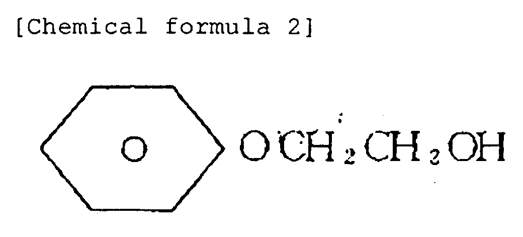
- the 2-phenoxy ethanol has the following chemical formula:
- the 2-benzyloxy ethanol has the following chemical formula:
- the combination of the good solvent and the poor solvent may be optionally selected.
- the temperature difference in boiling point between the poor solvent and the good solvent is preferably within the range of 15 to 30 °C.
- the temperature in the drying process is preferably higher than the boiling point of the good solvent and lower than the boiling point of the poor solvent.
- the conductive filler in addition to carbon black, graphite and other carbon fibers, and mixed bodies thereof can be used as the conductive filler.
- the resistor shown in Figs. 1A and B is taken as a working example, and the resistor shown in Figs. 5A and 5B which is formed by use of only the good solvent shown in Fig. 3 is taken as a comparative example.
- the linear sliding type variable resistor shown in Fig. 8 was manufactured by use of the resistor of the working example and the resistor of the comparative example.
- the thickness of the resistor was set to 10 ⁇ m
- the plane shape was set to a vertical (longitudinal) dimension of 12 mm and a width dimension of 2.7 mm.
- the temperature in the drying process was set to 170 °C, 190 °C, 200 °C, 210 °C, and 220 °C, and the drying time at the respective temperature was set to 10, 7 and 5 minutes.
- the baking temperature was set to 380 °C, and the time to 100 minutes.
- the temperature in the drying process was set to 160 °C, 170 °C, 180 °C, 190 °C, 200 °C, 210 °C, 220 °C, 230 °C, 240 °C, and 250 °C, and the drying time at the respective temperature was set to 10, 7, and 5 minutes .
- the baking temperature was set to 380 °C, and the time to 100 minutes similarly to the working example.
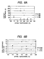
- Fig. 6A shows the contact resistance ( ⁇ ) of each resistor based on the working example with the sliding contact
- Fig. 6B shows the total resistance value (k ⁇ ) of the resistor based on the working example with the electrodes 3 and 4.
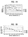
- Fig. 7A shows the contact resistance ( ⁇ ) of each resistor based on the comparative example with the sliding contact
- Fig. 7B shows the total resistance value (k ⁇ ) of the resistor based on the comparative example with the electrodes 3 and 4.
- the sliding element 5 is formed of a phosphor bronze plate having a silver-plated surface, and the contact part 5a of the sliding contact 5 is formed so as to be capable of crossing the whole length of the width dimension of 2.7 mm.
- the sliding contact 5 is slid at a speed of 20 mm/sec, and at this time, DC 5V is applied to the electrodes 3 and 4 from a DC power supply circuit 21, so that a constant current 10 (1 mA) is carried to the resistor 1 and the sliding contact 5.
- the voltage between the electrode 3 and the sliding contact 5 is measured when the sliding contact 5 is slid on the resistor 1, the change of resistance value is read from this voltage and the current I0, and the resistance value of the resistor 1 (the resistance value of the resistor 1 from the electrode 3 to the sliding contact 5) and the resistance value of the sliding contact 5 at respective points of time are subtracted to obtain the contact resistance ( ⁇ ).
- the maximum value of the contact resistance in the sliding of the sliding contact 5 is plotted in Figs. 6A and 7A.
- the contact resistance can be minimized, and the total resistance can be kept large if the drying time is 5 minutes or more and the drying temperature is not higher than the boiling point of the good solvent and not lower than the boiling point of the poor solvent, preferably, the vicinity of the intermediate temperature between the boiling points of both the solvents.
- the contact resistance of the surface of the resistor with the sliding contact or contact member can be reduced, and the total resistance can be also prevented from significantly lowering.
- the resistance value of the resistor can be precisely read.
Landscapes
- Engineering & Computer Science (AREA)
- Microelectronics & Electronic Packaging (AREA)
- Manufacturing & Machinery (AREA)
- Apparatuses And Processes For Manufacturing Resistors (AREA)
- Non-Adjustable Resistors (AREA)
- Adjustable Resistors (AREA)
Abstract
Description


Claims (9)
- A resistor formed of a conductive resin material comprising a binder resin and a conductive filler mixed to the binder resin, wherein when compared between a surface of the resistor and an internal cross section parallel to the surface of the resistor on the basis of regions partitioned in the same area, dispersity of the conductive filler in the binder resin is lower in the surface than in the cross section.
- The resistor according to claim 1, wherein a maximum dimension of two or more aggregates of the conductive filler is larger in the surface than in the cross section, when compared on the basis of the partitioned regions.
- The resistor according to claim 1 or 2, wherein a maximum diameter of two or more virtual circles drawable in a part free from the conductive filler is larger in the surface than in the cross section, when compared on the basis of the partitioned regions.
- A method for producing a resistor comprising:a process for printing, in a prescribed pattern, a mixed solution containing a good solvent having high solubility to a binder resin, a poor solvent lower in solubility than the good solvent and lower in volatility than the good solvent, a thermosetting binder resin, and a conductive filler;a process for drying the mixed solution; anda process for curing the binder resin by baking.
- The method for producing a resistor according to claim 4, wherein a boiling point of the poor solvent is higher than that of the good solvent.
- The method for producing a resistor according to claim 5, wherein a difference between both the boiling points is 15 °C or higher and 30 °C or lower.
- The method for producing a resistor according to claim 5 or 6, wherein the drying process is carried out at a temperature higher than the boiling point of the good solvent and lower than the boiling point of the poor solvent.
- The method for producing a resistor according to any of claims 4 to 7, wherein the good solvent is at least one or more of dipropylene glycol monomethyl ether, diethylene glycol monomethyl ether, diethylene glycol monoethyl ether, and dipropylene glycol monoethyl ether.
- The method for producing a resistor according to any of claims 4 to 8, wherein the poor solvent is at least one or more of terpineol, 2-phenoxy ethanol, and 2-benzyloxy ethanol.
Applications Claiming Priority (2)
| Application Number | Priority Date | Filing Date | Title |
|---|---|---|---|
| JP2002116956 | 2002-04-19 | ||
| JP2002116956A JP4139126B2 (en) | 2002-04-19 | 2002-04-19 | Resistor manufacturing method |
Publications (3)
| Publication Number | Publication Date |
|---|---|
| EP1355326A2 true EP1355326A2 (en) | 2003-10-22 |
| EP1355326A3 EP1355326A3 (en) | 2005-01-05 |
| EP1355326B1 EP1355326B1 (en) | 2006-05-31 |
Family
ID=28672672
Family Applications (1)
| Application Number | Title | Priority Date | Filing Date |
|---|---|---|---|
| EP03009011A Expired - Lifetime EP1355326B1 (en) | 2002-04-19 | 2003-04-17 | Method for producing a resistor |
Country Status (4)
| Country | Link |
|---|---|
| US (1) | US6787182B2 (en) |
| EP (1) | EP1355326B1 (en) |
| JP (1) | JP4139126B2 (en) |
| DE (1) | DE60305569T2 (en) |
Cited By (1)
| Publication number | Priority date | Publication date | Assignee | Title |
|---|---|---|---|---|
| DE102008012046A1 (en) * | 2008-03-01 | 2009-09-03 | Wincor Nixdorf International Gmbh | Device for level measurement in valuable containers |
Families Citing this family (2)
| Publication number | Priority date | Publication date | Assignee | Title |
|---|---|---|---|---|
| US7372127B2 (en) | 2001-02-15 | 2008-05-13 | Integral Technologies, Inc. | Low cost and versatile resistors manufactured from conductive loaded resin-based materials |
| KR102071763B1 (en) * | 2014-02-21 | 2020-01-30 | 미쓰이금속광업주식회사 | Copper-clad laminate for forming integrated capacitor layer, multilayer printed wiring board, and production method for multilayer printed wiring board |
Family Cites Families (5)
| Publication number | Priority date | Publication date | Assignee | Title |
|---|---|---|---|---|
| US4070200A (en) * | 1976-04-12 | 1978-01-24 | E. I. Du Pont De Nemours And Company | Compositions containing diethylene glycol ether |
| DE3145583A1 (en) * | 1981-11-17 | 1983-05-26 | Robert Bosch Gmbh, 7000 Stuttgart | PASTE FOR PRINTING SUBSTATES BY MEANS OF AN ELASTICALLY DEFORMABLE STAMP |
| JP2889792B2 (en) * | 1993-07-01 | 1999-05-10 | アルプス電気株式会社 | Variable resistor |
| US6083426A (en) * | 1998-06-12 | 2000-07-04 | Matsushita Electric Industrial Co., Ltd. | Conductive paste |
| JP3587730B2 (en) | 1999-05-25 | 2004-11-10 | アルプス電気株式会社 | Resistor and variable resistor using the resistor |
-
2002
- 2002-04-19 JP JP2002116956A patent/JP4139126B2/en not_active Expired - Fee Related
-
2003
- 2003-04-11 US US10/411,723 patent/US6787182B2/en not_active Expired - Fee Related
- 2003-04-17 EP EP03009011A patent/EP1355326B1/en not_active Expired - Lifetime
- 2003-04-17 DE DE60305569T patent/DE60305569T2/en not_active Expired - Fee Related
Cited By (1)
| Publication number | Priority date | Publication date | Assignee | Title |
|---|---|---|---|---|
| DE102008012046A1 (en) * | 2008-03-01 | 2009-09-03 | Wincor Nixdorf International Gmbh | Device for level measurement in valuable containers |
Also Published As
| Publication number | Publication date |
|---|---|
| JP4139126B2 (en) | 2008-08-27 |
| US6787182B2 (en) | 2004-09-07 |
| JP2003318003A (en) | 2003-11-07 |
| US20030197589A1 (en) | 2003-10-23 |
| DE60305569T2 (en) | 2007-05-03 |
| DE60305569D1 (en) | 2006-07-06 |
| EP1355326B1 (en) | 2006-05-31 |
| EP1355326A3 (en) | 2005-01-05 |
Similar Documents
| Publication | Publication Date | Title |
|---|---|---|
| US20080241390A1 (en) | Insulating polymers containing polyaniline and carbon nanotubes | |
| JPH06196304A (en) | Composition of polymer thick-film resistor | |
| JP2005171215A (en) | Electrically conductive polymer composition containing zirconia for coating, used for highly abrasion resistant film | |
| CN104916379B (en) | Conductive thin films containing silicon-carbon composites as printable thermistors | |
| CN110677985A (en) | Carbon film printed board high-conductivity paste resistance value regulation and control method | |
| US4036786A (en) | Fluorinated carbon composition and resistor utilizing same | |
| KR20150095406A (en) | Printable high heat resistance heating paste composition | |
| EP1355326B1 (en) | Method for producing a resistor | |
| TW201932529A (en) | Resin composition for forming varistor and varistor | |
| CN1339847A (en) | High frequency magnetic material and high frequency circuit element | |
| US5036027A (en) | Resistive paste and resistor material therefor | |
| JP3299083B2 (en) | Method for producing carbon-based conductive paste | |
| KR100418449B1 (en) | Resistor and variable resistor using the same | |
| KR100340482B1 (en) | Resistant material and variable resistor using the same | |
| JPH11251105A (en) | Thick-film resistance paste and its manufacture | |
| JP2014203652A (en) | Polymer type conductive paste and method of producing electrode by using the same | |
| KR100795571B1 (en) | Thick Film Resistor Paste, Manufacturing Method Thereof and Thick Film Resistor | |
| JP3605148B2 (en) | Thick film resistor composition and variable resistor | |
| US7307508B2 (en) | Sliding resistor having excellent sliding durability | |
| JP2000068106A (en) | Conductive paste | |
| JP4342270B2 (en) | Resistance pattern for electric circuit | |
| JPH11265809A (en) | Sliding resistor and manufacture of the same | |
| Hsu et al. | Silver particle carbon-matrix composites as thick films for electrical applications | |
| JP3972523B2 (en) | Carbon paste | |
| JP3767631B2 (en) | Method for adjusting resistance value of conductive film |
Legal Events
| Date | Code | Title | Description |
|---|---|---|---|
| PUAI | Public reference made under article 153(3) epc to a published international application that has entered the european phase |
Free format text: ORIGINAL CODE: 0009012 |
|
| AK | Designated contracting states |
Kind code of ref document: A2 Designated state(s): AT BE BG CH CY CZ DE DK EE ES FI FR GB GR HU IE IT LI LU MC NL PT RO SE SI SK TR |
|
| AX | Request for extension of the european patent |
Extension state: AL LT LV MK |
|
| PUAL | Search report despatched |
Free format text: ORIGINAL CODE: 0009013 |
|
| AK | Designated contracting states |
Kind code of ref document: A3 Designated state(s): AT BE BG CH CY CZ DE DK EE ES FI FR GB GR HU IE IT LI LU MC NL PT RO SE SI SK TR |
|
| AX | Request for extension of the european patent |
Extension state: AL LT LV MK |
|
| RIC1 | Information provided on ipc code assigned before grant |
Ipc: 7H 01C 10/30 B Ipc: 7H 01C 10/30 A Ipc: 7H 01C 17/065 B |
|
| 17P | Request for examination filed |
Effective date: 20050204 |
|
| 17Q | First examination report despatched |
Effective date: 20050301 |
|
| GRAP | Despatch of communication of intention to grant a patent |
Free format text: ORIGINAL CODE: EPIDOSNIGR1 |
|
| RTI1 | Title (correction) |
Free format text: METHOD FOR PRODUCING A RESISTOR |
|
| AKX | Designation fees paid |
Designated state(s): DE FR GB |
|
| GRAS | Grant fee paid |
Free format text: ORIGINAL CODE: EPIDOSNIGR3 |
|
| GRAA | (expected) grant |
Free format text: ORIGINAL CODE: 0009210 |
|
| AK | Designated contracting states |
Kind code of ref document: B1 Designated state(s): DE FR GB |
|
| REG | Reference to a national code |
Ref country code: GB Ref legal event code: FG4D |
|
| REF | Corresponds to: |
Ref document number: 60305569 Country of ref document: DE Date of ref document: 20060706 Kind code of ref document: P |
|
| ET | Fr: translation filed | ||
| PLBE | No opposition filed within time limit |
Free format text: ORIGINAL CODE: 0009261 |
|
| STAA | Information on the status of an ep patent application or granted ep patent |
Free format text: STATUS: NO OPPOSITION FILED WITHIN TIME LIMIT |
|
| 26N | No opposition filed |
Effective date: 20070301 |
|
| PGFP | Annual fee paid to national office [announced via postgrant information from national office to epo] |
Ref country code: GB Payment date: 20090312 Year of fee payment: 7 |
|
| PGFP | Annual fee paid to national office [announced via postgrant information from national office to epo] |
Ref country code: DE Payment date: 20090430 Year of fee payment: 7 Ref country code: FR Payment date: 20090406 Year of fee payment: 7 |
|
| GBPC | Gb: european patent ceased through non-payment of renewal fee |
Effective date: 20100417 |
|
| REG | Reference to a national code |
Ref country code: FR Ref legal event code: ST Effective date: 20101230 |
|
| PG25 | Lapsed in a contracting state [announced via postgrant information from national office to epo] |
Ref country code: DE Free format text: LAPSE BECAUSE OF NON-PAYMENT OF DUE FEES Effective date: 20101103 |
|
| PG25 | Lapsed in a contracting state [announced via postgrant information from national office to epo] |
Ref country code: GB Free format text: LAPSE BECAUSE OF NON-PAYMENT OF DUE FEES Effective date: 20100417 |
|
| PG25 | Lapsed in a contracting state [announced via postgrant information from national office to epo] |
Ref country code: FR Free format text: LAPSE BECAUSE OF NON-PAYMENT OF DUE FEES Effective date: 20100430 |