EP1355280A2 - Vibrator controlling circuit - Google Patents
Vibrator controlling circuit Download PDFInfo
- Publication number
- EP1355280A2 EP1355280A2 EP03009001A EP03009001A EP1355280A2 EP 1355280 A2 EP1355280 A2 EP 1355280A2 EP 03009001 A EP03009001 A EP 03009001A EP 03009001 A EP03009001 A EP 03009001A EP 1355280 A2 EP1355280 A2 EP 1355280A2
- Authority
- EP
- European Patent Office
- Prior art keywords
- signal
- spring
- vibrator
- integrated circuit
- control integrated
- Prior art date
- Legal status (The legal status is an assumption and is not a legal conclusion. Google has not performed a legal analysis and makes no representation as to the accuracy of the status listed.)
- Granted
Links
Images
Classifications
-
- B—PERFORMING OPERATIONS; TRANSPORTING
- B06—GENERATING OR TRANSMITTING MECHANICAL VIBRATIONS IN GENERAL
- B06B—METHODS OR APPARATUS FOR GENERATING OR TRANSMITTING MECHANICAL VIBRATIONS OF INFRASONIC, SONIC, OR ULTRASONIC FREQUENCY, e.g. FOR PERFORMING MECHANICAL WORK IN GENERAL
- B06B1/00—Methods or apparatus for generating mechanical vibrations of infrasonic, sonic, or ultrasonic frequency
- B06B1/02—Methods or apparatus for generating mechanical vibrations of infrasonic, sonic, or ultrasonic frequency making use of electrical energy
- B06B1/0207—Driving circuits
- B06B1/0223—Driving circuits for generating signals continuous in time
- B06B1/023—Driving circuits for generating signals continuous in time and stepped in amplitude, e.g. square wave, 2-level signal
Definitions
- This invention relates to a vibrator controlling circuit which is used in a portable telephone to notify a user of an incoming call.
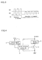
- Fig. 4 shows a conventional vibrator controlling circuit for vibrating a spring vibrator.
- a calling signal detection circuit 2 detects this calling signal and a power-supply voltage VDD is applied to a spring vibration control integrated circuit 3.
- Waveform (A) in Fig. 3 shows a square-wave signal used in the conventional vibrator controlling circuit of Fig. 4.
- a power-supply voltage VDD is applied to the spring vibration control integrated circuit 3
- a square-wave signal as shown in (A) is generated from the spring vibration control integrated circuit 3.
- This square-wave signal is applied to a gate electrode of an N-channel MOSFET 4.
- the N-channel MOSFET 4 repeats an ON/OFF operation in that the same is turned on every time a square-wave signal is applied and is turned off when it disappears, and an intermittent power-source voltage VDD is applied from a power source to a spring vibrator 5.
- Fig. 2 shows a spring vibrator 5 used in the conventional vibrator controlling circuit of Fig. 4.
- an electric current flows through a coil 6 of the spring vibrator 5, this coil 6 is magnetized due to electromagnetic induction.
- a magnet 9 in a leaf spring 8 provided on a substrate 7 is attracted.
- the square-wave signal applied to the gate electrode of the N-channel MOSFET 4 becomes low level, the N-channel MOSFET 4 is turned off, and the electric current to the coil 6 is intercepted.
- the spring vibrator 5 is restored by resilience of the leaf spring 8. By repeating such an operation, the spring vibrator 5 vibrates and gives notice of an incoming call.
- a power-source voltage VDD is applied to the spring vibration control integrated circuit 3
- the N-channel MOSFET 4 is turned on/off, and an intermittent electric current is supplied to the spring vibrator 5, whereby the spring vibrator 5 is vibrated to give notice of an incoming call.
- the invention provides a vibrator controlling circuit including a spring vibration control integrated circuit generating a first intermittent signal, a switching element performing an on and off operation based on the first intermittent signal applied by the spring vibration control integrated circuit, a spring vibrator vibrating based on the on and off operation of the switching element, and a cycle delaying signal generating circuit applying a delay signal to the spring vibration control integrated circuit when the vibration of the spring vibrator is forced to stop, whereby the spring vibration control integrated circuit applies to the switching element in response to the delay signal a second intermittent signal which is a reversal of the first intermittent signal.
- the invention also provides a vibrator controlling circuit including a spring vibration control integrated circuit generating a first square-wave signal when a calling signal is detected, a metal oxide semiconductor field effect transistor performing an on and off operation based on the first square-wave signal applied by the spring vibration control integrated circuit, a spring vibrator vibrating based on the on and off operation of the transistor, and a cycle delaying signal generating circuit applying a delay signal to the spring vibration control integrated circuit when the calling signal is not detected, the spring vibration control integrated circuit applies to the metal oxide semiconductor field effect transistor in response to the delay signal a second square-wave signal which has a phase shifted from a phase of the first square-wave signal.
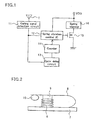
- Fig. 1 is a block diagram of the vibrator controlling circuit of this invention.
- a calling signal detection circuit 11 detects a calling signal received by an antenna T.
- a spring vibration control integrated circuit 12 receives a power-source voltage VDD and generates a square-wave signal when the calling signal is detected by the calling signal detection circuit 11.
- a cycle delaying circuit 13 generates a delaying signal when the calling signal from the calling signal detection circuit 11 is stopped.
- the delaying signal generated from the cycle delaying circuit 13 is applied for a fixed period via a counter 14 to the spring vibration control integrated circuit 12.
- the delaying signal is applied to the spring vibration control integrated circuit 12, if duty of the square-wave signal is 50%, a square-wave signal whose cycle is delayed by 1/2 compared to that in the vibrating operation is generated from the spring vibration control integrated circuit 12.
- An N-channel MOSFET 15 is ON for a period where a square-wave signal generated from the spring vibration control integrated circuit 12 is at high level, and is OFF for a period when it is at low level.
- a coil current intermittently flows every time the N-channel MOSFET 15 is turned on/off.
- the spring vibrator 16 includes a coil 6 which is attached on a substrate 7 and through which the intermittent coil current flows, a leaf spring 8 whose one end is provided on the substrate 7, and a weight 10 provided so that a magnet 9 provided on the leaf spring 8 and the leaf spring 8 appropriately vibrate.
- Fig. 3 compares a square-wave signal (B) of this embodiment to the square-wave signal (A) of the conventional device of Fig. 4.
- VDD power-source voltage
- the square-wave signal is a square-wave signal whose duty is 50% at 100Hz and is applied to a gate electrode of the N-channel MOSFET 15.
- the N-channel MOSFET 15 repeats an ON/OFF operation in that the same is turned on every time a square-wave signal becomes high level and is turned off when it becomes low level, and an intermittent coil current is applied from a power source to a spring vibrator 16.
- the spring vibrator 16 performs vibration based on detection of a calling signal
- a square-wave signal from the spring vibration control integrated circuit 12 when a square-wave signal from the spring vibration control integrated circuit 12 is high level, the N-channel MOSFET 15 is turned on, due to electromagnetic induction caused by the electric current that flows through the coil 6 provided on the substrate 7, an attracting effect works between the coil 6 and magnet 9, the leaf spring 8 is attracted toward the substrate 7 and approaches thereto, and when the square-wave signal is low level, the N-channel MOSFET 15 is turned off, an electric current to the coil 6 is interrupted, and the leaf spring 8 becomes distant from the substrate 8 by its own resilience.
- the N-channel MOSFET 15 is turned on and allows the coil current to flow to the coil 6. Therefore, since a force in a direction toward the substrate 7 works on the leaf spring 8 due to electromagnetic induction, the vibration of the leaf spring 8 is suppressed.
- the number of the vibrations of the leaf spring 8 between the cease of detecting the calling signal and the ending of the vibration thereafter is determined beforehand. This number is, for example, 1-20.
- the counter 14 counts the number of delaying signals from the cycle delaying signal generating circuit 13, and the operation of the cycle delaying signal generating circuit 13 stops when the counted number reaches the predetermined number.
Landscapes
- Engineering & Computer Science (AREA)
- Mechanical Engineering (AREA)
- Mobile Radio Communication Systems (AREA)
- Apparatuses For Generation Of Mechanical Vibrations (AREA)
- Reciprocating, Oscillating Or Vibrating Motors (AREA)
- Electrostatic, Electromagnetic, Magneto- Strictive, And Variable-Resistance Transducers (AREA)
Abstract
Description
Claims (3)
- A vibrator controlling circuit comprising:a spring vibration control integrated circuit (12) generating a first intermittent signal;a switching element (15) performing an on and off operation based on the first intermittent signal applied by the spring vibration control integrated circuit (12);a spring vibrator (16) vibrating based on the on and off operation of the switching element (15); anda cycle delaying signal generating circuit (13) applying a delay signal to the spring vibration control integrated circuit (12) when the vibration of the spring vibrator (16) is forced to stop, the spring vibration control integrated circuit (12) applying to the switching element (15) in response to the delay signal a second intermittent signal which is a reversal of the first intermittent signal.
- A vibrator controlling circuit comprising:a spring vibration control integrated circuit (12) generating a first square-wave signal when a calling signal is detected;a metal oxide semiconductor field effect transistor (15) performing an on and off operation based on the first square-wave signal applied by the spring vibration control integrated circuit (12);a spring vibrator (16) vibrating based on the on and off operation of the transistor (15); anda cycle delaying signal generating circuit (13) applying a delay signal to the spring vibration control integrated circuit (12) when the calling signal is not detected, the spring vibration control integrated circuit (12) applying to the metal oxide semiconductor field effect transistor in response to the delay signal a second square-wave signal which has a phase shifted from a phase of the first square-wave signal.
- The vibrator controlling circuit of claim 2, further comprising a counter circuit (14) counting the number of the delay signals applied by the cycle delaying signal generating circuit (13) to the spring vibration control integrated circuit (12), wherein the cycle delaying signal generating circuit (13) stops the application of the delay signal when the counted number of the delay signals reaches a predetermined number.
Applications Claiming Priority (2)
| Application Number | Priority Date | Filing Date | Title |
|---|---|---|---|
| JP2002114958 | 2002-04-17 | ||
| JP2002114958A JP2003309897A (en) | 2002-04-17 | 2002-04-17 | Vibrator control circuit |
Publications (3)
| Publication Number | Publication Date |
|---|---|
| EP1355280A2 true EP1355280A2 (en) | 2003-10-22 |
| EP1355280A3 EP1355280A3 (en) | 2004-03-24 |
| EP1355280B1 EP1355280B1 (en) | 2006-06-28 |
Family
ID=28672644
Family Applications (1)
| Application Number | Title | Priority Date | Filing Date |
|---|---|---|---|
| EP03009001A Expired - Lifetime EP1355280B1 (en) | 2002-04-17 | 2003-04-17 | Vibrator controlling circuit |
Country Status (5)
| Country | Link |
|---|---|
| US (1) | US6831428B2 (en) |
| EP (1) | EP1355280B1 (en) |
| JP (1) | JP2003309897A (en) |
| CN (1) | CN100377479C (en) |
| DE (1) | DE60306445D1 (en) |
Families Citing this family (5)
| Publication number | Priority date | Publication date | Assignee | Title |
|---|---|---|---|---|
| JPWO2009141970A1 (en) | 2008-05-19 | 2011-09-29 | 株式会社村田製作所 | Vibration device |
| WO2018131541A1 (en) * | 2017-01-13 | 2018-07-19 | ミツミ電機株式会社 | Vibratory actuator, wearable terminal, and incoming call notification function device |
| WO2018189914A1 (en) * | 2017-04-14 | 2018-10-18 | 富士通株式会社 | Tactile sensation presentation device and simulation system |
| KR101972860B1 (en) | 2017-06-30 | 2019-04-26 | 주식회사 엠플러스 | Linear Vibrator. |
| JP6955158B2 (en) * | 2017-11-17 | 2021-10-27 | ミツミ電機株式会社 | Vibration actuators and mobile devices |
Family Cites Families (5)
| Publication number | Priority date | Publication date | Assignee | Title |
|---|---|---|---|---|
| US5596311A (en) * | 1995-05-23 | 1997-01-21 | Preco, Inc. | Method and apparatus for driving a self-resonant acoustic transducer |
| DE69623427T2 (en) * | 1995-12-29 | 2003-05-22 | Ishida Co., Ltd. | Method and device for controlling vibratory conveyors |
| JP3674216B2 (en) * | 1997-02-25 | 2005-07-20 | 松下電工株式会社 | Drive control method for linear vibration motor |
| JP4077934B2 (en) * | 1998-06-30 | 2008-04-23 | キヤノン株式会社 | Vibration wave motor drive control method, vibration wave motor drive control apparatus, apparatus including vibration wave motor, and image forming apparatus |
| JP3545650B2 (en) * | 1999-07-27 | 2004-07-21 | 日本エイ・シィ・アール株式会社 | Electromagnetic device and its driving circuit |
-
2002
- 2002-04-17 JP JP2002114958A patent/JP2003309897A/en active Pending
-
2003
- 2003-04-15 US US10/413,582 patent/US6831428B2/en not_active Expired - Fee Related
- 2003-04-15 CN CNB031101747A patent/CN100377479C/en not_active Expired - Fee Related
- 2003-04-17 DE DE60306445T patent/DE60306445D1/en not_active Expired - Lifetime
- 2003-04-17 EP EP03009001A patent/EP1355280B1/en not_active Expired - Lifetime
Also Published As
| Publication number | Publication date |
|---|---|
| JP2003309897A (en) | 2003-10-31 |
| DE60306445D1 (en) | 2006-08-10 |
| CN1452303A (en) | 2003-10-29 |
| EP1355280A3 (en) | 2004-03-24 |
| US6831428B2 (en) | 2004-12-14 |
| EP1355280B1 (en) | 2006-06-28 |
| US20040124795A1 (en) | 2004-07-01 |
| CN100377479C (en) | 2008-03-26 |
Similar Documents
| Publication | Publication Date | Title |
|---|---|---|
| US5945772A (en) | Damped resonant piezoelectric alerting device | |
| US11659336B2 (en) | Vibration apparatus, mobile terminal and method for controlling the mobile terminal | |
| US6831428B2 (en) | Vibrator controlling circuit | |
| US20100052878A1 (en) | Vibrating apparatus of a portable electronic device | |
| CN108432217A (en) | a mobile terminal | |
| EP1220177B1 (en) | Vibrator controlling circuit | |
| JP2000165992A (en) | Electromagnetic transducer with good impact resistance | |
| US7035423B2 (en) | Mobile terminal with electromagnetic actuator | |
| TW487605B (en) | Vibration-generating device and portable telephone comprising the same | |
| US9546919B2 (en) | Electronic apparatus and shock detection method | |
| JPS59181004A (en) | Driving circuit for coil of electromagnet device | |
| JP2002300231A (en) | Incoming call notifying device, incoming call notifying method, and portable terminal | |
| US5635788A (en) | Control circuit for a piezoelectric vibrator | |
| JP3885927B2 (en) | Vibrator control circuit | |
| KR100376007B1 (en) | Self-excited vibration type vibration device with electromagnet | |
| JPH11313395A (en) | Electric vibration converter | |
| JP6219087B2 (en) | Electronic device, portable device, and control method of electronic device | |
| JP6863337B2 (en) | Pulse signal output circuit | |
| JP2002301431A (en) | Vibrator control circuit | |
| WO1999063604A1 (en) | Resonant piezoelectric alerting device | |
| JPS6110818A (en) | Drive circuit of electrostrictive actuator | |
| JP3274465B2 (en) | Circuits for generating control signals dependent on generation of extremes of sinusoidal oscillations and uses of such circuits | |
| JP2001326988A (en) | Driving circuit for electroacoustic transducer and driving method thereof | |
| JP2025086066A (en) | Vibration device and vibration method thereof | |
| JP2010193417A (en) | Apparatus for remote notification of vibrator start in cellular phone |
Legal Events
| Date | Code | Title | Description |
|---|---|---|---|
| PUAI | Public reference made under article 153(3) epc to a published international application that has entered the european phase |
Free format text: ORIGINAL CODE: 0009012 |
|
| AK | Designated contracting states |
Kind code of ref document: A2 Designated state(s): AT BE BG CH CY CZ DE DK EE ES FI FR GB GR HU IE IT LI LU MC NL PT RO SE SI SK TR |
|
| AX | Request for extension of the european patent |
Extension state: AL LT LV MK RO SI |
|
| PUAL | Search report despatched |
Free format text: ORIGINAL CODE: 0009013 |
|
| AK | Designated contracting states |
Kind code of ref document: A3 Designated state(s): AT BE BG CH CY CZ DE DK EE ES FI FR GB GR HU IE IT LI LU MC NL PT RO SE SI SK TR |
|
| AX | Request for extension of the european patent |
Extension state: AL LT LV MK RO SI |
|
| RIC1 | Information provided on ipc code assigned before grant |
Ipc: 7G 08B 6/00 A Ipc: 7B 06B 1/02 B |
|
| 17P | Request for examination filed |
Effective date: 20040923 |
|
| AKX | Designation fees paid |
Designated state(s): DE FI FR GB |
|
| 17Q | First examination report despatched |
Effective date: 20050609 |
|
| GRAP | Despatch of communication of intention to grant a patent |
Free format text: ORIGINAL CODE: EPIDOSNIGR1 |
|
| GRAS | Grant fee paid |
Free format text: ORIGINAL CODE: EPIDOSNIGR3 |
|
| GRAA | (expected) grant |
Free format text: ORIGINAL CODE: 0009210 |
|
| AK | Designated contracting states |
Kind code of ref document: B1 Designated state(s): DE FI FR GB |
|
| REG | Reference to a national code |
Ref country code: GB Ref legal event code: FG4D |
|
| REF | Corresponds to: |
Ref document number: 60306445 Country of ref document: DE Date of ref document: 20060810 Kind code of ref document: P |
|
| PG25 | Lapsed in a contracting state [announced via postgrant information from national office to epo] |
Ref country code: DE Free format text: LAPSE BECAUSE OF FAILURE TO SUBMIT A TRANSLATION OF THE DESCRIPTION OR TO PAY THE FEE WITHIN THE PRESCRIBED TIME-LIMIT Effective date: 20060929 |
|
| PLBE | No opposition filed within time limit |
Free format text: ORIGINAL CODE: 0009261 |
|
| STAA | Information on the status of an ep patent application or granted ep patent |
Free format text: STATUS: NO OPPOSITION FILED WITHIN TIME LIMIT |
|
| EN | Fr: translation not filed | ||
| 26N | No opposition filed |
Effective date: 20070329 |
|
| GBPC | Gb: european patent ceased through non-payment of renewal fee |
Effective date: 20070417 |
|
| PG25 | Lapsed in a contracting state [announced via postgrant information from national office to epo] |
Ref country code: GB Free format text: LAPSE BECAUSE OF NON-PAYMENT OF DUE FEES Effective date: 20070417 Ref country code: FR Free format text: LAPSE BECAUSE OF FAILURE TO SUBMIT A TRANSLATION OF THE DESCRIPTION OR TO PAY THE FEE WITHIN THE PRESCRIBED TIME-LIMIT Effective date: 20070511 |
|
| PGFP | Annual fee paid to national office [announced via postgrant information from national office to epo] |
Ref country code: FI Payment date: 20080411 Year of fee payment: 6 |
|
| PG25 | Lapsed in a contracting state [announced via postgrant information from national office to epo] |
Ref country code: FR Free format text: LAPSE BECAUSE OF FAILURE TO SUBMIT A TRANSLATION OF THE DESCRIPTION OR TO PAY THE FEE WITHIN THE PRESCRIBED TIME-LIMIT Effective date: 20060628 |
|
| PG25 | Lapsed in a contracting state [announced via postgrant information from national office to epo] |
Ref country code: FI Free format text: LAPSE BECAUSE OF NON-PAYMENT OF DUE FEES Effective date: 20090417 |