EP1353216A1 - Lcd device and lcd panel - Google Patents
Lcd device and lcd panel Download PDFInfo
- Publication number
- EP1353216A1 EP1353216A1 EP01900766A EP01900766A EP1353216A1 EP 1353216 A1 EP1353216 A1 EP 1353216A1 EP 01900766 A EP01900766 A EP 01900766A EP 01900766 A EP01900766 A EP 01900766A EP 1353216 A1 EP1353216 A1 EP 1353216A1
- Authority
- EP
- European Patent Office
- Prior art keywords
- liquid crystal
- crystal panel
- substrate
- emitting surface
- display device
- Prior art date
- Legal status (The legal status is an assumption and is not a legal conclusion. Google has not performed a legal analysis and makes no representation as to the accuracy of the status listed.)
- Withdrawn
Links
Images




Classifications
-
- G—PHYSICS
- G02—OPTICS
- G02F—OPTICAL DEVICES OR ARRANGEMENTS FOR THE CONTROL OF LIGHT BY MODIFICATION OF THE OPTICAL PROPERTIES OF THE MEDIA OF THE ELEMENTS INVOLVED THEREIN; NON-LINEAR OPTICS; FREQUENCY-CHANGING OF LIGHT; OPTICAL LOGIC ELEMENTS; OPTICAL ANALOGUE/DIGITAL CONVERTERS
- G02F1/00—Devices or arrangements for the control of the intensity, colour, phase, polarisation or direction of light arriving from an independent light source, e.g. switching, gating or modulating; Non-linear optics
- G02F1/01—Devices or arrangements for the control of the intensity, colour, phase, polarisation or direction of light arriving from an independent light source, e.g. switching, gating or modulating; Non-linear optics for the control of the intensity, phase, polarisation or colour
- G02F1/13—Devices or arrangements for the control of the intensity, colour, phase, polarisation or direction of light arriving from an independent light source, e.g. switching, gating or modulating; Non-linear optics for the control of the intensity, phase, polarisation or colour based on liquid crystals, e.g. single liquid crystal display cells
- G02F1/133—Constructional arrangements; Operation of liquid crystal cells; Circuit arrangements
- G02F1/1333—Constructional arrangements; Manufacturing methods
- G02F1/1335—Structural association of cells with optical devices, e.g. polarisers or reflectors
- G02F1/133504—Diffusing, scattering, diffracting elements
-
- G—PHYSICS
- G02—OPTICS
- G02F—OPTICAL DEVICES OR ARRANGEMENTS FOR THE CONTROL OF LIGHT BY MODIFICATION OF THE OPTICAL PROPERTIES OF THE MEDIA OF THE ELEMENTS INVOLVED THEREIN; NON-LINEAR OPTICS; FREQUENCY-CHANGING OF LIGHT; OPTICAL LOGIC ELEMENTS; OPTICAL ANALOGUE/DIGITAL CONVERTERS
- G02F1/00—Devices or arrangements for the control of the intensity, colour, phase, polarisation or direction of light arriving from an independent light source, e.g. switching, gating or modulating; Non-linear optics
- G02F1/01—Devices or arrangements for the control of the intensity, colour, phase, polarisation or direction of light arriving from an independent light source, e.g. switching, gating or modulating; Non-linear optics for the control of the intensity, phase, polarisation or colour
- G02F1/13—Devices or arrangements for the control of the intensity, colour, phase, polarisation or direction of light arriving from an independent light source, e.g. switching, gating or modulating; Non-linear optics for the control of the intensity, phase, polarisation or colour based on liquid crystals, e.g. single liquid crystal display cells
- G02F1/133—Constructional arrangements; Operation of liquid crystal cells; Circuit arrangements
- G02F1/136—Liquid crystal cells structurally associated with a semi-conducting layer or substrate, e.g. cells forming part of an integrated circuit
- G02F1/1362—Active matrix addressed cells
- G02F1/1368—Active matrix addressed cells in which the switching element is a three-electrode device
Definitions
- the present invention relates to a liquid crystal display device and a liquid crystal panel and, more particularly, to a liquid crystal display device and a liquid crystal panel that can prevent a degradation of display quality.
- Fig. 11 schematically shows a conventional mobile phone.
- Fig. 12 schematically shows a part of a cross section taken along the line XII-XII in Fig. 11.
- Fig. 13 schematically shows a cross section of a liquid crystal panel used in the mobile phone shown in Fig. 12.
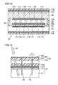
- Fig. 14 is a schematic cross-sectional view showing a mechanism of displaying an image or the like on an LCD portion 102 of the mobile phone shown in Figs. 11-13.
- a conventional mobile phone 101 includes an LCD (Liquid Crystal Display) portion 102, a receiver located on an upper portion of a body of mobile phone 101, a microphone located on a lower portion of the body, and an input portion for an input operation.
- the receiver transmits to a user a voice of a person the user is speaking to.
- the microphone is used for a voice input by a user.
- LCD portion 102 is for a variable display of any kind of information, for example, text information such as a list of telephone numbers or an e-mail, or video information such as an image.
- an antenna is located on the upper portion of the body.
- a liquid crystal panel 107 is used in LCD portion 102, as shown in Fig. 12.
- Liquid crystal panel 107 is held in a casing of mobile phone 101 formed of a front case 106 and a rear case (not shown).
- An opening is formed in front case 106 in a region above an emitting surface of liquid crystal panel 107 from which light is emitted.
- An in-molded part 103 is arranged to cover the opening.
- In-molded part 103 is formed of a plastic molded part 105 and an in-mold film 104 arranged on a surface of plastic molded part 105.
- In-mold film 104 is a multilayer film and, as shown in Fig.
- In-molded part 103 is produced with a so-called in-mold method. This is a method to produce an in-molded part which is an integrated product of plastic molded part 105 and in-mold film 104 by one shot, through the step of setting an in-mold film for the purpose of, for example, decoration or function enhancement inside a mold used for plastic molding upon a plastic molding process, and then performing a plastic molding process.
- Such in-molded part 103 is adopted as means for enhancing a degree of freedom in designing mobile phone 101 while preventing an increase in a production cost.
- An active matrix type liquid crystal panel has come to be used as liquid crystal panel 107 to obtain high display quality.
- An exemplary structure of such active matrix type liquid crystal panel 107 will be described with reference to Fig. 13.
- liquid crystal panel 107 is a semipermeable type color liquid crystal panel.
- a substrate 108 of a transparent material such as glass having an element such as a thin film field effect transistor, a switching element for controlling a display at each pixel of a liquid crystal, formed on its surface and a CF (Color Filter) substrate 109 having color filters 115a-115c arranged on a surface thereof, are arranged opposite to each other to sandwich a liquid crystal 142 therebetween.
- Data lines 110a-110c which are conductive lines for controlling the switching element, and transparent electrodes 111a-111c for applying an electric field to liquid crystal 142 are arranged on a surface of substrate 108 that faces liquid crystal 142.
- An orientation film 112a is formed on surfaces of data lines 110a-110c and transparent electrodes 111a-111c that face liquid crystal 142.
- a reflection film 116 for reflecting light incoming from an emitting surface of liquid crystal panel 107 is formed on a surface of CF substrate 109 that faces liquid crystal 142.
- Color filters 115a-115c are arranged on reflection film 116.
- Color filters 115a-115c are the filters of red, green and blue colors, respectively.
- An overcoat film 114 is arranged on color filters 115a-115c.
- a transparent electrode 113 as an opposite electrode is arranged on overcoat film 114.
- An orientation film 112b is arranged on transparent electrode 113.
- Liquid crystal 142 is held between orientation films 112a and 112b.
- a seal material for holding liquid crystal 142 is arranged between substrate 108 and CF substrate 109.
- phase difference plate ( ⁇ /4 plate) 117a is fixed on a surface of the emitting surface side of the substrate in liquid crystal panel 107 with an adhesion layer 119 interposed therebetween.
- a polarizer 118a is arranged on phase difference plate 117a.
- a phase difference plate ( ⁇ /4 plate) 117b is fixed on that surface of CF substrate 109, which is opposite to the surface facing liquid crystal 142, with an adhesion layer (not shown) interposed therebetween.
- a polarizer 118b is arranged on that surface of phase difference plate 117b which is opposite to the surface facing CF substrate 109.
- an incident light 125 which enters liquid crystal panel 107 via in-molded part 103 comes into liquid crystal panel 107 from an emitting surface of liquid crystal panel 107 (a surface facing to in-molded part 103).
- Incident light 125 is then reflected by reflection film 116 on a substrate portion 121 of liquid crystal panel 107.
- the reflected light (reflected light 126) proceeds from substrate portion 121 through adhesion layer 119, phase difference plate 117a and polarizer 118a, and is emitted from the emitting surface of liquid crystal panel 107.
- Reflected light 126 then exits the LCD portion of mobile phone 101 via in-molded part 103. Reflected light 126 is colored by color filters 115a-115c.
- an optical property of liquid crystal 142 can vary by altering a potential of each of transparent electrodes 111a-111c by the switching element to modify an intensity, a direction or the like of an electric field applied to liquid crystal 142. As a result, it is possible to switch between the states transmitting and not transmitting reflected light 126 of liquid crystal 142. Therefore, by controlling the switching element corresponding to each pixel so as to display a prescribed character or image, a prescribed character or image can be displayed on LCD portion 102.
- a purpose of the present invention is to provide a liquid crystal display device and a liquid crystal panel which can improve the display property.
- the inventor accomplished the present invention by studying and finding a cause of the above-described glare generation.
- the inventor thoroughly examined a structure of a mobile phone as a liquid crystal display device generating a glare.
- a very small inequality formed on peel layer 123 of in-mold film 104 constructing in-molded part 103 of mobile phone 101 was found as shown in Fig. 14.
- a pitch P1 of this inequality was approximately 0.2 mm to 0.4 mm. It is probable that this inequality of peel layer 123 was formed by a transfer of an inequality shape formed on a surface of a drum around which in-mold film 104 was coiled during a photogravure of in-mold film 104 prior to perform the in-mold method.
- a pitch of the pixels of liquid crystal panel 107 is now approximately 0.2 mm to 0.3 mm to attain a high resolution of liquid crystal panel 107.
- reflected light 126 from liquid crystal panel 107 has an intensity distribution with a pitch corresponding to the pitch of the pixels. Therefore, the pitch of the intensity distribution of reflected light 126 will be nearly the same size as the pitch P1 of the inequality of peel layer 123.
- the glare is generated by an interference of the inequality of peel layer 123 of in-mold film 104 with reflected light 126 (that is, the glare is regarded as an unevenness of an interference of reflected light 126 with the inequality of peel layer 123.)
- a liquid crystal display device in accordance with one aspect of the present invention includes an active matrix type liquid crystal panel holding liquid crystal, a window member located on the liquid crystal panel and transmitting light emitted from the liquid crystal panel, and a diffusion member located between the liquid crystal of the liquid crystal panel and the window member and diffusing light emitted from the liquid crystal.
- the light emitted from the liquid crystal panel has an intensity distribution corresponding to the pixel pitch of the liquid crystal panel.
- a leveling of the intensity distribution corresponding to the pixel pitch of the liquid crystal panel is possible for the light emitted from the liquid crystal panel.
- an inequality with a pitch similar to the pixel pitch is formed in a light transmitting portion of the window member (if, for example, an inequality with a pitch similar to the pixel pitch is formed on an in-mold film constructing an in-molded part when the in-molded part or the like is used as the window member)
- an interference of the light emitted from the liquid crystal panel with the inequality formed on the window member as mentioned above can be suppressed. Therefore, as the generation of the so-called glare can be prevented, degradation of display quality of the liquid crystal display device can be prevented.
- the generation of the glare can also be prevented by using an in-molded part or the like for the window member as mentioned above. Therefore, the degree of freedom in designing a liquid crystal display device can be enhanced while keeping high display quality of the liquid crystal display device by applying the in-molded part or the like to the window member.
- the diffusion member includes a base material which can transmit light, and a light diffusion material which is arranged dispersed in the base material.
- a light diffusion property of the diffusion member can be changed arbitrarily by modifying a size of the light diffusion material dispersed in the base material and a distribution density of the light diffusion material in the base material.
- an optical property of the diffusion member can be set to diffuse the light emitted from the liquid crystal panel so as to decrease the glare without significantly degrading the high display quality of the active matrix type liquid crystal panel.
- the liquid crystal panel includes first and second substrates holding the liquid crystal.
- the first substrate may be located on the emitting surface side of the liquid crystal panel that emits light, while the second substrate may be located in a region at a larger distance from the emitting surface than the first substrate when seen from the liquid crystal.
- the liquid crystal panel may include an optical member arranged on that surface of the first substrate which is opposite to the surface facing the liquid crystal.
- the diffusion member may be located between the first substrate and the optical member.
- the diffusion member can be integrated in the liquid crystal panel.
- a liquid crystal display device formed of members such as a liquid crystal panel and a casing integrating the liquid crystal panel it is unnecessary to significantly modify the design of the members other than the liquid crystal panel, such as the casing. Therefore, by using the liquid crystal panel having the diffusion member, the design of the members, such as the casing, of the conventional liquid crystal display device can easily be applied to the liquid crystal display device of the present invention. Consequently, a designing time period for the members such as the casing to realize the liquid crystal display device of the present invention can be shortened, so that the production cost of the liquid crystal display device of the present invention is not increased.
- the diffusion member is an adhesion layer that adheres the optical member to the first substrate.
- the adhesion layer that adheres the optical member to the first substrate also exists in the conventional liquid crystal panel.
- the shape of the liquid crystal panel similar to that of the conventional one can be attained by adding a function of a diffusion member to the existing adhesion layer.
- the designing cost to realize the liquid crystal display device of the present invention can further be decreased.
- a preferred haze value of the diffusion member is between 50 % and 60 %.
- a liquid crystal panel in accordance with another aspect of the present invention is an active matrix type liquid crystal panel holding liquid crystal, and includes first and second substrates holding liquid crystal.
- the first substrate is located on an emitting surface side of the liquid crystal panel that emits light, while the second substrate is located in a region at a larger distance from the emitting surface than the first substrate when seen from the liquid crystal.
- the liquid crystal panel includes an optical member arranged on that surface of the first substrate which is opposite to the surface facing the liquid crystal, and a diffusion member located between the first substrate and the optical member.
- the light emitted from the liquid crystal panel has an intensity distribution corresponding to the pixel pitch of the liquid crystal panel.
- a leveling of the intensity distribution corresponding to the pixel pitch of the liquid crystal panel is possible for the light emitted from the liquid crystal panel. Assuming that a window member or the like is arranged on the emitting surface of the liquid crystal panel.
- an inequality with a pitch similar to the pixel pitch is formed in a portion of the window member which transmits light emitted from the liquid crystal panel (if, for example, an inequality with a pitch similar to the pixel pitch is formed on an in-mold film constructing an in-molded part when the in-molded part or the like is used as the window member)
- an interference of the light emitted from the liquid crystal panel with the inequality formed on the window member can be suppressed because the intensity distribution of the emitted light is leveled. Therefore, as the generation of the so-called glare can be prevented, degradation of display quality of the liquid crystal panel can be prevented.
- the diffusion member includes a base material which can transmit light, and a light diffusion material which is arranged dispersed in the base material.
- a light diffusion property of the diffusion member can be changed arbitrarily by modifying a size of the light diffusion material dispersed in the base material and a distribution density of the light diffusion material in the base material.
- an optical property of the diffusion member can be set to diffuse the light emitted from the liquid crystal panel so as to decrease the glare without significantly degrading the high display quality of the active matrix type liquid crystal panel.
- the diffusion member is an adhesion layer that adheres the optical member to the first substrate.
- the adhesion layer that adheres the optical member to the first substrate also exists in the conventional liquid crystal panel.
- the shape of the liquid crystal panel similar to that of the conventional one can be attained by adding a function of a diffusion member to the existing adhesion layer.
- the designing cost to realize the liquid crystal display device using the liquid crystal panel according to the present invention can further be decreased.
- a preferred haze value of the diffusion member is between 50 % and 60 %.
- the haze value of the diffusion member is in the range mentioned above, an interference of the light emitted from the liquid crystal panel with the inequality formed on the window member can be prevented by appropriately diffusing the light emitted from the liquid crystal panel while maintaining the high display quality of the active matrix type liquid crystal panel, even if the window member having an inequality with a pitch similar to the pixel pitch of the liquid crystal panel formed thereon (such as the window member formed of an in-molded part having an in-mold film including an inequality) is arranged on the emitting surface of the liquid crystal panel.
- a liquid crystal display device in accordance with another aspect of the present invention includes an active matrix type liquid crystal panel, a frame member located on the liquid crystal panel and having an opening formed in a region located above an emitting surface of the liquid crystal panel which emits light, and a window member located to cover the opening of the frame member and transmitting light emitted from the emitting surface of the liquid crystal panel.
- the window member the region that transmits light emitted from the emitting surface of the liquid crystal panel is formed of a single layer of transparent material.
- the light emitted from the emitting surface of the liquid crystal panel has an intensity distribution corresponding to the pixel pitch of the liquid crystal panel.
- the region transmitting light emitted from the emitting surface of the liquid crystal panel is formed of a single layer of transparent material, the region does not have a multilayer structure as an in-molded part in which an in-mold film is arranged on a surface of a plastic molded part. Therefore, there is no phenomenon such as an interference of the inequality formed on the in-mold film with the light emitted from the emitting surface of the liquid crystal panel. This surely prevents the generation of the so-called glare. Thus, degradation of a display property of the liquid crystal display device by the glare can surely be prevented.
- the degree of freedom in designing the liquid crystal display device can be enhanced by arbitrarily changing the design of the frame member while keeping the good display property.
- a liquid crystal display device in accordance with another aspect of the present invention includes an active matrix type liquid crystal panel, a casing arranged to surround the liquid crystal panel and having an opening formed in a region facing an emitting surface of the liquid crystal panel which emits light, and a window member located to cover the opening of the casing and transmitting light emitted from the emitting surface of the liquid crystal panel.
- the window member the region that transmits light emitted from a display surface of the liquid crystal panel is formed of a single layer of transparent material.
- the light emitted from the emitting surface of the liquid crystal panel has an intensity distribution corresponding to the pixel pitch of the liquid crystal panel.
- the region transmitting light emitted from the emitting surface of the liquid crystal panel is formed of a single layer of transparent material, the region does not have a multilayer structure as an in-molded part in which an in-mold film is arranged on a surface of a plastic molded part. Therefore, there is no phenomenon such as an interference of the inequality formed on the in-mold film with the light emitted from the emitting surface of the liquid crystal panel. This surely prevents the generation of the so-called glare. Thus, degradation of a display property of the liquid crystal display device by the glare can be prevented.
- the window member may include a colored layer formed on a surface of a region other than the region that transmits light emitted from the display surface of the liquid crystal panel.
- an arbitrary design can be provided to the window member by forming the colored layer of an arbitrary color and form on the window member.
- FIG. 1 A first embodiment of a mobile phone according to the present invention will be described with reference to Figs. 1-4.
- a mobile phone 1 includes an LCD (Liquid Crystal Display) portion 2, a receiver located on an upper portion of a body of mobile phone 1, a microphone located on a lower portion of the body, and an input portion for an input operation.
- the receiver transmits to a user a voice of a person the user is speaking to.
- the microphone is used for a voice input by a user.
- LCD portion 2 is for a variable display of any kind of information, for example, text information such as a list of telephone numbers or an e-mail, or video information such as an image.
- an antenna is located on the upper portion of the body.
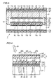
- a liquid crystal panel 7 is used in LCD portion 2, as shown in Fig. 2.
- Liquid crystal panel 7 is held in a casing of mobile phone 1 formed of a front case 6 and a rear case (not shown).
- An opening is formed in front case 6 in a region above an emitting surface of liquid crystal panel 7 from which light is emitted.
- An in-molded part 3 is arranged to cover the opening.
- In-molded part 3 is formed of a plastic molded part 5 and an in-mold film 4 arranged on a surface of plastic molded part 5.
- In-mold film 4 is a multilayer film and, as shown in Fig. 4, includes a peel layer 23 located on a surface of plastic molded part 5 and an in-mold film top layer 22 located on peel layer 23.
- In-mold film top layer 22 includes an adhesion layer and a layer which is colored or has a graphic for a design painted thereon.
- In-molded part 3 is produced with a so-called in-mold method.
- An active matrix type liquid crystal panel is applied as liquid crystal panel 7 to obtain high display quality.
- a structure of the active matrix type liquid crystal panel 7 applied to the mobile phone of the present invention will be described with reference to Fig. 3.
- liquid crystal panel 7 is a semipermeable type color liquid crystal panel.
- a substrate 8 as a first substrate of a transparent material such as glass having an element such as a thin film field effect transistor, a switching element for controlling a display at each pixel of a liquid crystal, formed on its surface and a CF substrate 9 as a second substrate having color filters 15a-15c arranged on a surface thereof, are arranged opposite to each other to sandwich a liquid crystal 42 therebetween.
- a switching element, data lines 10a-10c which are conductive lines for controlling the switching element, and transparent electrodes 11a-11c for applying an electric field to liquid crystal 42 are arranged on a surface of substrate 8 that faces liquid crystal 42.
- An orientation film 12a is formed on surfaces of data lines 10a-10c and transparent electrodes 11a-11c that face liquid crystal 42.
- a reflection film 16 for reflecting light incoming from the emitting surface of liquid crystal panel 7 is formed on a surface of CF substrate 9 that faces liquid crystal 42.
- Color filters 15a-15c are arranged on reflection film 16.
- Color filters 15a-15c are the filters of red, green and blue colors, respectively.
- An overcoat film 14 is arranged on color filters 15a-15c.
- a transparent electrode 13 as an opposite electrode is arranged on overcoat film 14.
- An orientation film 12b is arranged on transparent electrode 13.
- Liquid crystal 42 is held between orientation films 12a and 12b.
- a seal material 24 for holding liquid crystal 42 is arranged between substrate 8 and CF substrate 9.
- a phase difference plate ( ⁇ /4 plate) 17a is fixed on a surface of the emitting surface side of the substrate 8 in liquid crystal panel 7 with an adhesion layer 19 as a diffusion member interposed therebetween.
- adhesion layer 19 a filler 20 as a light diffusion material is arranged dispersed in an adhesive as a base material. Any member that can diffuse light may be used as filler 20.
- the light diffusion material in a powder or a particle form is arranged as filler 20 dispersed in the adhesive.
- a polarizer 18a is arranged on phase difference plate 17a.
- a phase difference plate ( ⁇ /4 plate) 17b is fixed on that surface of CF substrate 9, which is opposite to the surface facing liquid crystal 42, with an adhesion layer (not shown) interposed therebetween.
- a polarizer 18b is arranged on that surface of phase difference plate 17b which is opposite to the surface facing CF substrate 109.
- an incident light 25 which enters liquid crystal panel 7 via in-molded part 3 comes into liquid crystal panel 7 from the emitting surface of liquid crystal panel 7 (the surface facing in-molded part 3).
- Incident light 25 is then reflected by reflection film 16 (see Fig. 3) on a substrate portion 21 of liquid crystal panel 7.
- the reflected light 26 proceeds from substrate portion 21 through adhesion layer 19, phase difference plate 17a and polarizer 18a, and is emitted from the emitting surface of liquid crystal panel 7.
- Reflected light 26 then exits the LCD portion 2 of mobile phone 1 via in-molded part 3.
- Reflected light 26 is colored by color filters 15a-15c.
- an optical property of liquid crystal 42 can vary by altering a potential of each of transparent electrodes 11a-11c by the switching element to modify an intensity, a direction or the like of an electric field applied to liquid crystal 42. As a result, it is possible to switch between the states transmitting and not transmitting reflected light 26 of liquid crystal 42. Therefore, by controlling the switching element corresponding to each pixel so as to display a prescribed character or image, a prescribed character or image can be displayed on LCD portion 2.
- reflected light 26 emitted from liquid crystal panel 7 has an intensity distribution corresponding to the pixel pitch of liquid crystal panel 7.
- adhesion layer 19 including filler 20 enables reflected light 26 to be diffused to some degree by adhesion layer 19 as a diffusion member. That is, as shown in Fig. 4, a part of reflected light 26 can be diffused by filler 20 included in adhesion layer 19 to be diffused light 27a and 27b. With this, a leveling of the intensity distribution corresponding to the pixel pitch of liquid crystal panel 7 is possible for reflected light 26.
- the generation of glare can be suppressed even when in-molded part 3 having a high degree of freedom in designing is used as the window member. Therefore, the degree of freedom in designing mobile phone 1 can be enhanced while keeping high display quality of LCD portion 2 in mobile phone 1 by using in-molded part 3 as the window member.
- a light diffusion property of adhesion layer 19 can be changed arbitrarily by modifying a size of filler 20 as the light diffusion material dispersed in the adhesive as the base material, and a distribution density of filler 20 in the adhesive.
- an optical property (a light diffusion property) of adhesion layer 19 can be set to diffuse reflected light 26 emitted from liquid crystal panel 7 so as to decrease the glare without degrading the high display quality of active matrix type liquid crystal panel 7.
- liquid crystal panel 7 the distribution density of filler 20 is adjusted such that a haze value of adhesion layer 19 as the diffusion member becomes 52 %.
- a preferred haze value of adhesion layer 19 is between 50 % and 60 %.
- the generation of the glare can surely be prevented by appropriately diffusing reflected light 26 emitted from liquid crystal panel 7 while maintaining the high display quality of the active matrix type liquid crystal panel 7 in LCD portion 2 of mobile phone 1.
- adhesion layer 19 as the diffusion member is interposed between substrate 8 as the first substrate and phase difference plate 17a as the optical member, and has a function to fix phase difference plate 17a on substrate 8.
- adhesion layer 19 as the diffusion member is a member constructing liquid crystal panel 7. Therefore, except for liquid crystal panel 7, it is unnecessary to significantly modify the design of the members, such as the casing, of mobile phone 1 integrating liquid crystal panel 7.
- liquid crystal panel 7 according to the present invention as shown in Fig. 3, the design of the members, such as the casing, of the conventional mobile phone can easily be applied to the mobile phone 1 of the present invention. Consequently, a designing time period for the members such as the casing of mobile phone 1 can be shortened according to the present invention, so that the production cost of mobile phone 1 of the present invention is not increased.
- adhesion layer 19 also exists in the conventional liquid crystal panel shown in Fig. 13.
- the shape of the liquid crystal panel 7 similar to that of the conventional one can be attained by adding a function of a diffusion member to the existing adhesion layer 19 by adding filler 20 thereto.
- the designing cost of mobile phone 1 according to the present invention can further be decreased.
- FIG. 5 corresponds to Fig. 2.
- the mobile phone basically has the same structure as the mobile phone in the first embodiment of the present invention.
- in-molded part 3 is arranged as the window member on the emitting surface of liquid crystal panel 7.
- an LCD window member 33 formed of an acrylic plate 32 as a window member and a frame-shaped in-molded part 30 as a frame member is arranged on the emitting surface of liquid crystal panel 7.
- An opening 31 is formed in in-molded part 30.
- In-molded part 30 is formed of a frame-shaped plastic molded part 29 and an in-mold film 28 arranged on a surface of plastic molded part 29.
- Acrylic plate 32 is secured fitted to opening 31 of in-molded part 30.
- a convex portion 34 for securing acrylic plate 32 is formed on opening 31 of in-molded part 30.
- a concave portion 35 corresponding to this step portion 34 is also formed on acrylic plate 32.
- Acrylic plate 32 is secured to in-molded part 30 by press-fixing concave portion 35 of acrylic plate 32 to convex portion 34 of in-molded part 30.
- Acrylic plate 32 is a single layer of transparent material without any other film formed on the surface thereof.
- a liquid crystal panel having a structure similar to that of the conventional liquid crystal panel shown in Fig. 13 is used as liquid crystal panel 7.
- the region in acrylic plate 32 as the window member that transmits light emitted from the emitting surface of liquid crystal panel 7 is formed of a single layer of transparent material. That means, this region in acrylic plate 32 does not have a multilayer structure as in-molded part 30 in which in-mold film 28 is arranged on a surface of plastic molded part 29.
- in-molded part 30 as the frame member is included besides acrylic plate 32 as the window member, the degree of freedom in designing mobile phone 1 can be enhanced by arbitrarily changing the design of in-molded part 30 while keeping the good display property of LCD portion 2.
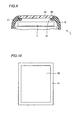
- Fig. 8 corresponds to Fig. 5, but a whole cross section of the mobile phone is shown in Fig. 8.
- a first modification of the second embodiment of the mobile phone according to the present invention will be described with reference to Fig. 8.
- mobile phone 1 basically has the same structure as mobile phone 1 shown in Figs. 5-7.
- concave portion 35 as shown in Fig. 5 is not formed on acrylic plate 32 constructing LCD window member 33.
- the cross section of acrylic plate 32 is generally rectangular. Similar to acrylic plate 32 shown in Figs. 5-7, acrylic plate 32 is a single layer of transparent material without any other film formed on the surface thereof. An opening, to which acrylic plate 32 as such can be fit, is formed in in-molded part 30.
- the form of acrylic plate 32 can be simplified so that the production cost of the mobile phone can further be decreased.
- mobile phone 1 includes a front case 6 and a rear case 36 constructing a casing.
- Members such as liquid crystal panel 7, a substrate 38 having a control circuit and the like mounted thereon, and a motor 37 for generating a vibration to notice an incoming call, are arranged inside the casing formed of front case 6 and rear case 36.
- Fig. 9 corresponds to Fig. 5.
- mobile phone 1 basically has the same structure as mobile phone 1 shown in Figs. 5-7.
- an opening 40 is formed in front case 6 as the casing.
- Acrylic plate 32 formed of a single layer of transparent material is arranged to cover opening 40.
- the region of acrylic plate 32 as the window member which is located above the emitting surface of liquid crystal panel 7 is the region to transmit light emitted from liquid crystal panel 7.
- Other film or the like is not formed on the surface of acrylic plate 32 in this region, just as acrylic plate 32 shown in Figs. 5-7.
- a silk screen print layer 41 as a colored layer having a prescribed color, character, pattern and the like formed thereon is formed on the back surface of acrylic plate 32.
- mobile phone 1 can further be simplified because in-molded part 30 as the frame member is unnecessary. This can decrease the production cost of mobile phone 1.
- an arbitrary design can be provided to acrylic plate 32 as the window member by forming silk screen print layer 41 of an arbitrary color and form on acrylic plate 32.
- the degree of freedom in designing mobile phone 1 can be ensured to some extent.
- the mobile phone is shown as the liquid crystal display device in the first and second embodiments of the present invention
- the present invention can be applied to various equipment using a liquid crystal panel, for example, equipment utilizing a liquid crystal panel in a display portion such as a personal digital assistant or a notebook computer, as well as a liquid crystal display device of a personal computer or a liquid crystal television.
- a liquid crystal display device is applicable not only to a mobile phone but also to the field of electronic equipment including a display portion for displaying text information, images and the like.
Landscapes
- Physics & Mathematics (AREA)
- Nonlinear Science (AREA)
- Mathematical Physics (AREA)
- Chemical & Material Sciences (AREA)
- Crystallography & Structural Chemistry (AREA)
- General Physics & Mathematics (AREA)
- Optics & Photonics (AREA)
- Devices For Indicating Variable Information By Combining Individual Elements (AREA)
- Liquid Crystal (AREA)
- Optical Elements Other Than Lenses (AREA)
- Telephone Set Structure (AREA)
Abstract
A liquid crystal display device and a liquid crystal panel which can
improve a display property are obtained. A liquid crystal display device
(1) includes an active matrix type liquid crystal panel (7) holding liquid
crystal, a window member (3) located on liquid crystal panel (7) and
transmitting light (26, 27a, 27b) emitted from liquid crystal panel (7), and
a diffusion member (19) located between liquid crystal (42) of liquid crystal
panel (7) and window member (3) and diffusing light (26) emitted from
liquid crystal (42).
Description
The present invention relates to a liquid crystal display device and a
liquid crystal panel and, more particularly, to a liquid crystal display
device and a liquid crystal panel that can prevent a degradation of display
quality.
In these days, mobile equipment such as a mobile phone is widely
used. Fig. 11 schematically shows a conventional mobile phone. Fig. 12
schematically shows a part of a cross section taken along the line XII-XII in
Fig. 11. Fig. 13 schematically shows a cross section of a liquid crystal
panel used in the mobile phone shown in Fig. 12. Fig. 14 is a schematic
cross-sectional view showing a mechanism of displaying an image or the
like on an LCD portion 102 of the mobile phone shown in Figs. 11-13.
A conventional mobile phone will be described with reference to Figs.
11-14.
Referring to Figs. 11-14, a conventional mobile phone 101 includes
an LCD (Liquid Crystal Display) portion 102, a receiver located on an
upper portion of a body of mobile phone 101, a microphone located on a
lower portion of the body, and an input portion for an input operation.
The receiver transmits to a user a voice of a person the user is speaking to.
The microphone is used for a voice input by a user. LCD portion 102 is for
a variable display of any kind of information, for example, text information
such as a list of telephone numbers or an e-mail, or video information such
as an image. In addition, an antenna is located on the upper portion of the
body.
A liquid crystal panel 107 is used in LCD portion 102, as shown in
Fig. 12. Liquid crystal panel 107 is held in a casing of mobile phone 101
formed of a front case 106 and a rear case (not shown). An opening is
formed in front case 106 in a region above an emitting surface of liquid
crystal panel 107 from which light is emitted. An in-molded part 103 is
arranged to cover the opening. In-molded part 103 is formed of a plastic
molded part 105 and an in-mold film 104 arranged on a surface of plastic
molded part 105. In-mold film 104 is a multilayer film and, as shown in
Fig. 14, includes a peel layer 123 located on a surface of plastic molded part
105 and an in-mold film top layer 122 located on peel layer 123. In-molded
part 103 is produced with a so-called in-mold method. This is a
method to produce an in-molded part which is an integrated product of
plastic molded part 105 and in-mold film 104 by one shot, through the step
of setting an in-mold film for the purpose of, for example, decoration or
function enhancement inside a mold used for plastic molding upon a plastic
molding process, and then performing a plastic molding process. Such in-molded
part 103 is adopted as means for enhancing a degree of freedom in
designing mobile phone 101 while preventing an increase in a production
cost.
An active matrix type liquid crystal panel has come to be used as
liquid crystal panel 107 to obtain high display quality. An exemplary
structure of such active matrix type liquid crystal panel 107 will be
described with reference to Fig. 13.
Referring to Fig. 13, liquid crystal panel 107 is a semipermeable type
color liquid crystal panel. In liquid crystal panel 107, a substrate 108 of a
transparent material such as glass having an element such as a thin film
field effect transistor, a switching element for controlling a display at each
pixel of a liquid crystal, formed on its surface and a CF (Color Filter)
substrate 109 having color filters 115a-115c arranged on a surface thereof,
are arranged opposite to each other to sandwich a liquid crystal 142
therebetween. Data lines 110a-110c which are conductive lines for
controlling the switching element, and transparent electrodes 111a-111c for
applying an electric field to liquid crystal 142 are arranged on a surface of
substrate 108 that faces liquid crystal 142. An orientation film 112a is
formed on surfaces of data lines 110a-110c and transparent electrodes
111a-111c that face liquid crystal 142.
A reflection film 116 for reflecting light incoming from an emitting
surface of liquid crystal panel 107 is formed on a surface of CF substrate
109 that faces liquid crystal 142. Color filters 115a-115c are arranged on
reflection film 116. Color filters 115a-115c are the filters of red, green and
blue colors, respectively. An overcoat film 114 is arranged on color filters
115a-115c. A transparent electrode 113 as an opposite electrode is
arranged on overcoat film 114. An orientation film 112b is arranged on
transparent electrode 113.
Liquid crystal 142 is held between orientation films 112a and 112b.
In addition, a seal material for holding liquid crystal 142 is arranged
between substrate 108 and CF substrate 109.
A phase difference plate (λ/4 plate) 117a is fixed on a surface of the
emitting surface side of the substrate in liquid crystal panel 107 with an
adhesion layer 119 interposed therebetween. A polarizer 118a is arranged
on phase difference plate 117a. In addition, a phase difference plate (λ/4
plate) 117b is fixed on that surface of CF substrate 109, which is opposite to
the surface facing liquid crystal 142, with an adhesion layer (not shown)
interposed therebetween. A polarizer 118b is arranged on that surface of
phase difference plate 117b which is opposite to the surface facing CF
substrate 109.
A mechanism of displaying an image on LCD portion 102 of mobile
phone 101 will be described with reference to Fig. 14.
Referring to Fig. 14, in LCD portion 102 of mobile phone 101, an
incident light 125 which enters liquid crystal panel 107 via in-molded part
103 comes into liquid crystal panel 107 from an emitting surface of liquid
crystal panel 107 (a surface facing to in-molded part 103). Incident light
125 is then reflected by reflection film 116 on a substrate portion 121 of
liquid crystal panel 107. The reflected light (reflected light 126) proceeds
from substrate portion 121 through adhesion layer 119, phase difference
plate 117a and polarizer 118a, and is emitted from the emitting surface of
liquid crystal panel 107. Reflected light 126 then exits the LCD portion of
mobile phone 101 via in-molded part 103. Reflected light 126 is colored by
color filters 115a-115c. Furthermore, an optical property of liquid crystal
142 can vary by altering a potential of each of transparent electrodes 111a-111c
by the switching element to modify an intensity, a direction or the like
of an electric field applied to liquid crystal 142. As a result, it is possible
to switch between the states transmitting and not transmitting reflected
light 126 of liquid crystal 142. Therefore, by controlling the switching
element corresponding to each pixel so as to display a prescribed character
or image, a prescribed character or image can be displayed on LCD portion
102.
The inventor found a following problem occurring in the LCD portion
of the conventional mobile phone as described above. That is, in
conventional mobile phone 101 described with reference to Figs. 11-14,
small light spots are sometimes seen all over the display surface in a liquid
crystal display of LCD portion 102, in addition to an image originally
displayed on the emitting surface of liquid crystal panel 107 (hereafter,
such small light spots generated will be called a glare.) Such glare is
especially seen when the environment is dark, for example, when mobile
phone 101 is used in the dark. Display quality of LCD portion 102 has
been lowered by a generation of this glare. In addition, as it is expected
that a user uses a mobile terminal such as mobile phone 101 under various
conditions, the use of a mobile phone in the dark environment as
mentioned above is supposed to be common. Therefore, the generation of
such glare is a serious problem which causes a degradation of the display
quality of LCD portion 102 of mobile phone 101.
The present invention aims to solve the problem as described above.
A purpose of the present invention is to provide a liquid crystal display
device and a liquid crystal panel which can improve the display property.
The inventor accomplished the present invention by studying and
finding a cause of the above-described glare generation. The inventor
thoroughly examined a structure of a mobile phone as a liquid crystal
display device generating a glare. As a result, a very small inequality
formed on peel layer 123 of in-mold film 104 constructing in-molded part
103 of mobile phone 101 was found as shown in Fig. 14. A pitch P1 of this
inequality was approximately 0.2 mm to 0.4 mm. It is probable that this
inequality of peel layer 123 was formed by a transfer of an inequality shape
formed on a surface of a drum around which in-mold film 104 was coiled
during a photogravure of in-mold film 104 prior to perform the in-mold
method.
Meanwhile, a pitch of the pixels of liquid crystal panel 107 is now
approximately 0.2 mm to 0.3 mm to attain a high resolution of liquid
crystal panel 107. In addition, reflected light 126 from liquid crystal panel
107 has an intensity distribution with a pitch corresponding to the pitch of
the pixels. Therefore, the pitch of the intensity distribution of reflected
light 126 will be nearly the same size as the pitch P1 of the inequality of
peel layer 123. As a result, the glare is generated by an interference of the
inequality of peel layer 123 of in-mold film 104 with reflected light 126
(that is, the glare is regarded as an unevenness of an interference of
reflected light 126 with the inequality of peel layer 123.)
Based on the findings of the inventor, a liquid crystal display device
in accordance with one aspect of the present invention includes an active
matrix type liquid crystal panel holding liquid crystal, a window member
located on the liquid crystal panel and transmitting light emitted from the
liquid crystal panel, and a diffusion member located between the liquid
crystal of the liquid crystal panel and the window member and diffusing
light emitted from the liquid crystal.
The light emitted from the liquid crystal panel has an intensity
distribution corresponding to the pixel pitch of the liquid crystal panel. In
addition, by diffusing the light emitted from the liquid crystal of the liquid
crystal panel to some degree by the diffusion member, a leveling of the
intensity distribution corresponding to the pixel pitch of the liquid crystal
panel is possible for the light emitted from the liquid crystal panel. With
this, if an inequality with a pitch similar to the pixel pitch is formed in a
light transmitting portion of the window member (if, for example, an
inequality with a pitch similar to the pixel pitch is formed on an in-mold
film constructing an in-molded part when the in-molded part or the like is
used as the window member), an interference of the light emitted from the
liquid crystal panel with the inequality formed on the window member as
mentioned above can be suppressed. Therefore, as the generation of the
so-called glare can be prevented, degradation of display quality of the liquid
crystal display device can be prevented.
The generation of the glare can also be prevented by using an in-molded
part or the like for the window member as mentioned above.
Therefore, the degree of freedom in designing a liquid crystal display device
can be enhanced while keeping high display quality of the liquid crystal
display device by applying the in-molded part or the like to the window
member.
In the liquid crystal display device in the aspect mentioned above, it
is preferred that the diffusion member includes a base material which can
transmit light, and a light diffusion material which is arranged dispersed
in the base material.
By this approach, a light diffusion property of the diffusion member
can be changed arbitrarily by modifying a size of the light diffusion
material dispersed in the base material and a distribution density of the
light diffusion material in the base material. With this, in the liquid
crystal display device, an optical property of the diffusion member can be
set to diffuse the light emitted from the liquid crystal panel so as to
decrease the glare without significantly degrading the high display quality
of the active matrix type liquid crystal panel.
In the liquid crystal display device in the aspect mentioned above, it
is preferred that the liquid crystal panel includes first and second
substrates holding the liquid crystal. The first substrate may be located
on the emitting surface side of the liquid crystal panel that emits light,
while the second substrate may be located in a region at a larger distance
from the emitting surface than the first substrate when seen from the
liquid crystal. Furthermore, the liquid crystal panel may include an
optical member arranged on that surface of the first substrate which is
opposite to the surface facing the liquid crystal. The diffusion member
may be located between the first substrate and the optical member.
By this approach, the diffusion member can be integrated in the
liquid crystal panel. With this, in a liquid crystal display device formed of
members such as a liquid crystal panel and a casing integrating the liquid
crystal panel, it is unnecessary to significantly modify the design of the
members other than the liquid crystal panel, such as the casing.
Therefore, by using the liquid crystal panel having the diffusion member,
the design of the members, such as the casing, of the conventional liquid
crystal display device can easily be applied to the liquid crystal display
device of the present invention. Consequently, a designing time period for
the members such as the casing to realize the liquid crystal display device
of the present invention can be shortened, so that the production cost of the
liquid crystal display device of the present invention is not increased.
In the liquid crystal display device in the aspect mentioned above, it
is preferred that the diffusion member is an adhesion layer that adheres
the optical member to the first substrate.
The adhesion layer that adheres the optical member to the first
substrate also exists in the conventional liquid crystal panel. Thus, the
shape of the liquid crystal panel similar to that of the conventional one can
be attained by adding a function of a diffusion member to the existing
adhesion layer. As a result, except for the liquid crystal panel of the liquid
crystal display device, almost the same members as the conventional ones
can be used. Therefore, the designing cost to realize the liquid crystal
display device of the present invention can further be decreased.
In the liquid crystal display device in the aspect mentioned above, a
preferred haze value of the diffusion member is between 50 % and 60 %.
In this example, if the haze value of the diffusion member is in the
range mentioned above, the generation of the glare can be prevented in the
liquid crystal display device by appropriately diffusing the light emitted
from the liquid crystal panel while maintaining the high display quality of
the active matrix type liquid crystal panel. It is to be noted that, a haze
value of the diffusion member is represented as a ratio of diffuse
transmitted light to total transmitted light when visible light is emitted to
the diffusion member: a haze value = (diffuse transmittance)/(total light
beam transmittance) x 100 (%).
A liquid crystal panel in accordance with another aspect of the
present invention is an active matrix type liquid crystal panel holding
liquid crystal, and includes first and second substrates holding liquid
crystal. The first substrate is located on an emitting surface side of the
liquid crystal panel that emits light, while the second substrate is located
in a region at a larger distance from the emitting surface than the first
substrate when seen from the liquid crystal. Furthermore, the liquid
crystal panel includes an optical member arranged on that surface of the
first substrate which is opposite to the surface facing the liquid crystal, and
a diffusion member located between the first substrate and the optical
member.
As described above, the light emitted from the liquid crystal panel
has an intensity distribution corresponding to the pixel pitch of the liquid
crystal panel. In addition, by diffusing the light emitted from the liquid
crystal of the liquid crystal panel (emitted light) to some degree by the
diffusion member, a leveling of the intensity distribution corresponding to
the pixel pitch of the liquid crystal panel is possible for the light emitted
from the liquid crystal panel. Assuming that a window member or the like
is arranged on the emitting surface of the liquid crystal panel. If an
inequality with a pitch similar to the pixel pitch is formed in a portion of
the window member which transmits light emitted from the liquid crystal
panel (if, for example, an inequality with a pitch similar to the pixel pitch is
formed on an in-mold film constructing an in-molded part when the in-molded
part or the like is used as the window member), an interference of
the light emitted from the liquid crystal panel with the inequality formed
on the window member can be suppressed because the intensity
distribution of the emitted light is leveled. Therefore, as the generation of
the so-called glare can be prevented, degradation of display quality of the
liquid crystal panel can be prevented.
In the liquid crystal panel in the another aspect mentioned above, it
is preferred that the diffusion member includes a base material which can
transmit light, and a light diffusion material which is arranged dispersed
in the base material.
By this approach, a light diffusion property of the diffusion member
can be changed arbitrarily by modifying a size of the light diffusion
material dispersed in the base material and a distribution density of the
light diffusion material in the base material. With this, an optical
property of the diffusion member can be set to diffuse the light emitted
from the liquid crystal panel so as to decrease the glare without
significantly degrading the high display quality of the active matrix type
liquid crystal panel.
In the liquid crystal panel in the another aspect mentioned above, it
is preferred that the diffusion member is an adhesion layer that adheres
the optical member to the first substrate.
As mentioned above, the adhesion layer that adheres the optical
member to the first substrate also exists in the conventional liquid crystal
panel. Thus, the shape of the liquid crystal panel similar to that of the
conventional one can be attained by adding a function of a diffusion
member to the existing adhesion layer. As a result, in the liquid crystal
display device having an integrated liquid crystal panel, almost the same
members as the conventional ones can be used except for the liquid crystal
panel. Therefore, the designing cost to realize the liquid crystal display
device using the liquid crystal panel according to the present invention can
further be decreased.
In the liquid crystal panel in the another aspect mentioned above, a
preferred haze value of the diffusion member is between 50 % and 60 %.
In this example, if the haze value of the diffusion member is in the
range mentioned above, an interference of the light emitted from the liquid
crystal panel with the inequality formed on the window member can be
prevented by appropriately diffusing the light emitted from the liquid
crystal panel while maintaining the high display quality of the active
matrix type liquid crystal panel, even if the window member having an
inequality with a pitch similar to the pixel pitch of the liquid crystal panel
formed thereon (such as the window member formed of an in-molded part
having an in-mold film including an inequality) is arranged on the emitting
surface of the liquid crystal panel.
A liquid crystal display device in accordance with another aspect of
the present invention includes an active matrix type liquid crystal panel, a
frame member located on the liquid crystal panel and having an opening
formed in a region located above an emitting surface of the liquid crystal
panel which emits light, and a window member located to cover the opening
of the frame member and transmitting light emitted from the emitting
surface of the liquid crystal panel. In the window member, the region that
transmits light emitted from the emitting surface of the liquid crystal panel
is formed of a single layer of transparent material.
As described above, the light emitted from the emitting surface of the
liquid crystal panel has an intensity distribution corresponding to the pixel
pitch of the liquid crystal panel. In addition, in the liquid crystal display
device in the above-mentioned aspect of the present invention, as the region
transmitting light emitted from the emitting surface of the liquid crystal
panel is formed of a single layer of transparent material, the region does
not have a multilayer structure as an in-molded part in which an in-mold
film is arranged on a surface of a plastic molded part. Therefore, there is
no phenomenon such as an interference of the inequality formed on the in-mold
film with the light emitted from the emitting surface of the liquid
crystal panel. This surely prevents the generation of the so-called glare.
Thus, degradation of a display property of the liquid crystal display device
by the glare can surely be prevented.
In addition, as the frame member is included besides the window
member, the degree of freedom in designing the liquid crystal display
device can be enhanced by arbitrarily changing the design of the frame
member while keeping the good display property.
A liquid crystal display device in accordance with another aspect of
the present invention includes an active matrix type liquid crystal panel, a
casing arranged to surround the liquid crystal panel and having an opening
formed in a region facing an emitting surface of the liquid crystal panel
which emits light, and a window member located to cover the opening of the
casing and transmitting light emitted from the emitting surface of the
liquid crystal panel. In the window member, the region that transmits
light emitted from a display surface of the liquid crystal panel is formed of
a single layer of transparent material.
As described above, the light emitted from the emitting surface of the
liquid crystal panel has an intensity distribution corresponding to the pixel
pitch of the liquid crystal panel. In addition, in the liquid crystal display
device in the above-mentioned aspect of the present invention, as the region
transmitting light emitted from the emitting surface of the liquid crystal
panel is formed of a single layer of transparent material, the region does
not have a multilayer structure as an in-molded part in which an in-mold
film is arranged on a surface of a plastic molded part. Therefore, there is
no phenomenon such as an interference of the inequality formed on the in-mold
film with the light emitted from the emitting surface of the liquid
crystal panel. This surely prevents the generation of the so-called glare.
Thus, degradation of a display property of the liquid crystal display device
by the glare can be prevented.
In the liquid crystal display device in the aspect mentioned above,
the window member may include a colored layer formed on a surface of a
region other than the region that transmits light emitted from the display
surface of the liquid crystal panel.
By this approach, an arbitrary design can be provided to the window
member by forming the colored layer of an arbitrary color and form on the
window member.
Embodiments of the present invention will now be described with
reference to the drawings. It is to be noted that, the same reference
character indicates the same or the corresponding portion and the
description thereof will not be repeated.
A first embodiment of a mobile phone according to the present
invention will be described with reference to Figs. 1-4.
Referring to Figs. 1-4, a mobile phone 1 includes an LCD (Liquid
Crystal Display) portion 2, a receiver located on an upper portion of a body
of mobile phone 1, a microphone located on a lower portion of the body, and
an input portion for an input operation. The receiver transmits to a user a
voice of a person the user is speaking to. The microphone is used for a
voice input by a user. LCD portion 2 is for a variable display of any kind
of information, for example, text information such as a list of telephone
numbers or an e-mail, or video information such as an image. In addition,
an antenna is located on the upper portion of the body.
A liquid crystal panel 7 is used in LCD portion 2, as shown in Fig. 2.
Liquid crystal panel 7 is held in a casing of mobile phone 1 formed of a
front case 6 and a rear case (not shown). An opening is formed in front
case 6 in a region above an emitting surface of liquid crystal panel 7 from
which light is emitted. An in-molded part 3 is arranged to cover the
opening. In-molded part 3 is formed of a plastic molded part 5 and an in-mold
film 4 arranged on a surface of plastic molded part 5. In-mold film 4
is a multilayer film and, as shown in Fig. 4, includes a peel layer 23 located
on a surface of plastic molded part 5 and an in-mold film top layer 22
located on peel layer 23. In-mold film top layer 22 includes an adhesion
layer and a layer which is colored or has a graphic for a design painted
thereon. In-molded part 3 is produced with a so-called in-mold method.
An active matrix type liquid crystal panel is applied as liquid crystal
panel 7 to obtain high display quality. A structure of the active matrix
type liquid crystal panel 7 applied to the mobile phone of the present
invention will be described with reference to Fig. 3.
Referring to Fig. 3, liquid crystal panel 7 is a semipermeable type
color liquid crystal panel. In liquid crystal panel 7, a substrate 8 as a first
substrate of a transparent material such as glass having an element such
as a thin film field effect transistor, a switching element for controlling a
display at each pixel of a liquid crystal, formed on its surface and a CF
substrate 9 as a second substrate having color filters 15a-15c arranged on a
surface thereof, are arranged opposite to each other to sandwich a liquid
crystal 42 therebetween. A switching element, data lines 10a-10c which
are conductive lines for controlling the switching element, and transparent
electrodes 11a-11c for applying an electric field to liquid crystal 42 are
arranged on a surface of substrate 8 that faces liquid crystal 42. An
orientation film 12a is formed on surfaces of data lines 10a-10c and
transparent electrodes 11a-11c that face liquid crystal 42.
A reflection film 16 for reflecting light incoming from the emitting
surface of liquid crystal panel 7 is formed on a surface of CF substrate 9
that faces liquid crystal 42. Color filters 15a-15c are arranged on
reflection film 16. Color filters 15a-15c are the filters of red, green and
blue colors, respectively. An overcoat film 14 is arranged on color filters
15a-15c. A transparent electrode 13 as an opposite electrode is arranged
on overcoat film 14. An orientation film 12b is arranged on transparent
electrode 13.
Liquid crystal 42 is held between orientation films 12a and 12b. In
addition, a seal material 24 for holding liquid crystal 42 is arranged
between substrate 8 and CF substrate 9.
A phase difference plate (λ/4 plate) 17a is fixed on a surface of the
emitting surface side of the substrate 8 in liquid crystal panel 7 with an
adhesion layer 19 as a diffusion member interposed therebetween. In
adhesion layer 19, a filler 20 as a light diffusion material is arranged
dispersed in an adhesive as a base material. Any member that can diffuse
light may be used as filler 20. Herein, the light diffusion material in a
powder or a particle form is arranged as filler 20 dispersed in the adhesive.
A polarizer 18a is arranged on phase difference plate 17a. In
addition, a phase difference plate (λ/4 plate) 17b is fixed on that surface of
CF substrate 9, which is opposite to the surface facing liquid crystal 42,
with an adhesion layer (not shown) interposed therebetween. A polarizer
18b is arranged on that surface of phase difference plate 17b which is
opposite to the surface facing CF substrate 109.
A mechanism of displaying an image and the like on LCD portion 2
of mobile phone 1 will be described with reference to Fig. 4.
Referring to Fig. 4, in LCD portion 2 (see Fig. 1) of mobile phone 1
(see Fig. 1), an incident light 25 which enters liquid crystal panel 7 via in-molded
part 3 comes into liquid crystal panel 7 from the emitting surface of
liquid crystal panel 7 (the surface facing in-molded part 3). Incident light
25 is then reflected by reflection film 16 (see Fig. 3) on a substrate portion
21 of liquid crystal panel 7. The reflected light 26 proceeds from substrate
portion 21 through adhesion layer 19, phase difference plate 17a and
polarizer 18a, and is emitted from the emitting surface of liquid crystal
panel 7. Reflected light 26 then exits the LCD portion 2 of mobile phone 1
via in-molded part 3. Reflected light 26 is colored by color filters 15a-15c.
Furthermore, an optical property of liquid crystal 42 can vary by altering a
potential of each of transparent electrodes 11a-11c by the switching
element to modify an intensity, a direction or the like of an electric field
applied to liquid crystal 42. As a result, it is possible to switch between
the states transmitting and not transmitting reflected light 26 of liquid
crystal 42. Therefore, by controlling the switching element corresponding
to each pixel so as to display a prescribed character or image, a prescribed
character or image can be displayed on LCD portion 2.
As described above, reflected light 26 emitted from liquid crystal
panel 7 has an intensity distribution corresponding to the pixel pitch of
liquid crystal panel 7. In addition, the existence of adhesion layer 19
including filler 20 enables reflected light 26 to be diffused to some degree
by adhesion layer 19 as a diffusion member. That is, as shown in Fig. 4, a
part of reflected light 26 can be diffused by filler 20 included in adhesion
layer 19 to be diffused light 27a and 27b. With this, a leveling of the
intensity distribution corresponding to the pixel pitch of liquid crystal
panel 7 is possible for reflected light 26. Thus, in the portion of in-molded
part 3 as the window member which transmits reflected light 26, if an
inequality with a pitch P1 similar to the pixel pitch is formed on peel layer
23 of in-mold film 4 constructing in-molded part 3, an interference of
reflected light 26 with the inequality of peel layer 23 as mentioned above
can be suppressed. Therefore, as the generation of the so-called glare can
be prevented, degradation of display quality of LCD portion 2 of mobile
phone 1 can be prevented.
In addition, as shown in Figs. 1-4, the generation of glare can be
suppressed even when in-molded part 3 having a high degree of freedom in
designing is used as the window member. Therefore, the degree of
freedom in designing mobile phone 1 can be enhanced while keeping high
display quality of LCD portion 2 in mobile phone 1 by using in-molded part
3 as the window member.
In addition, a light diffusion property of adhesion layer 19 can be
changed arbitrarily by modifying a size of filler 20 as the light diffusion
material dispersed in the adhesive as the base material, and a distribution
density of filler 20 in the adhesive. With this, in LCD portion 2 of mobile
phone 1, an optical property (a light diffusion property) of adhesion layer
19 can be set to diffuse reflected light 26 emitted from liquid crystal panel 7
so as to decrease the glare without degrading the high display quality of
active matrix type liquid crystal panel 7.
It is to be noted that, in liquid crystal panel 7, the distribution
density of filler 20 is adjusted such that a haze value of adhesion layer 19
as the diffusion member becomes 52 %. Herein, a preferred haze value of
adhesion layer 19 is between 50 % and 60 %.
In this example, if the haze value of adhesion layer 19 is in the range
mentioned above, the generation of the glare can surely be prevented by
appropriately diffusing reflected light 26 emitted from liquid crystal panel
7 while maintaining the high display quality of the active matrix type
liquid crystal panel 7 in LCD portion 2 of mobile phone 1.
In addition, adhesion layer 19 as the diffusion member is interposed
between substrate 8 as the first substrate and phase difference plate 17a as
the optical member, and has a function to fix phase difference plate 17a on
substrate 8. Thus, adhesion layer 19 as the diffusion member is a member
constructing liquid crystal panel 7. Therefore, except for liquid crystal
panel 7, it is unnecessary to significantly modify the design of the members,
such as the casing, of mobile phone 1 integrating liquid crystal panel 7.
Using liquid crystal panel 7 according to the present invention as shown in
Fig. 3, the design of the members, such as the casing, of the conventional
mobile phone can easily be applied to the mobile phone 1 of the present
invention. Consequently, a designing time period for the members such as
the casing of mobile phone 1 can be shortened according to the present
invention, so that the production cost of mobile phone 1 of the present
invention is not increased.
In addition, adhesion layer 19 also exists in the conventional liquid
crystal panel shown in Fig. 13. Thus, the shape of the liquid crystal panel
7 similar to that of the conventional one can be attained by adding a
function of a diffusion member to the existing adhesion layer 19 by adding
filler 20 thereto. As a result, except for liquid crystal panel 7 of mobile
phone 1, almost the same members as the conventional ones can be used.
Therefore, the designing cost of mobile phone 1 according to the present
invention can further be decreased.
A second embodiment of the mobile phone according to the present
invention will be described with reference to Figs. 5-7. Fig. 5 corresponds
to Fig. 2.
Referring to Figs. 5-7, the mobile phone basically has the same
structure as the mobile phone in the first embodiment of the present
invention. In the mobile phone in the first embodiment of the present
invention, however, in-molded part 3 is arranged as the window member on
the emitting surface of liquid crystal panel 7. In mobile phone 1 shown in
Figs. 5-7, an LCD window member 33 formed of an acrylic plate 32 as a
window member and a frame-shaped in-molded part 30 as a frame member
is arranged on the emitting surface of liquid crystal panel 7. An opening
31 is formed in in-molded part 30. In-molded part 30 is formed of a frame-shaped
plastic molded part 29 and an in-mold film 28 arranged on a surface
of plastic molded part 29. Acrylic plate 32 is secured fitted to opening 31
of in-molded part 30. A convex portion 34 for securing acrylic plate 32 is
formed on opening 31 of in-molded part 30. A concave portion 35
corresponding to this step portion 34 is also formed on acrylic plate 32.
Acrylic plate 32 is secured to in-molded part 30 by press-fixing concave
portion 35 of acrylic plate 32 to convex portion 34 of in-molded part 30.
Acrylic plate 32 is a single layer of transparent material without any other
film formed on the surface thereof. A liquid crystal panel having a
structure similar to that of the conventional liquid crystal panel shown in
Fig. 13 is used as liquid crystal panel 7.
As described above, light emitted from the emitting surface of liquid
crystal panel 7 (i.e., reflected light 26 (see Fig. 4)) has an intensity
distribution corresponding to the pixel pitch of liquid crystal panel 7. In
addition, in mobile phone 1 as a liquid crystal display device shown in Figs.
5 and 6, the region in acrylic plate 32 as the window member that
transmits light emitted from the emitting surface of liquid crystal panel 7 is
formed of a single layer of transparent material. That means, this region
in acrylic plate 32 does not have a multilayer structure as in-molded part
30 in which in-mold film 28 is arranged on a surface of plastic molded part
29. Because of the absence of the in-mold film including the inequality on
the surface of acrylic plate 32, there is no phenomenon such as an
interference of the light emitted from the emitting surface of liquid crystal
panel 7 with such inequality. This surely prevents the generation of the
so-called glare.
Furthermore, as in-molded part 30 as the frame member is included
besides acrylic plate 32 as the window member, the degree of freedom in
designing mobile phone 1 can be enhanced by arbitrarily changing the
design of in-molded part 30 while keeping the good display property of LCD
portion 2.
Fig. 8 corresponds to Fig. 5, but a whole cross section of the mobile
phone is shown in Fig. 8. A first modification of the second embodiment of
the mobile phone according to the present invention will be described with
reference to Fig. 8.
Referring to Fig. 8, mobile phone 1 basically has the same structure
as mobile phone 1 shown in Figs. 5-7. In mobile phone 1 shown in Fig. 8,
however, concave portion 35 as shown in Fig. 5 is not formed on acrylic
plate 32 constructing LCD window member 33. In mobile phone 1 shown
in Fig. 8, the cross section of acrylic plate 32 is generally rectangular.
Similar to acrylic plate 32 shown in Figs. 5-7, acrylic plate 32 is a single
layer of transparent material without any other film formed on the surface
thereof. An opening, to which acrylic plate 32 as such can be fit, is formed
in in-molded part 30.
With such a structure, in addition to the similar effect as the mobile
phone shown in Figs. 5-7 being obtained, the form of acrylic plate 32 can be
simplified so that the production cost of the mobile phone can further be
decreased.
It is to be noted that, as shown in Fig. 8, mobile phone 1 includes a
front case 6 and a rear case 36 constructing a casing. Members such as
liquid crystal panel 7, a substrate 38 having a control circuit and the like
mounted thereon, and a motor 37 for generating a vibration to notice an
incoming call, are arranged inside the casing formed of front case 6 and
rear case 36.
A second modification of the second embodiment of the mobile phone
according to the present invention will be described with reference to Figs.
9 and 10. Fig. 9 corresponds to Fig. 5.
Referring to Figs. 9 and 10, mobile phone 1 basically has the same
structure as mobile phone 1 shown in Figs. 5-7. In the region located
above the emitting surface of liquid crystal panel 7, however, an opening 40
is formed in front case 6 as the casing. Acrylic plate 32 formed of a single
layer of transparent material is arranged to cover opening 40. The region
of acrylic plate 32 as the window member which is located above the
emitting surface of liquid crystal panel 7 is the region to transmit light
emitted from liquid crystal panel 7. Other film or the like is not formed on
the surface of acrylic plate 32 in this region, just as acrylic plate 32 shown
in Figs. 5-7.
On the outer circumference of acrylic plate 32, a silk screen print
layer 41 as a colored layer having a prescribed color, character, pattern and
the like formed thereon is formed on the back surface of acrylic plate 32.
In this example, because of the absence of the in-mold film including
the inequality on the surface of acrylic plate 32 as the mobile phone shown
in Figs. 5-7, there is no phenomenon such as an interference of the light
emitted from the emitting surface of liquid crystal panel 7 with such
inequality. This surely prevents the generation of the so-called glare.
In addition, comparing with mobile phone 1 shown in Figs. 5-7, the
structure of mobile phone 1 can further be simplified because in-molded
part 30 as the frame member is unnecessary. This can decrease the
production cost of mobile phone 1.
Furthermore, an arbitrary design can be provided to acrylic plate 32
as the window member by forming silk screen print layer 41 of an arbitrary
color and form on acrylic plate 32. As a result, the degree of freedom in
designing mobile phone 1 can be ensured to some extent.
It should be noted that, though the mobile phone is shown as the
liquid crystal display device in the first and second embodiments of the
present invention, the present invention can be applied to various
equipment using a liquid crystal panel, for example, equipment utilizing a
liquid crystal panel in a display portion such as a personal digital assistant
or a notebook computer, as well as a liquid crystal display device of a
personal computer or a liquid crystal television.
Though the embodiments of the present invention have been
described above, features of each embodiment may be combined
appropriately. In addition, the embodiments disclosed herein are by way
of illustration in all points and should not be taken by way of limitation.
The scope of the present invention is indicated not by the above-mentioned
embodiments but by the appended claims, and it is intended to encompass
all modifications falling within the equivalent spirit and scope of the
appended claims.
A liquid crystal display device according to the present invention is
applicable not only to a mobile phone but also to the field of electronic
equipment including a display portion for displaying text information,
images and the like.
Claims (12)
- A liquid crystal display device, comprising:an active matrix type liquid crystal panel (7) holding liquid crystal (42);a window member (3) located on said liquid crystal panel (7) and transmitting light (26, 27a, 27b) emitted from said liquid crystal panel (7); anda diffusion member (19) located between liquid crystal (42) of said liquid crystal panel (7) and said window member (3) and diffusing light (26) emitted from said liquid crystal (42).
- The liquid crystal display device according to claim 1, wherein said diffusion member (19) includesa base material capable of transmitting light, anda light diffusion material (20) arranged dispersed in said base material.
- The liquid crystal display device according to claim 1, wherein said liquid crystal panel (7) includesfirst and second substrates (8, 9) holding said liquid crystal, said first substrate (8) being located on an emitting surface side of said liquid crystal panel (7) that emits light, while said second substrate (9) being located in a region at a larger distance from said emitting surface than said first substrate (8) when seen from said liquid crystal (42), andan optical member (17a) arranged on that surface of said first substrate (8) which is opposite to the surface facing said liquid crystal (42); andsaid diffusion member (19) is located between said first substrate (8) and said optical member (17a).
- The liquid crystal display device according to claim 3, wherein said diffusion member (19) is an adhesion layer adhering said optical member (17a) to said first substrate (8).
- The liquid crystal display device according to claim 1, wherein a haze value of said diffusion member (19) is between 50 % and 60 %.
- An active matrix type liquid crystal panel (7) holding liquid crystal (42), comprising:first and second substrates (8, 9) holding said liquid crystal (42), said first substrate (8) being located on an emitting surface side of said liquid crystal panel (7) that emits light, while said second substrate (9) being located in a region at a larger distance from said emitting surface than said first substrate (8) when seen from said liquid crystal (42);an optical member (17a) arranged on that surface of said first substrate (8) which is opposite to the surface facing said liquid crystal (42); anda diffusion member (19) located between said first substrate (8) and said optical member (17a).
- The liquid crystal panel according to claim 6, wherein
said diffusion member (19) includes
a base material capable of transmitting light, and
a light diffusion material (20) arranged dispersed in said base material. - The liquid crystal panel according to claim 6, wherein
said diffusion member (19) is an adhesion layer adhering said optical member (17a) to said first substrate (8). - The liquid crystal panel according to claim 6, wherein
a haze value of said diffusion member (19) is between 50 % and 60 %. - A liquid crystal display device, comprising:an active matrix type liquid crystal panel (7);a frame member (30) located on said liquid crystal panel (7) and having an opening (31) formed in a region located above an emitting surface of said liquid crystal panel (7) that emits light; anda window member (32) located to cover opening (31) of said frame member (30) and transmitting light emitted from the emitting surface of said liquid crystal panel (7); whereinsaid window member (32) has a region that transmits light emitted from the emitting surface of said liquid crystal panel, said region being formed of a single layer of transparent material.
- A liquid crystal display device, comprising:an active matrix type liquid crystal panel (7);a casing (6) arranged to surround said liquid crystal panel (7) and having an opening (40) formed in a region facing an emitting surface of said liquid crystal panel that emits light; anda window member (32) located to cover opening (40) of said casing (6) and transmitting light emitted from the emitting surface of said liquid crystal panel (7); wherein
said window member (32) has a region that transmits light emitted from the emitting surface of said liquid crystal panel, said region being formed of a single layer of transparent material. - The liquid crystal display device according to claim 11, wherein said window member (32) includes a colored layer (41) formed on a surface of a region other than the region that transmits light emitted from the emitting surface of said liquid crystal panel (7).
Applications Claiming Priority (1)
| Application Number | Priority Date | Filing Date | Title |
|---|---|---|---|
| PCT/JP2001/000201 WO2002056102A1 (en) | 2001-01-15 | 2001-01-15 | Lcd device and lcd panel |
Publications (2)
| Publication Number | Publication Date |
|---|---|
| EP1353216A1 true EP1353216A1 (en) | 2003-10-15 |
| EP1353216A4 EP1353216A4 (en) | 2005-02-16 |
Family
ID=11736913
Family Applications (1)
| Application Number | Title | Priority Date | Filing Date |
|---|---|---|---|
| EP01900766A Withdrawn EP1353216A4 (en) | 2001-01-15 | 2001-01-15 | LIQUID CRYSTAL DISPLAY DEVICE AND PANEL |
Country Status (5)
| Country | Link |
|---|---|
| US (1) | US20030020682A1 (en) |
| EP (1) | EP1353216A4 (en) |
| JP (1) | JP3808035B2 (en) |
| CN (1) | CN1416536A (en) |
| WO (1) | WO2002056102A1 (en) |
Cited By (1)
| Publication number | Priority date | Publication date | Assignee | Title |
|---|---|---|---|---|
| JP2003107440A (en) * | 2001-09-28 | 2003-04-09 | Asahi Glass Co Ltd | Transflective liquid crystal display element |
Families Citing this family (3)
| Publication number | Priority date | Publication date | Assignee | Title |
|---|---|---|---|---|
| US7373180B2 (en) * | 2001-05-25 | 2008-05-13 | Kyocera Wireless Corp. | Method and apparatus for accentuating graphical elements on a mobile handset housing |
| US7763063B2 (en) * | 2003-09-03 | 2010-07-27 | Bolton Medical, Inc. | Self-aligning stent graft delivery system, kit, and method |
| JP4015090B2 (en) * | 2003-09-08 | 2007-11-28 | 株式会社東芝 | Stereoscopic display device and image display method |
Family Cites Families (10)
| Publication number | Priority date | Publication date | Assignee | Title |
|---|---|---|---|---|
| JP3219943B2 (en) * | 1994-09-16 | 2001-10-15 | 株式会社東芝 | Planar direct-view display device |
| JPH09325204A (en) * | 1996-05-31 | 1997-12-16 | Sony Corp | Optical filter, image display device and liquid crystal display device using the same |
| JP3552084B2 (en) * | 1997-05-29 | 2004-08-11 | 日東電工株式会社 | Circularly polarized light separating plate, manufacturing method thereof, optical element, polarized light source device and liquid crystal display device |
| JP4101339B2 (en) * | 1997-09-25 | 2008-06-18 | 大日本印刷株式会社 | Light diffusing film, manufacturing method thereof, polarizing plate with diffusing layer, and liquid crystal display device |
| JP4010047B2 (en) * | 1998-02-18 | 2007-11-21 | ソニー株式会社 | Reflective display device |
| JPH11237624A (en) * | 1998-02-20 | 1999-08-31 | Seiko Epson Corp | Liquid crystal devices and electronic equipment |
| JPH11289169A (en) * | 1998-04-03 | 1999-10-19 | Nec Shizuoka Ltd | Information display window for electronic device |
| JP3995797B2 (en) * | 1998-05-12 | 2007-10-24 | 凸版印刷株式会社 | Coating liquid for light scattering film |
| JP2000075132A (en) * | 1998-08-27 | 2000-03-14 | Nitto Denko Corp | Scattering elliptically polarizing plate and liquid crystal display |
| WO2000019267A1 (en) * | 1998-09-29 | 2000-04-06 | Matsushita Electric Industrial Co., Ltd. | Reflection liquid crystal display |
-
2001
- 2001-01-15 US US10/204,279 patent/US20030020682A1/en not_active Abandoned
- 2001-01-15 EP EP01900766A patent/EP1353216A4/en not_active Withdrawn
- 2001-01-15 CN CN01806355.1A patent/CN1416536A/en active Pending
- 2001-01-15 JP JP2002556297A patent/JP3808035B2/en not_active Expired - Fee Related
- 2001-01-15 WO PCT/JP2001/000201 patent/WO2002056102A1/en not_active Ceased
Cited By (1)
| Publication number | Priority date | Publication date | Assignee | Title |
|---|---|---|---|---|
| JP2003107440A (en) * | 2001-09-28 | 2003-04-09 | Asahi Glass Co Ltd | Transflective liquid crystal display element |
Also Published As
| Publication number | Publication date |
|---|---|
| WO2002056102A1 (en) | 2002-07-18 |
| JP3808035B2 (en) | 2006-08-09 |
| EP1353216A4 (en) | 2005-02-16 |
| US20030020682A1 (en) | 2003-01-30 |
| CN1416536A (en) | 2003-05-07 |
| JPWO2002056102A1 (en) | 2004-05-20 |
Similar Documents
| Publication | Publication Date | Title |
|---|---|---|
| US20060193148A1 (en) | Light-emitting diode backlight assembly and liquid crystal display device using the same | |
| CN109459880A (en) | Display module and display device | |
| CN112002223A (en) | Display cover plate, preparation method thereof and display device | |
| GB2423622A (en) | Light-emitting-diode backlight assembly and liquid crystal display device using the same | |
| CN108089386B (en) | Covers, Display Modules and Mobile Terminals | |
| CN101950041A (en) | Display filter and containment vessel with GTG | |
| CN108566453A (en) | Cover plate, display module and mobile terminal | |
| KR100495499B1 (en) | Liquid crystal display device, portable terminal and display equipment provided with the liquid crystal display device | |
| CN108089362A (en) | Display module, manufacturing method of display module and mobile terminal | |
| US20040105265A1 (en) | Color layer material, color filter substrate, electro-optic device and electronic device, fabrication method of color filter substrate, and manufacturing method of electro-optic device | |
| CN113687543B (en) | Display module and display device | |
| EP1353216A1 (en) | Lcd device and lcd panel | |
| US7088407B2 (en) | Color filter substrate, method of manufacturing color filter substrate, electro-optical device, method of manufacturing electro-optical device, and electronic apparatus | |
| CN115685617A (en) | display device | |
| US20090273736A1 (en) | Liquid Display Device and Method for Fabricating the Same | |
| TW546519B (en) | Passive matrix liquid crystal display | |
| JP4106238B2 (en) | Transflective dual-use display device substrate, transflective liquid crystal display device, and electronic equipment | |
| US7804562B2 (en) | Liquid crystal panel with a uniform background color | |
| US7580094B2 (en) | Transreflective LCD panel and electronic device using the same | |
| CN115274801B (en) | Display panel, preparation method thereof and display device | |
| JP2003248444A (en) | Electro-optical device substrate, electro-optical device and electronic equipment | |
| JP4133171B2 (en) | Transflective LCD panel | |
| JP4622821B2 (en) | Display of portable information processing device | |
| JP2003084282A (en) | Liquid crystal display | |
| JP2005182009A (en) | Display device and image display method |
Legal Events
| Date | Code | Title | Description |
|---|---|---|---|
| PUAI | Public reference made under article 153(3) epc to a published international application that has entered the european phase |
Free format text: ORIGINAL CODE: 0009012 |
|
| 17P | Request for examination filed |
Effective date: 20020822 |
|
| AK | Designated contracting states |
Kind code of ref document: A1 Designated state(s): AT BE CH CY DE DK ES FI FR GB GR IE IT LI LU MC NL PT SE TR |
|
| RBV | Designated contracting states (corrected) |
Designated state(s): AT BE CH DE FR GB LI |
|
| STAA | Information on the status of an ep patent application or granted ep patent |
Free format text: STATUS: THE APPLICATION HAS BEEN WITHDRAWN |
|
| A4 | Supplementary search report drawn up and despatched |
Effective date: 20050105 |
|
| 18W | Application withdrawn |
Effective date: 20050117 |