EP1351490A1 - Image sensor with improved readout circuit - Google Patents
Image sensor with improved readout circuit Download PDFInfo
- Publication number
- EP1351490A1 EP1351490A1 EP02252385A EP02252385A EP1351490A1 EP 1351490 A1 EP1351490 A1 EP 1351490A1 EP 02252385 A EP02252385 A EP 02252385A EP 02252385 A EP02252385 A EP 02252385A EP 1351490 A1 EP1351490 A1 EP 1351490A1
- Authority
- EP
- European Patent Office
- Prior art keywords
- pixel
- reset
- read
- image sensor
- signal
- Prior art date
- Legal status (The legal status is an assumption and is not a legal conclusion. Google has not performed a legal analysis and makes no representation as to the accuracy of the status listed.)
- Granted
Links
- 238000000034 method Methods 0.000 claims description 9
- 238000006243 chemical reaction Methods 0.000 description 9
- 239000003990 capacitor Substances 0.000 description 7
- 230000006870 function Effects 0.000 description 5
- 238000005070 sampling Methods 0.000 description 5
- 238000002347 injection Methods 0.000 description 3
- 239000007924 injection Substances 0.000 description 3
- 239000002184 metal Substances 0.000 description 3
- 230000008901 benefit Effects 0.000 description 2
- 230000000875 corresponding effect Effects 0.000 description 2
- 101000963523 Homo sapiens Magnesium transporter MRS2 homolog, mitochondrial Proteins 0.000 description 1
- 101000589392 Homo sapiens Pannexin-1 Proteins 0.000 description 1
- 102100039143 Magnesium transporter MRS2 homolog, mitochondrial Human genes 0.000 description 1
- 102100032361 Pannexin-1 Human genes 0.000 description 1
- 101100545229 Saccharomyces cerevisiae (strain ATCC 204508 / S288c) ZDS2 gene Proteins 0.000 description 1
- 101100113084 Schizosaccharomyces pombe (strain 972 / ATCC 24843) mcs2 gene Proteins 0.000 description 1
- 101100167209 Ustilago maydis (strain 521 / FGSC 9021) CHS8 gene Proteins 0.000 description 1
- 230000008859 change Effects 0.000 description 1
- 230000002596 correlated effect Effects 0.000 description 1
- 230000003247 decreasing effect Effects 0.000 description 1
- 230000003111 delayed effect Effects 0.000 description 1
- 238000010586 diagram Methods 0.000 description 1
- 230000004048 modification Effects 0.000 description 1
- 238000012986 modification Methods 0.000 description 1
- 230000008569 process Effects 0.000 description 1
- 230000009467 reduction Effects 0.000 description 1
- 239000007787 solid Substances 0.000 description 1
- 230000009897 systematic effect Effects 0.000 description 1
- 230000001052 transient effect Effects 0.000 description 1
Images


Classifications
-
- H—ELECTRICITY
- H04—ELECTRIC COMMUNICATION TECHNIQUE
- H04N—PICTORIAL COMMUNICATION, e.g. TELEVISION
- H04N25/00—Circuitry of solid-state image sensors [SSIS]; Control thereof
- H04N25/60—Noise processing, e.g. detecting, correcting, reducing or removing noise
- H04N25/65—Noise processing, e.g. detecting, correcting, reducing or removing noise applied to reset noise, e.g. KTC noise related to CMOS structures by techniques other than CDS
-
- H—ELECTRICITY
- H04—ELECTRIC COMMUNICATION TECHNIQUE
- H04N—PICTORIAL COMMUNICATION, e.g. TELEVISION
- H04N25/00—Circuitry of solid-state image sensors [SSIS]; Control thereof
- H04N25/50—Control of the SSIS exposure
- H04N25/57—Control of the dynamic range
-
- H—ELECTRICITY
- H04—ELECTRIC COMMUNICATION TECHNIQUE
- H04N—PICTORIAL COMMUNICATION, e.g. TELEVISION
- H04N25/00—Circuitry of solid-state image sensors [SSIS]; Control thereof
- H04N25/60—Noise processing, e.g. detecting, correcting, reducing or removing noise
- H04N25/67—Noise processing, e.g. detecting, correcting, reducing or removing noise applied to fixed-pattern noise, e.g. non-uniformity of response
-
- H—ELECTRICITY
- H04—ELECTRIC COMMUNICATION TECHNIQUE
- H04N—PICTORIAL COMMUNICATION, e.g. TELEVISION
- H04N25/00—Circuitry of solid-state image sensors [SSIS]; Control thereof
- H04N25/70—SSIS architectures; Circuits associated therewith
- H04N25/71—Charge-coupled device [CCD] sensors; Charge-transfer registers specially adapted for CCD sensors
- H04N25/75—Circuitry for providing, modifying or processing image signals from the pixel array
-
- H—ELECTRICITY
- H04—ELECTRIC COMMUNICATION TECHNIQUE
- H04N—PICTORIAL COMMUNICATION, e.g. TELEVISION
- H04N25/00—Circuitry of solid-state image sensors [SSIS]; Control thereof
- H04N25/70—SSIS architectures; Circuits associated therewith
- H04N25/76—Addressed sensors, e.g. MOS or CMOS sensors
-
- H—ELECTRICITY
- H04—ELECTRIC COMMUNICATION TECHNIQUE
- H04N—PICTORIAL COMMUNICATION, e.g. TELEVISION
- H04N25/00—Circuitry of solid-state image sensors [SSIS]; Control thereof
- H04N25/70—SSIS architectures; Circuits associated therewith
- H04N25/76—Addressed sensors, e.g. MOS or CMOS sensors
- H04N25/77—Pixel circuitry, e.g. memories, A/D converters, pixel amplifiers, shared circuits or shared components
Definitions
- This invention relates to solid state active pixel image sensors suitable for implementation in CMOS technology.
- the invention may be applied to an image sensor of the type having active pixels each comprising a photodiode and three transistors.
- image sensors use the technique known as Correlated Double Sampling (CDS) in which two sampling steps are used whereby a reset voltage and a signal voltage for each pixel are stored on capacitors in the column, and the difference between these voltages is processed by the readout chain.
- CDS improves fixed pattern noise in the final image, but although the subtraction process removes low frequency pixel noise it increases high frequency noise.
- the requirement for two readout steps limits the maximum operating frequency of the camera, and the provision of the storage capacitors increases the column area and contributes kT/C sampling noise.
- the present invention provides an image sensor as defined in claim 1. From another aspect, the invention provides a method of operating an image sensor as defined in claim 8.
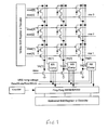
- FIG. 1 shows, by way of example, a 3x3 active pixel array.
- Each pixel 10 includes a photodiode 12 and a transistor pair MN2, MR1 which forms the upper half of a NMOS source follower structure.
- Each column contains a column line 16 and a second column line 20. To minimise the capacitance of these two lines, they are best routed in layers of metal with the Vx metal (line 16) above the VRT metal (line 20).
- the two column lines 16 and 20 are connected to a Read-Reset Amplifier (RR Amp) circuit 22.
- Figure 2 shows the schematic of the RR Amp circuit 22.
- One such circuit is contained at the base of each column and serves a column of pixels 10, one of which is seen in Figure 2.
- the RR Amp circuit 22 is essentially a single stage amplifier which uses transistors MR1 and MN2 in the pixel as one half of a differential pair, and the column current source MCS1 and MCS2 as the long tail pair bias current.
- Transistors MP1 and MP2 form a current source load which can be configured by means of transistors MPS1 and MPS2.
- MR1, MRS1 are used to read and reset the pixel, respectively.
- MR2 is present to match MR1 but the gate is always held at VDDHI.
- MRS2 is used in reset mode to configure the amplifier as a unity gain buffer.
- Figure 2 shows the RRAmp 22 configured as a comparator.
- the output stage is only used when the circuit is configured as a comparator and provides rail-to-rail logic.
- ResetMode 1
- ReadMode 0
- ReadModeBar 1
- the bandwidth of the pixel is much larger than that of the RRAmp 22 and so this noise reduction will be small; the situation can be improved by boosting the bias current to the RRAmp during reset and increasing the reset switch resistance.
- the reset pulse fall-time can be increased to allow the amplifier more time to correct for charge injection.
- the output gain can be increased by making transistor M1 larger than the pixel source follower transistor Mn2. This introduces a systematic offset into the amplifier but this is cancelled by the operation of the RRAmp 22.
- the achievable gain from this circuit is typically around 45dB in a 0.35 ⁇ m CMOS technology.
- the circuit as thus far described cancels fixed pattern noise (FPN) arising from both pixel-to-pixel offset variations due to Vt mismatches of pixel transistors and also column offsets due to mismatches of column amplifiers.
- FPN fixed pattern noise
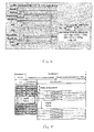
- Figure 4 illustrates the timing applied to the circuit of Figures 1 and 2 to achieve this, in one embodiment.
- Figure 5 shows the same timing in terms of line information. It will be seen that the number of lines of offset between resetting a given row of pixels and reading out their signal data determines the exposure period, and by adjusting the number of lines of offset the exposure of the image can be adjusted.
- the store 26 is used to provide this offset, and must be capable of storing an entire frame if the maximum offset is to be available.
- RRAmps 22 reduces the spread of voltages which must be converted in a reset frame and thus reduces the framestore memory requirements. Moreover when configured as an open loop high-gain amplifier or comparator, the RRAmp has a very low input referred noise which reduces the remaining readout noise level.
- Figure 6 shows a modification in which the Read-Reset amplifier is used to provide a two step AD converter.
- a two-step ADC can reduce power consumption and increase the output conversion rate of a column-parallel single slope AD converter.
- a ramp generator 30 provides a coarse ramp waveform which comprises a series of steps, and a fine ramp waveform which is a single slope.
- the coarse ramp voltage drives the inputs of the array of column comparators and also a local capacitor Cx.
- the output of the comparator 22 changes from a 1 to a 0, causing ramp switch 32 to close and store the current ramp voltage locally in the column.
- the fine ramp voltage is applied to the bottom plate of the column capacitors Cx.
- the column capacitors Cx can be efficiently implemented in NMOS as N-well structures, where the N-well forms the bottom plate and is shared between columns by virtue of always being at a common potential.
- the node Vbot is at approximately a coarse LSB voltage above ground to create a positive system offset for fine ramping.
- the fine ramp voltage drives Vbot.
- the fine ramp voltage starts from ground and sweeps over the LSB range of the coarse conversion. Some overrange can be built in to take account of charge injection introduced by the Vtop sampling switch and avoid ramp transient non-linearity.
- the deltaV on the Vtop node at the beginning of fine conversion will be around a coarse LSB voltage below the pixel output voltage, by virtue of switching Vbot from a coarse LSB voltage to ground. This will reset all comparators into an output high state.
- the Cx capacitor size must be chosen for some desired kT/C noise level and charge injection offset.
- the sampling switch should be minimum geometry.
- the coarse ramp must have a much higher drive strength then the fine ramp, since it is driving a set of parallel grounded capacitors Cx with a greater slew rate. However, since the coarse ramp is used for only a brief part of the overall conversion cycle, the coarse ramp can be shut down when it is not in use.
- the coarse ramp generator must settle to fine LSB level within a clock cycle.
- the SRAM bank 26 is divided into fine and coarse sub-banks 26a and 26b. These banks receive a fine and a coarse count which is latched by the change of state of the comparator switch 32 during fine and coarse conversion phases.
- the present invention thus provides an improved means of reducing fixed pattern noise and kT/C noise.
- the invention enables a "double read" method to be implemented with a reduced size of frame store, potentially allowing SRAM rather than DRAM storage to be used.
Landscapes
- Engineering & Computer Science (AREA)
- Multimedia (AREA)
- Signal Processing (AREA)
- Transforming Light Signals Into Electric Signals (AREA)
Abstract
Description
If the voltage Vref exceeds Vpix the output node Vc=AVDD, otherwise Vc=0V.
The column capacitors Cx can be efficiently implemented in NMOS as N-well structures, where the N-well forms the bottom plate and is shared between columns by virtue of always being at a common potential. During the coarse conversion phase, the node Vbot is at approximately a coarse LSB voltage above ground to create a positive system offset for fine ramping. During fine conversion the fine ramp voltage drives Vbot. The fine ramp voltage starts from ground and sweeps over the LSB range of the coarse conversion. Some overrange can be built in to take account of charge injection introduced by the Vtop sampling switch and avoid ramp transient non-linearity.
Claims (9)
- An image sensor comprising:an array of pixels arranged in rows and columns; each pixel having a light-sensitive element and switching means operable to apply a reset signal to the pixel and to read out a signal voltage from the pixel;each column comprising a read-reset circuit which is operable in a first mode to read pixel reset voltages and in a second mode to read pixel signals;analogue-to-digital converter means for converting the pixel reset voltages and the pixel signals to digital form; anda memory arranged to store the digital representations of the reset voltages of the pixels for up to a complete frame.
- An image sensor according to claim 1, in which the analogue-to-digital converter means comprises each read-reset circuit in said second mode operating as a comparator and including a ramp generator whereby an output is set when the ramp voltage equals the signal voltage, the analogue-to-digital converter means further comprising a counter providing a count which is latched by said set output.
- An image sensor according to claim 2, in which the ramp generator is a single slope generator.
- An image sensor according to claim 2, in which the ramp generator comprises a coarse ramp generator which provides a step-wise ramp and a fine ramp generator which provides a single-slope ramp.
- An image sensor according to any preceding claim, further including subtraction means arranged to subtract, from the pixel signal of a given pixel, the reset signal of the same pixel retrieved from the memory.
- An image sensor according to claim 5, in which the memory is controllable to offset readout of the pixel signal and readout of the reset signal by a given number of line periods, whereby to set the exposure of the sensor.
- An image sensor according to any preceding claim, in which the memory is a DRAM or SRAM.
- A method of operating an image sensor, which image sensor comprises an array of pixels arranged in rows and columns, each pixel having a light-sensitive element and switching means operable to apply a reset signal to the pixel and to read out reset and signal voltages from the pixel, each column comprising a read-reset circuit which is operable in a first mode to read pixel reset voltages and in a second mode to read pixel signals; the method comprising the steps of:operating each read-reset circuit in said first mode to read said pixel rows of reset voltages;converting the read pixel reset voltages to digital form and storing these in a memory;operating said read-reset circuits in said second mode to read rows of said pixel signals and converting these to digital form;operation in said first and second modes being interleaved by rows; andsubtracting from the digital representations of the pixel signals of each row the corresponding digital pixel reset voltage representations retrieved from said memory.
- The method of claim 8, in which the readout of the reset and pixel signal values for each line are separated in time by an offset which can be controllably adjusted to set the exposure of the sensor.
Priority Applications (3)
| Application Number | Priority Date | Filing Date | Title |
|---|---|---|---|
| EP02252385A EP1351490B1 (en) | 2002-04-02 | 2002-04-02 | Image sensor with improved readout circuit |
| DE60234810T DE60234810D1 (en) | 2002-04-02 | 2002-04-02 | Image sensor with improved readout circuit |
| US10/405,904 US7911512B2 (en) | 2002-04-02 | 2003-04-02 | Image sensor with readout circuit |
Applications Claiming Priority (1)
| Application Number | Priority Date | Filing Date | Title |
|---|---|---|---|
| EP02252385A EP1351490B1 (en) | 2002-04-02 | 2002-04-02 | Image sensor with improved readout circuit |
Publications (2)
| Publication Number | Publication Date |
|---|---|
| EP1351490A1 true EP1351490A1 (en) | 2003-10-08 |
| EP1351490B1 EP1351490B1 (en) | 2009-12-23 |
Family
ID=27838147
Family Applications (1)
| Application Number | Title | Priority Date | Filing Date |
|---|---|---|---|
| EP02252385A Expired - Lifetime EP1351490B1 (en) | 2002-04-02 | 2002-04-02 | Image sensor with improved readout circuit |
Country Status (3)
| Country | Link |
|---|---|
| US (1) | US7911512B2 (en) |
| EP (1) | EP1351490B1 (en) |
| DE (1) | DE60234810D1 (en) |
Cited By (4)
| Publication number | Priority date | Publication date | Assignee | Title |
|---|---|---|---|---|
| FR2866180A1 (en) * | 2004-02-06 | 2005-08-12 | St Microelectronics Sa | METHOD OF PROCESSING INFORMATION DELIVERED BY AN ACTIVE PIXEL MATRIX OF A SENSOR PROVIDING EXTENDED DYNAMIC AND GAIN, AND CORRESPONDING SENSOR. |
| GB2421376A (en) * | 2004-12-15 | 2006-06-21 | Micron Technology Inc | Analogue to digital converter utilising multimode ramp generator |
| WO2008146236A1 (en) | 2007-05-25 | 2008-12-04 | Uti Limited Partnership | Circuit providing low-noise readout |
| CN106027923A (en) * | 2015-03-30 | 2016-10-12 | 佳能株式会社 | Photoelectric conversion apparatus and photoelectric conversion system |
Families Citing this family (19)
| Publication number | Priority date | Publication date | Assignee | Title |
|---|---|---|---|---|
| JP4247995B2 (en) * | 2005-02-03 | 2009-04-02 | 富士通マイクロエレクトロニクス株式会社 | Data readout circuit for solid-state image sensor, imaging apparatus, and data readout method for solid-state image sensor |
| US8013920B2 (en) * | 2006-12-01 | 2011-09-06 | Youliza, Gehts B.V. Limited Liability Company | Imaging system for creating an image of an object |
| US8289430B2 (en) * | 2007-02-09 | 2012-10-16 | Gentex Corporation | High dynamic range imaging device |
| US8587706B2 (en) | 2008-01-30 | 2013-11-19 | Gentex Corporation | Imaging device |
| JP5319161B2 (en) * | 2008-05-21 | 2013-10-16 | パナソニック株式会社 | Solid-state imaging device |
| KR101512737B1 (en) * | 2008-11-06 | 2015-04-22 | 삼성전자주식회사 | Pixel sensor array and image sensor using the same |
| EP2362640B1 (en) * | 2010-02-15 | 2019-05-01 | CSEM Centre Suisse d'Electronique et de Microtechnique SA - Recherche et Développement | Compact low noise signal readout circuit and method for operating thereof |
| JP5704939B2 (en) * | 2011-01-31 | 2015-04-22 | オリンパス株式会社 | Imaging device |
| US9041838B2 (en) | 2012-02-14 | 2015-05-26 | Gentex Corporation | High dynamic range imager system |
| KR101293057B1 (en) * | 2012-03-13 | 2013-08-05 | 동국대학교 산학협력단 | Comparator, analog digital converter, ramp signal slope calibration circuit, cmos image sensor using the same and ramp signal slope calibration method |
| US9177987B2 (en) | 2012-10-12 | 2015-11-03 | Samsung Electronics Co., Ltd. | Binary CMOS image sensors, methods of operating same, and image processing systems including same |
| JP5870954B2 (en) * | 2013-03-29 | 2016-03-01 | ソニー株式会社 | Comparator, solid-state imaging device, electronic device, and driving method |
| FR3012912B1 (en) * | 2013-11-04 | 2017-04-14 | E2V Semiconductors | SILICON-BASED IMAGE SENSOR WITH ENHANCED READING DYNAMIC |
| CN105519096B (en) | 2014-07-14 | 2021-02-19 | 索尼公司 | Comparator, AD converter, solid-state imaging device, electronic apparatus, and comparator control method |
| KR20160008877A (en) * | 2014-07-15 | 2016-01-25 | 삼성전자주식회사 | An image sensor |
| KR101653622B1 (en) * | 2015-05-07 | 2016-09-05 | 고려대학교 산학협력단 | Image sensor for extracting edge information |
| US9848140B2 (en) * | 2016-03-31 | 2017-12-19 | Omnivision Technologies, Inc. | Horizontal banding reduction with ramp generator isolation in an image sensor |
| KR102772735B1 (en) | 2019-04-08 | 2025-02-27 | 삼성전자주식회사 | Image sensor device and operation method thereof |
| CN116132826A (en) * | 2023-02-20 | 2023-05-16 | 中国电子科技集团公司第四十四研究所 | Image sensor capable of adaptively adjusting tail current |
Citations (2)
| Publication number | Priority date | Publication date | Assignee | Title |
|---|---|---|---|---|
| EP0617552A2 (en) | 1993-03-24 | 1994-09-28 | Sony Corporation | Solid-state imaging device |
| WO1999044359A1 (en) | 1998-02-27 | 1999-09-02 | Intel Corporation | Method to reduce reset noise in photodiode based cmos image sensors |
Family Cites Families (4)
| Publication number | Priority date | Publication date | Assignee | Title |
|---|---|---|---|---|
| US5153421A (en) * | 1991-11-04 | 1992-10-06 | Xerox Corporation | Architecture for analog and digital image sensor arrays |
| US6809766B1 (en) * | 1998-03-11 | 2004-10-26 | Micro Technology, Inc. | Look ahead rolling shutter system in CMOS sensors |
| US6362767B1 (en) * | 1999-03-22 | 2002-03-26 | The Board Of Trustees Of The Leland Stanford Junior University | Methods for simultaneous analog-to-digital conversion and multiplication |
| US6965407B2 (en) * | 2001-03-26 | 2005-11-15 | Silicon Video, Inc. | Image sensor ADC and CDS per column |
-
2002
- 2002-04-02 EP EP02252385A patent/EP1351490B1/en not_active Expired - Lifetime
- 2002-04-02 DE DE60234810T patent/DE60234810D1/en not_active Expired - Lifetime
-
2003
- 2003-04-02 US US10/405,904 patent/US7911512B2/en not_active Expired - Lifetime
Patent Citations (2)
| Publication number | Priority date | Publication date | Assignee | Title |
|---|---|---|---|---|
| EP0617552A2 (en) | 1993-03-24 | 1994-09-28 | Sony Corporation | Solid-state imaging device |
| WO1999044359A1 (en) | 1998-02-27 | 1999-09-02 | Intel Corporation | Method to reduce reset noise in photodiode based cmos image sensors |
Cited By (17)
| Publication number | Priority date | Publication date | Assignee | Title |
|---|---|---|---|---|
| FR2866180A1 (en) * | 2004-02-06 | 2005-08-12 | St Microelectronics Sa | METHOD OF PROCESSING INFORMATION DELIVERED BY AN ACTIVE PIXEL MATRIX OF A SENSOR PROVIDING EXTENDED DYNAMIC AND GAIN, AND CORRESPONDING SENSOR. |
| US7667753B2 (en) | 2004-02-06 | 2010-02-23 | Stmicroelectronics S.A. | Method for processing information delivered by a sensor pixel matrix offering a wide dynamic range and gain and corresponding sensor |
| GB2421374B (en) * | 2004-12-15 | 2007-01-10 | Micron Technology Inc | Ramp generators for imager analog-to-digital converters |
| USRE41767E1 (en) | 2004-12-15 | 2010-09-28 | Aptina Imaging Corporation | Ramp generators for imager analog-to-digital converters |
| GB2421374A (en) * | 2004-12-15 | 2006-06-21 | Micron Technology Inc | Ramp generators for imager analogue-to-digital converters |
| GB2421376B (en) * | 2004-12-15 | 2007-01-10 | Micron Technology Inc | Ramp generators for imager analog-to-digital converters |
| US7274319B2 (en) | 2004-12-15 | 2007-09-25 | Micron Technology, Inc. | Ramp generators for imager analog-to-digital converters |
| US7075470B2 (en) | 2004-12-15 | 2006-07-11 | Micron Technology, Inc. | Ramp generators for imager analog-to-digital converters |
| GB2421376A (en) * | 2004-12-15 | 2006-06-21 | Micron Technology Inc | Analogue to digital converter utilising multimode ramp generator |
| WO2008146236A1 (en) | 2007-05-25 | 2008-12-04 | Uti Limited Partnership | Circuit providing low-noise readout |
| US9609243B2 (en) | 2007-05-25 | 2017-03-28 | Uti Limited Partnership | Systems and methods for providing low-noise readout of an optical sensor |
| CN106027923A (en) * | 2015-03-30 | 2016-10-12 | 佳能株式会社 | Photoelectric conversion apparatus and photoelectric conversion system |
| EP3076663A3 (en) * | 2015-03-30 | 2016-12-28 | Canon Kabushiki Kaisha | Photoelectric conversion apparatus and photoelectric conversion system |
| US9813649B2 (en) | 2015-03-30 | 2017-11-07 | Canon Kabushiki Kaisha | Photoelectric conversion apparatus and photoelectric conversion system |
| RU2638914C2 (en) * | 2015-03-30 | 2017-12-18 | Кэнон Кабусики Кайся | Photoelectric conversion device and photoelectric conversion system |
| US10142573B2 (en) | 2015-03-30 | 2018-11-27 | Canon Kabushiki Kaisha | Photoelectric conversion apparatus and photoelectric conversion system |
| CN106027923B (en) * | 2015-03-30 | 2019-07-12 | 佳能株式会社 | Photoelectric conversion device and photo-translating system |
Also Published As
| Publication number | Publication date |
|---|---|
| US7911512B2 (en) | 2011-03-22 |
| DE60234810D1 (en) | 2010-02-04 |
| EP1351490B1 (en) | 2009-12-23 |
| US20030193595A1 (en) | 2003-10-16 |
Similar Documents
| Publication | Publication Date | Title |
|---|---|---|
| EP1351490B1 (en) | Image sensor with improved readout circuit | |
| US8687097B2 (en) | Solid-state image-pickup device, method for driving solid-state image-pickup device, and image-pickup apparatus | |
| US6885331B2 (en) | Ramp generation with capacitors | |
| KR101450904B1 (en) | A/d conversion circuit, control method thereof, solid-state imaging device, and imaging apparatus | |
| JP5880478B2 (en) | Comparator, solid-state imaging device, electronic device, and driving method | |
| USRE41865E1 (en) | CMOS image sensor having a chopper-type comparator to perform analog correlated double sampling | |
| US7375672B2 (en) | Analog-to-digital conversion method, analog-to-digital converter, semiconductor device for detecting distribution of physical quantity, and electronic apparatus | |
| JP5870954B2 (en) | Comparator, solid-state imaging device, electronic device, and driving method | |
| US10250826B2 (en) | Image sensors having extended dynamic range | |
| JP5636694B2 (en) | Electronic device, AD converter, AD conversion method | |
| US7586523B2 (en) | Amplification-type CMOS image sensor of wide dynamic range | |
| US7741988B2 (en) | Analog-digital converter, solid-state image capturing apparatus, and electronic information device | |
| US6818933B2 (en) | CMOS image sensors | |
| US20030227040A1 (en) | Image sensor | |
| US8081243B2 (en) | Correlated double sampling circuit and CMOS image sensor unit | |
| JP2024530079A (en) | PIXEL ARRAY, IMAGE SENSOR, AND METHOD FOR OPERATING A PIXEL ARRAY - Patent application | |
| US8334492B2 (en) | Solid-state imaging device, Imaging device, and semiconductor device | |
| US20120006973A1 (en) | Image sensor with sample and hold circuitry for addressing time variant noise | |
| US7649488B1 (en) | Low-power column parallel cyclic analog-to-digital converter | |
| KR102506833B1 (en) | Ramp Signal Generator, and CMOS Image Sensor Using That | |
| US20040165088A1 (en) | Low light sensor signal to noise improvement | |
| JP2011029843A (en) | Solid-state imaging apparatus | |
| JP2015053708A (en) | Electronic device, AD converter, AD conversion method |
Legal Events
| Date | Code | Title | Description |
|---|---|---|---|
| PUAI | Public reference made under article 153(3) epc to a published international application that has entered the european phase |
Free format text: ORIGINAL CODE: 0009012 |
|
| AK | Designated contracting states |
Kind code of ref document: A1 Designated state(s): AT BE CH CY DE DK ES FI FR GB GR IE IT LI LU MC NL PT SE TR |
|
| AX | Request for extension of the european patent |
Extension state: AL LT LV MK RO SI |
|
| 17P | Request for examination filed |
Effective date: 20040322 |
|
| AKX | Designation fees paid |
Designated state(s): DE FR GB IT |
|
| 17Q | First examination report despatched |
Effective date: 20080519 |
|
| GRAP | Despatch of communication of intention to grant a patent |
Free format text: ORIGINAL CODE: EPIDOSNIGR1 |
|
| GRAS | Grant fee paid |
Free format text: ORIGINAL CODE: EPIDOSNIGR3 |
|
| GRAA | (expected) grant |
Free format text: ORIGINAL CODE: 0009210 |
|
| AK | Designated contracting states |
Kind code of ref document: B1 Designated state(s): DE FR GB IT |
|
| REG | Reference to a national code |
Ref country code: GB Ref legal event code: FG4D |
|
| REF | Corresponds to: |
Ref document number: 60234810 Country of ref document: DE Date of ref document: 20100204 Kind code of ref document: P |
|
| PLBE | No opposition filed within time limit |
Free format text: ORIGINAL CODE: 0009261 |
|
| STAA | Information on the status of an ep patent application or granted ep patent |
Free format text: STATUS: NO OPPOSITION FILED WITHIN TIME LIMIT |
|
| 26N | No opposition filed |
Effective date: 20100924 |
|
| PG25 | Lapsed in a contracting state [announced via postgrant information from national office to epo] |
Ref country code: IT Free format text: LAPSE BECAUSE OF FAILURE TO SUBMIT A TRANSLATION OF THE DESCRIPTION OR TO PAY THE FEE WITHIN THE PRESCRIBED TIME-LIMIT Effective date: 20091223 |
|
| PGFP | Annual fee paid to national office [announced via postgrant information from national office to epo] |
Ref country code: FR Payment date: 20120522 Year of fee payment: 11 |
|
| PGFP | Annual fee paid to national office [announced via postgrant information from national office to epo] |
Ref country code: GB Payment date: 20130326 Year of fee payment: 12 |
|
| PGFP | Annual fee paid to national office [announced via postgrant information from national office to epo] |
Ref country code: DE Payment date: 20130322 Year of fee payment: 12 |
|
| REG | Reference to a national code |
Ref country code: FR Ref legal event code: ST Effective date: 20131231 |
|
| PG25 | Lapsed in a contracting state [announced via postgrant information from national office to epo] |
Ref country code: FR Free format text: LAPSE BECAUSE OF NON-PAYMENT OF DUE FEES Effective date: 20130430 |
|
| REG | Reference to a national code |
Ref country code: DE Ref legal event code: R119 Ref document number: 60234810 Country of ref document: DE |
|
| GBPC | Gb: european patent ceased through non-payment of renewal fee |
Effective date: 20140402 |
|
| PG25 | Lapsed in a contracting state [announced via postgrant information from national office to epo] |
Ref country code: GB Free format text: LAPSE BECAUSE OF NON-PAYMENT OF DUE FEES Effective date: 20140402 Ref country code: DE Free format text: LAPSE BECAUSE OF NON-PAYMENT OF DUE FEES Effective date: 20141101 |
|
| REG | Reference to a national code |
Ref country code: DE Ref legal event code: R079 Ref document number: 60234810 Country of ref document: DE Free format text: PREVIOUS MAIN CLASS: H04N0003150000 Ipc: H04N0005378000 |