EP1351306A2 - Memory structures - Google Patents
Memory structures Download PDFInfo
- Publication number
- EP1351306A2 EP1351306A2 EP03252042A EP03252042A EP1351306A2 EP 1351306 A2 EP1351306 A2 EP 1351306A2 EP 03252042 A EP03252042 A EP 03252042A EP 03252042 A EP03252042 A EP 03252042A EP 1351306 A2 EP1351306 A2 EP 1351306A2
- Authority
- EP
- European Patent Office
- Prior art keywords
- electrode
- memory
- storage element
- memory storage
- conductive
- Prior art date
- Legal status (The legal status is an assumption and is not a legal conclusion. Google has not performed a legal analysis and makes no representation as to the accuracy of the status listed.)
- Withdrawn
Links
Images



Classifications
-
- H—ELECTRICITY
- H10—SEMICONDUCTOR DEVICES; ELECTRIC SOLID-STATE DEVICES NOT OTHERWISE PROVIDED FOR
- H10N—ELECTRIC SOLID-STATE DEVICES NOT OTHERWISE PROVIDED FOR
- H10N70/00—Solid-state devices having no potential barriers, and specially adapted for rectifying, amplifying, oscillating or switching
- H10N70/20—Multistable switching devices, e.g. memristors
- H10N70/231—Multistable switching devices, e.g. memristors based on solid-state phase change, e.g. between amorphous and crystalline phases, Ovshinsky effect
-
- G—PHYSICS
- G11—INFORMATION STORAGE
- G11C—STATIC STORES
- G11C17/00—Read-only memories programmable only once; Semi-permanent stores, e.g. manually-replaceable information cards
- G11C17/14—Read-only memories programmable only once; Semi-permanent stores, e.g. manually-replaceable information cards in which contents are determined by selectively establishing, breaking or modifying connecting links by permanently altering the state of coupling elements, e.g. PROM
- G11C17/18—Auxiliary circuits, e.g. for writing into memory
-
- H—ELECTRICITY
- H10—SEMICONDUCTOR DEVICES; ELECTRIC SOLID-STATE DEVICES NOT OTHERWISE PROVIDED FOR
- H10B—ELECTRONIC MEMORY DEVICES
- H10B61/00—Magnetic memory devices, e.g. magnetoresistive RAM [MRAM] devices
- H10B61/10—Magnetic memory devices, e.g. magnetoresistive RAM [MRAM] devices comprising components having two electrodes, e.g. diodes or MIM elements
-
- H—ELECTRICITY
- H10—SEMICONDUCTOR DEVICES; ELECTRIC SOLID-STATE DEVICES NOT OTHERWISE PROVIDED FOR
- H10B—ELECTRONIC MEMORY DEVICES
- H10B63/00—Resistance change memory devices, e.g. resistive RAM [ReRAM] devices
- H10B63/20—Resistance change memory devices, e.g. resistive RAM [ReRAM] devices comprising selection components having two electrodes, e.g. diodes
- H10B63/22—Resistance change memory devices, e.g. resistive RAM [ReRAM] devices comprising selection components having two electrodes, e.g. diodes of the metal-insulator-metal type
-
- H—ELECTRICITY
- H10—SEMICONDUCTOR DEVICES; ELECTRIC SOLID-STATE DEVICES NOT OTHERWISE PROVIDED FOR
- H10B—ELECTRONIC MEMORY DEVICES
- H10B63/00—Resistance change memory devices, e.g. resistive RAM [ReRAM] devices
- H10B63/80—Arrangements comprising multiple bistable or multi-stable switching components of the same type on a plane parallel to the substrate, e.g. cross-point arrays
- H10B63/84—Arrangements comprising multiple bistable or multi-stable switching components of the same type on a plane parallel to the substrate, e.g. cross-point arrays arranged in a direction perpendicular to the substrate, e.g. 3D cell arrays
-
- H—ELECTRICITY
- H10—SEMICONDUCTOR DEVICES; ELECTRIC SOLID-STATE DEVICES NOT OTHERWISE PROVIDED FOR
- H10B—ELECTRONIC MEMORY DEVICES
- H10B63/00—Resistance change memory devices, e.g. resistive RAM [ReRAM] devices
- H10B63/80—Arrangements comprising multiple bistable or multi-stable switching components of the same type on a plane parallel to the substrate, e.g. cross-point arrays
- H10B63/84—Arrangements comprising multiple bistable or multi-stable switching components of the same type on a plane parallel to the substrate, e.g. cross-point arrays arranged in a direction perpendicular to the substrate, e.g. 3D cell arrays
- H10B63/845—Arrangements comprising multiple bistable or multi-stable switching components of the same type on a plane parallel to the substrate, e.g. cross-point arrays arranged in a direction perpendicular to the substrate, e.g. 3D cell arrays the switching components being connected to a common vertical conductor
-
- H—ELECTRICITY
- H10—SEMICONDUCTOR DEVICES; ELECTRIC SOLID-STATE DEVICES NOT OTHERWISE PROVIDED FOR
- H10N—ELECTRIC SOLID-STATE DEVICES NOT OTHERWISE PROVIDED FOR
- H10N70/00—Solid-state devices having no potential barriers, and specially adapted for rectifying, amplifying, oscillating or switching
- H10N70/801—Constructional details of multistable switching devices
- H10N70/821—Device geometry
- H10N70/823—Device geometry adapted for essentially horizontal current flow, e.g. bridge type devices
Definitions
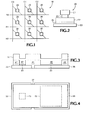
- FIG. 1 is a simplified schematic diagram of an embodiment of a cross-point memory array 10 in which the disclosed memory cell structures can be utilized.
- the memory arrangement 10 includes row selection conductor lines R0, R1, R2 and column selection conductor lines C0, C1, C2.
- a memory cell 20 is connected between each row selection conductor line R0, R1, R2 and each column selection conductor line C0, C1, C2.
- the row selection conductor lines and the column selection conductor lines are referred to by "row” and “column” terminology for convenience, and that in actual implementations the memory cells 20 do not necessarily have to be physically arranged in rows and columns.
- Each memory cell is basically uniquely accessed or selected by a first selection line and a second selection line that can be oriented in different ways.
- the column lines do not have to be orthogonal to the row lines, but are illustrated in that manner for ease of understanding.
- FIG. 2 is a simplified electrical block diagram of an embodiment of the memory cell 20 which includes a memory storage element 23 that is electrically connected to a control element 25 by an electrode E2.
- the memory storage element 23 and the control element 25 are serially connected between an electrode E1 and an electrode E3.
- the electrodes E1-E3 comprise conductive elements such as conductors, conductive regions or other conductive features, and it should be appreciated that the electrode E2 can comprise one or more electrically conductive elements.
- the memory storage element 23 is configured as a change state memory storage element, while the control element 25 is configured as a control element for the change state memory storage element and provides current to the memory storage element. More particularly, the memory storage element is configured to predictably and reliably break down at a lower energy level than the control element, while the control tunnel junction region is configured for sustained operation as a control element for the memory.
- Each of the memory storage element 23 and the control element 25 includes a cross-sectional area through which current flows.
- such area can be defined by the overlap of the interfaces between the element and the electrodes on either side of the element.
- the control element 25 and the memory element 23 can be of the same device type, and the control element 25 has a cross-sectional area that is greater than the cross-sectional area of the memory storage element, for example such that the memory storage element will break down at a lower energy level than the control element.
- the ratio between the control element cross-sectional area and the memory storage element cross-sectional area can be selected so that the memory storage element functions as a state change memory storage element, while the control element has control element cross-sectional area configured for sustained operation as a control element for the memory storage element.
- the memory storage element 23 changes state at a lower energy level than the control element 25, which allows the memory storage element to be programmed.
- a memory cell is programmed by selectively providing sufficient energy to the cell to cause the memory storage element to break down.
- a memory cell is read by providing a lesser amount of energy to cell and sensing whether current flows through the cell.
- the ratio between the cross-sectional area of the control element and the cross-sectional area of the memory storage element can be in the range of about 2 to 20.
- the memory storage element 23 can be an antifuse device, such as a programmable tunnel junction device.
- the antifuse device can be either a dielectric rupture type device or a tunnel junction device.
- the tunnel junction can be formed from oxidized metal, thermally grown oxide, or deposited oxides or nitrides.
- the memory storage element may also be embodied with semiconductor materials such as polysilicon, polycrystalline silicon, amorphous silicon, microcrystalline silicon, metal filament electro migration, trap induced hysterisis, ferroelectric capacitor, Hall effect, and polysilicon resistors.
- Other embodiments of the memory storage element include tunneling magneto-resistive or capacitive elements as floating gates.
- the memory storage element can be a read only LeComber or silicide switch or a re-writable phase-change material including a write-erase-write phase change material.
- the memory storage element can also comprise a PIN diode or a Schottky diode.
- the control element 25 can comprise a tunnel junction device or PN, PIN or Schottky diodes. Other diodes that can be used include Zener diodes, avalanche diodes, tunnel diodes, and a four layer diode such as a silicon controlled rectifier. Also, the control element 25 can be a junction field effect or bipolar transistor. The control element 25 is sized sufficiently to carry an adequate current such that the state of the storage element 23 can be changed. When the control element is a diode, it can be formed using doped polysilicon, amorphous silicon, or microcrystalline silicon.
- the memory storage element 23 and the control element can also be of the same device type, wherein both can comprise tunnel junction devices, Schottky diodes, or PIN diodes, for example.
- the disclosed memory structures are described as employing tunnel junction devices as the memory storage elements and control elements, and it should be appreciated that the memory storage elements and control elements can be implemented as described previously.
- the disclosed memory structures will be shown as integrated circuits that include interlayer dielectric such as silicon dioxide, silicon nitride, or TEOS (tetraethylorthosilicate) that provide support and isolation between various structures of an integrated circuit.
- interlayer dielectric such as silicon dioxide, silicon nitride, or TEOS (tetraethylorthosilicate) that provide support and isolation between various structures of an integrated circuit.
- the ILD can be deposited using several different technologies such as chemical vapor deposition (CVD), atmospheric pressure CVD, low pressure CVD, plasma enhanced CVD, physical vapor deposition (PVD), and sputtering.
- CVD chemical vapor deposition
- PVD physical vapor deposition
- sputtering regions and layers of such dielectric are identified in the drawings by the reference designation ILD.
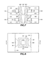
- FIGS. 3 and 4 schematically depict an embodiment of a memory cell that includes a memory storage element 23 disposed on a first conductor 33.
- a control element 25 is disposed on a second conductor 35 that is laterally or transversely adjacent the first conductor 33.
- the memory storage element 23 and the control element 25 are thus horizontally, transversely or laterally separated and each can have a generally horizontal planar extent.
- the first and second conductors 33, 35 can be substantially coplanar, and the memory storage element 23 and the control element 25 can also be substantially co-planar.
- a dielectric layer 41 is disposed over the first and second conductors 33, 35 and includes openings 47, 49 over the memory storage element 23 and the control element 25.
- a conductive layer 37 is disposed on the dielectric layer 41 and extends into the openings 47, 49 so as to form an electrode between the memory storage element 23 and the control element 25.
- the memory storage element 23 can be formed of an oxide of the first conductor 33, while the control element 25 can be formed of an oxide of the underlying second conductor 35.
- the memory storage element 23 can be formed of an oxide that is different from an oxide of the first conductor 33
- the control element 25 can be formed of an oxide that is different from an oxide of the second conductor 35.
- the memory storage element 23 can also be a portion of an unpatterned oxide layer that can be a deposited oxide layer or a completely oxidized deposited metal layer, for example.
- the control element 25 can be a portion of an unpatterned oxide layer that can be a deposited oxide layer or a completely oxidized deposited metal layer, for example.
- FIGS. 5 and 6 schematically depict an embodiment of a memory structure that includes a plurality of memory cells each including a memory storage element 23 disposed between the rim edge of a conductive well or tub 27 and a conductor 833 or 837 that is vertically adjacent the rim edge.
- Each memory cell further includes a control element 25 disposed between the base of the conductive tub 27 and a conductor 833 or 835 that is vertically adjacent the base.
- the memory storage element 23 and/or the control element 25 can have a horizontally planar extent, and are vertically separated.
- the memory cells of FIGS. 5 and 6 can be implemented in stacked layers for example wherein a conductor 833 that is vertically adjacent the rim edge of a given conductive tub 27 is vertically adjacent the base of a conductive tub 27 that is in an adjacent layer.
- the conductor 833 can be a row selection line while the conductors 835, 837 can be column selection lines in a cross-point memory structure.
- a conductive tub 27 can be laterally offset relative to the conductor 833 that is vertically adjacent the rim of such conductive tub 27, for example to control the area of the memory tunnel junction oxide region 23. As a result, a conductive tub 27 is laterally offset relative to another vertically adjacent conductive tub 27 in an adjacent layer.
- the memory storage element 23 can formed of an oxide of the conductive tub 27, and the control element 25 can be formed of an oxide of the conductor 833 or 835 that is vertically adjacent the base of the conductive tub 27.
- the memory tunnel junction oxide region 23 can be formed of an oxide that is different from an oxide of the rim of the conductive tub 27, and the control tunnel junction oxide region 25 can be formed of an oxide that is different from an oxide of the conductor 833 or 835.
- the memory storage element 23 can also be a portion of an unpatterned oxide layer that can be a deposited oxide layer or a completely oxidized deposited metal layer, for example.
- the control element 25 can be a portion of an unpatterned oxide layer that can be a deposited oxide layer or a completely oxidized deposited metal layer, for example.
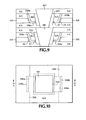
- FIGS. 7 and 8 schematically depict an embodiment of a memory structure that includes memory cells each including a memory storage element 23 disposed between a conductive well or tub 133 and a conductive region or block 139 that is laterally adjacent the conductive tub 133.
- a control element 25 is disposed between the conductive block 139 and a conductor 135 that is laterally adjacent the conductive block 139.
- the memory storage element 23 and the control element 25 of a memory cell of FIGS. 5 and 6 are thus horizontally separated and each can be planar with a vertical extent.
- the conductive block 139 can be a truncated wedge, and the memory storage element 23 and the control element 25 are in contact with opposing faces of the truncated wedge.
- a vertical conductive via or pillar 141 is disposed in the conductive well 133, and can extend through an aperture in the base of the conductive tub 133.
- the conductive pillar 141 and the conductive tub 133 form a conductive structure having a vertical extent.
- the conductive tub 133 can be omitted such that the memory storage element 23 is disposed between the conductive pillar 141 and the conductive block 139.
- memory cells can be formed on opposite sides of a conductive tub 133.
- the memory cells can be formed in layers wherein a layer includes horizontally arranged conductive tubs 133 and memory cells, and wherein the layers are stacked so that corresponding conductive pillars 141 of different layers are stacked to form columns of conductive pillars 141.
- the columns of conductive pillars 141 can comprise vertical memory selection lines of a cubic memory structure, while the conductors 135 can comprise row memory selection lines.
- row and column memory selection lines are arranged in a 3-D structure, for example as disclosed in commonly assigned, co-pending U.S. application Serial No. , filed concurrently herewith on , attorney docket number 10018288.
- the memory storage element 23 can formed of an oxide of the laterally contiguous conductive block 139 while the control element 25 can be formed of an oxide of the laterally contiguous conductor 135.
- the memory storage element 23 can be formed of an oxide that is different from an oxide of the conductive block 139
- the control element 25 can be formed of an oxide that is different from an oxide of the conductor 135.
- the memory storage element 23 can also be a portion of an unpatterned oxide layer that can be a deposited oxide layer or a completely oxidized deposited metal layer, for example.
- the control element 25 can be a portion of an unpatterned oxide layer that can be a deposited oxide layer or a completely oxidized deposited metal layer, for example.
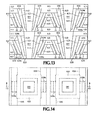
- FIGS. 9 and 10 schematically depict an embodiment of a memory structure that includes memory cells each including a memory storage element 23 disposed between a conductive tub 333 and an edge of a horizontal conductive plate 339a.
- a non-horizontal conductive panel 339b is connected to and laterally adjacent the horizontal conductive plate 339a, and a control element 25 is disposed between a face of the non-horizontal conductive panel 339b and a conductor 335 that is laterally adjacent the non-horizontal conductive panel 339b.
- a vertical conductive via or pillar 341 is nested in the interior of the conductive tub 333 and passes through an aperture in the base of the conductive tub 333.
- the conductive pillar 341 and the conductive tub 333 form a conductive structure having a vertical extent.
- the conductive tub 333 can be omitted such that the memory storage element 23 is disposed between the conductive pillar 341 and the horizontal conductive plate 339a.
- memory cells can be formed on opposite sides of a conductive tub 333.
- the memory cells can be formed in layers wherein a layer includes horizontally arranged conductive pillars 341 and memory cells, and wherein the layers are stacked so that corresponding conductive pillars 341 of different layers are stacked to form columns of conductive pillars 341.
- the columns of conductive pillars 341 can be vertical memory selection lines of a cubic memory structure, while the conductors 335 can be row memory selection lines.
- the memory storage element 23 can be formed of an oxide of the laterally contiguous horizontal plate 339a while the control element 25 can be formed of an oxide of the laterally contiguous conductor 335.
- the memory storage element 23 can be formed of an oxide that is different from an oxide of the horizontal plate 339a
- the control element 25 can be formed of an oxide that is different from an oxide of the conductor 335.
- the memory storage element 23 can also be a portion of an unpatterned oxide layer that can be a deposited oxide layer or a completely oxidized deposited metal layer, for example.
- the control element 25 can be a portion of an unpatterned oxide layer that can be a deposited oxide layer or a completely oxidized deposited metal layer, for example.
- FIGS. 11 and 12 schematically depict an embodiment of a memory structure that includes memory cells each including a memory storage element 23 disposed between a conductive tub 433 and an edge of a horizontal conductive plate 439a.
- a non-horizontal conductive panel 439b is connected to and laterally adjacent the horizontal conductive plate 439a, and a control element 25 is disposed between a face of the non-horizontal conductive panel 439b and a conductor 435 that is laterally adjacent the non-horizontal conductive panel 439b.
- a conductive via or pillar 441 is nested in the interior of the conductive tub 433 and passes through an aperture in the base of the conductive tub 433.
- the conductive pillar 441 and the conductive tub 433 form a conductive structure having a vertical extent.
- the conductive tub 433 can be omitted such that the memory storage element 23 is disposed between the conductive pillar 441 and the horizontal conductive plate 439a.
- memory cells can be formed on opposite sides of a conductive tub 433.
- the memory cells can be formed in layers wherein a layer includes horizontally arranged conductive pillars 441 and memory cells, and wherein the layers are stacked so that corresponding conductive pillars 441 of different layers are stacked to form columns of conductive pillars 441.
- the columns of conductive pillars 441 can be vertical memory selection lines of a cubic memory structure, while the conductors 435 can be row memory selection lines.
- the memory storage element 23 can be formed of an oxide of the laterally contiguous horizontal plate 439a while the control element 25 can be formed of an oxide of the laterally contiguous conductor 435.
- the memory storage element 23 can be formed of an oxide that is different from an oxide of the horizontal plate 439a, and the control element 25 can be formed of an oxide that is different from an oxide of the conductor 435.
- the memory storage element 23 can also be a portion of an unpatterned oxide layer that can be a deposited oxide layer or a completely oxidized deposited metal layer, for example.
- the control element 25 can be a portion of an unpatterned oxide layer that can be a deposited oxide layer or a completely oxidized deposited metal layer, for example.
- FIGS. 13 and 14 schematically depict an embodiment of a memory structure that includes memory cells each including a memory storage element 23 disposed between a conductive well or tub 633 and an edge of a horizontal conductive plate 639a.
- a non-horizontal conductive panel 639b is connected to and laterally adjacent the horizontal plate 639a, and a control element 25 is disposed between a face of the panel 639b and a face of an elongated conductive wall 635 that has a vertical extent and is laterally and laminarly adjacent the conductive panel 639b.
- a vertical conductive via or pillar 641 is disposed in the conductive tub 633 and contacts the tub at an opening in the base of the conductive tub, for example.
- the conductive pillar 641 and the conductive tub 633 form a conductive structure having a vertical extent.
- the conductive tub 633 can be omitted such that the memory storage element 23 is disposed between the conductive pillar 641 and the horizontal conductive plate 639a.
- memory cells can be formed on opposite sides of a conductive tub 633.
- the memory cells can be formed in layers wherein a layer includes horizontally arranged conductive tubs 633 and memory cells, and wherein the layers are stacked so that corresponding conductive pillars 641 of different layers are stacked to form columns of conductive pillars 641.
- the columns of conductive pillars 641 can be vertical memory selection lines of a cubic memory structure, while the elongated conductive walls 635 can be row memory selection lines.
- the memory storage element 23 can be formed of an oxide of the laterally contiguous horizontal plate 639a while the control element 25 can be formed of an oxide of the laterally contiguous conductor 635.
- the memory storage element 23 can be formed of an oxide that is different from an oxide of the horizontal plate 639a
- the control element 25 can be formed of an oxide that is different from an oxide of the elongated conductive wall 635.
- the memory storage element 23 can also be a portion of an unpatterned oxide layer that can be a deposited oxide layer or a completely oxidized deposited metal layer, for example.
- the control element 25 can be a portion of an unpatterned oxide layer that can be a deposited oxide layer or a completely oxidized deposited metal layer, for example.
- FIG. 15 is a block diagram of a memory carrier 70 that incorporates at least one embodiment of the invention.
- the memory carrier represents any of standard or proprietary memory card formats such as PCMCIA, PC card, Smart memory, Memory Stick, digital film, ATA, and compact flash, to name a few.
- the memory carrier 70 includes a mechanical interface 71 that provides for mechanical and electrical connection with a particular connector for the type of memory carrier implemented.
- An optional electrical interface 73 makes electrical coupling with the electrical contacts on the mechanical connector 71 and provides for example security, address decoding, voltage translation, write protection, or other typical interface functions with a set of memory ICs 80 that incorporate at least one embodiment of the invention.
- a carrier 75 typically is used to physically support the memory ICs 80, electrical interface 73, and mechanical interface 71. It will be appreciated by those skilled in the art that some electrical devices might incorporate the functionality of the electrical interface 73, thereby obviating its need in the memory carrier 70.
- FIG. 16 is a block diagram of an electronic device, in this example a computer system 90, that incorporates at least one embodiment of the invention.
- a microprocessor 91 is coupled to a memory circuit 93 used to store computer executable instructions and/or user data.
- Exemplary memory circuits 93 include BIOS memory, random access memory (RAM), read only memory (ROM) and various levels of internal or external cache memory.
- the microprocessor 91 is also connected to a storage device 95 such as a hard disk drive, floppy drive, CD/DVD drive, tape drive or other mass storage devices such as those that incorporate semiconductor memory ICs that utilize the invention.
- the microprocessor 91 can include an internal cache memory that uses the invention.
- the memory 93 may also include memory ICs that use the invention.
- the microprocessor is further connected to a display device 97 that can also incorporate memory ICs that utilize the invention.
- the electronic device can also be configured to accept the memory carrier 70 of FIG. 19.
- the disclosed memory structures can be implemented using semiconductor equipment.
- the conductors can be formed by deposition of a metal layer followed by patterning by photolithographic masking and etching.
- Dielectric regions can be formed by deposition of dielectric material, while oxide layers can be formed by deposition of an oxide, deposition of a metal followed by oxidation of the deposited metal, or oxidation of a metal feature.
- Chemical mechanical polishing (CMP) can be employed to planarize and/or expose desired regions.
- damascene processes such as dual damascene can be employed. In dual damascene processes, ILD is etched, metal is deposited on the etched ILD, and CMP is performed.
- a first electrode is created for example by depositing and patterning a metal layer to form the conductor 35, the conductive lines 135, or the conductors 235.
- a control element of a predetermined device type is formed on the first electrode, for example by oxidizing the electrode or forming an unpatterned oxide layer as described above.
- a second electrode is created, for example by depositing and patterning a metal layer to form an appropriate conductor.
- a memory storage element of the predetermined device type is formed on the second electrode, for example by oxidizing the electrode or forming an unpatterned oxide layer as described above.
- the memory storage element has a memory cross-sectional area that is smaller than the cross-sectional area of the control element.
Landscapes
- Semiconductor Memories (AREA)
- Mram Or Spin Memory Techniques (AREA)
Abstract
Description
- As computer and other electrical equipment continue to drop in price, the manufacturers of storage devices, such as memory devices and hard drives, are forced to lower the cost of their components. At the same time, computer, video game, television and other electrical device markets are requiring increasingly larger amounts of memory to store images, photographs, videos, movies, music and other storage intensive data. Thus, besides reducing cost, manufacturers of storage devices must also increase the storage density of their devices. This trend of increasing memory storage density while reducing cost required to create the storage has been on-going for many years, and even optical storage such as CD-ROM, CD-R, CD-R/W, DVD, and DVD-R variants are being challenged by device size limitations and cost. There is accordingly a need for economical, high capacity memory structures.
- The features and advantages of the disclosure will readily be appreciated by persons skilled in the art from the following detailed description when read in conjunction with the drawing wherein:
- FIG. 1 is a schematic diagram of an embodiment of a cross-point memory array in which the disclosed memory cell structures can be utilized.
- FIG. 2 is a schematic block diagram of an embodiment of a memory cell that includes a memory storage element and a control element for the memory storage element.
- FIG. 3 is a sectional view and FIG. 4 is a plan view that schematically depict an embodiment of a memory structure that includes a memory storage element and a control element that has a cross-sectional area that is larger than a cross-sectional area of the memory storage element.
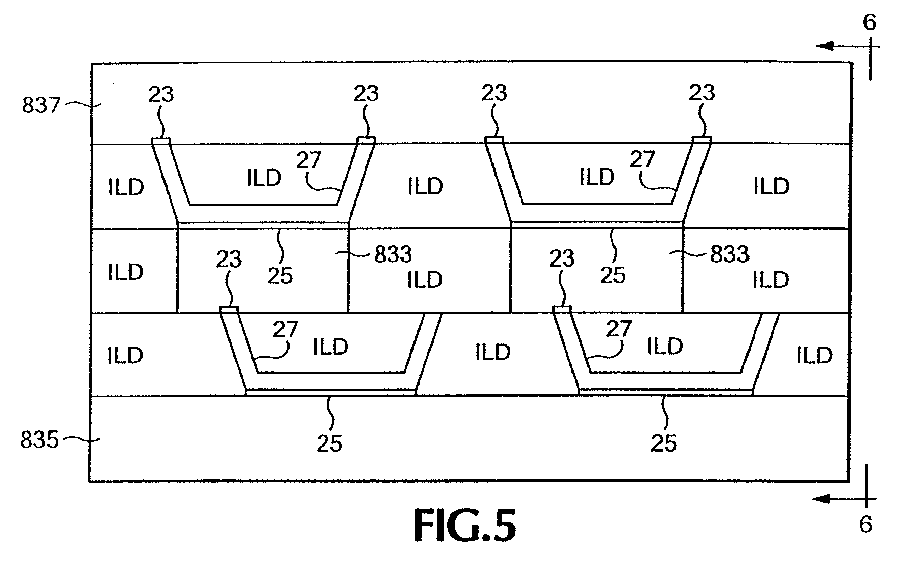
- FIGS. 5 and 6 are sectional views that schematically depict another embodiment of a memory structure that includes that includes a memory storage element and a control element that has a cross-sectional area that is larger than a cross-sectional area of the memory storage element.
- FIG. 7 is a sectional view and FIG. 8 is a plan view that schematically depict another embodiment of a memory structure that includes that includes a memory storage element and a control element that has a cross-sectional area that is larger than a cross-sectional area of the memory storage element.
- FIG. 9 is a sectional view and FIG. 10 is a plan view that schematically depict a further embodiment of a memory structure that includes that includes a memory storage element and a control element that has a cross-sectional area that is larger than a cross-sectional area of the memory storage element.
- FIG. 11 is a sectional view and FIG. 12 is a plan view that schematically depict a further embodiment of a memory structure that includes that includes a memory storage element and a control element that has a cross-sectional area that is larger than a cross-sectional area of the memory storage element.
- FIG. 13 is a sectional view and FIG. 14 is a plan view that schematically depict another embodiment of a memory structure that includes that includes a memory storage element and a control element that has a cross-sectional area that is larger than a cross-sectional area of the memory storage element.
- FIG. 15 is a schematic block diagram of an embodiment of a memory carrier that incorporates at least one of the disclosed memory cells.
- FIG. 16 is a schematic block diagram of an embodiment of an electronic device, such as a computer system, that incorporates at least one of the disclosed memory cells.
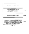
- FIG. 17 is a flow diagram of an example of an embodiment of a process for making the disclosed memory structures.
-
- FIG. 1 is a simplified schematic diagram of an embodiment of a
cross-point memory array 10 in which the disclosed memory cell structures can be utilized. Thememory arrangement 10 includes row selection conductor lines R0, R1, R2 and column selection conductor lines C0, C1, C2. Amemory cell 20 is connected between each row selection conductor line R0, R1, R2 and each column selection conductor line C0, C1, C2. It should be appreciated that the row selection conductor lines and the column selection conductor lines are referred to by "row" and "column" terminology for convenience, and that in actual implementations thememory cells 20 do not necessarily have to be physically arranged in rows and columns. Each memory cell is basically uniquely accessed or selected by a first selection line and a second selection line that can be oriented in different ways. Also, the column lines do not have to be orthogonal to the row lines, but are illustrated in that manner for ease of understanding. - FIG. 2 is a simplified electrical block diagram of an embodiment of the
memory cell 20 which includes amemory storage element 23 that is electrically connected to acontrol element 25 by an electrode E2. Thememory storage element 23 and thecontrol element 25 are serially connected between an electrode E1 and an electrode E3. The electrodes E1-E3 comprise conductive elements such as conductors, conductive regions or other conductive features, and it should be appreciated that the electrode E2 can comprise one or more electrically conductive elements. - The
memory storage element 23 is configured as a change state memory storage element, while thecontrol element 25 is configured as a control element for the change state memory storage element and provides current to the memory storage element. More particularly, the memory storage element is configured to predictably and reliably break down at a lower energy level than the control element, while the control tunnel junction region is configured for sustained operation as a control element for the memory. - Each of the
memory storage element 23 and thecontrol element 25 includes a cross-sectional area through which current flows. For example, such area can be defined by the overlap of the interfaces between the element and the electrodes on either side of the element. In the memory structures disclosed herein, thecontrol element 25 and thememory element 23 can be of the same device type, and thecontrol element 25 has a cross-sectional area that is greater than the cross-sectional area of the memory storage element, for example such that the memory storage element will break down at a lower energy level than the control element. In other words, the ratio between the control element cross-sectional area and the memory storage element cross-sectional area can be selected so that the memory storage element functions as a state change memory storage element, while the control element has control element cross-sectional area configured for sustained operation as a control element for the memory storage element. Thus, thememory storage element 23 changes state at a lower energy level than thecontrol element 25, which allows the memory storage element to be programmed. In this manner, a memory cell is programmed by selectively providing sufficient energy to the cell to cause the memory storage element to break down. A memory cell is read by providing a lesser amount of energy to cell and sensing whether current flows through the cell. - By way of illustrative example, the ratio between the cross-sectional area of the control element and the cross-sectional area of the memory storage element can be in the range of about 2 to 20.
- The
memory storage element 23 can be an antifuse device, such as a programmable tunnel junction device. The antifuse device can be either a dielectric rupture type device or a tunnel junction device. The tunnel junction can be formed from oxidized metal, thermally grown oxide, or deposited oxides or nitrides. The memory storage element may also be embodied with semiconductor materials such as polysilicon, polycrystalline silicon, amorphous silicon, microcrystalline silicon, metal filament electro migration, trap induced hysterisis, ferroelectric capacitor, Hall effect, and polysilicon resistors. Other embodiments of the memory storage element include tunneling magneto-resistive or capacitive elements as floating gates. Still further, the memory storage element can be a read only LeComber or silicide switch or a re-writable phase-change material including a write-erase-write phase change material. The memory storage element can also comprise a PIN diode or a Schottky diode. - The
control element 25 can comprise a tunnel junction device or PN, PIN or Schottky diodes. Other diodes that can be used include Zener diodes, avalanche diodes, tunnel diodes, and a four layer diode such as a silicon controlled rectifier. Also, thecontrol element 25 can be a junction field effect or bipolar transistor. Thecontrol element 25 is sized sufficiently to carry an adequate current such that the state of thestorage element 23 can be changed. When the control element is a diode, it can be formed using doped polysilicon, amorphous silicon, or microcrystalline silicon. - The
memory storage element 23 and the control element can also be of the same device type, wherein both can comprise tunnel junction devices, Schottky diodes, or PIN diodes, for example. - For conciseness, the disclosed memory structures are described as employing tunnel junction devices as the memory storage elements and control elements, and it should be appreciated that the memory storage elements and control elements can be implemented as described previously.
- By way of illustrative examples, the disclosed memory structures will be shown as integrated circuits that include interlayer dielectric such as silicon dioxide, silicon nitride, or TEOS (tetraethylorthosilicate) that provide support and isolation between various structures of an integrated circuit. The ILD can be deposited using several different technologies such as chemical vapor deposition (CVD), atmospheric pressure CVD, low pressure CVD, plasma enhanced CVD, physical vapor deposition (PVD), and sputtering. For convenience, regions and layers of such dielectric are identified in the drawings by the reference designation ILD.
- FIGS. 3 and 4 schematically depict an embodiment of a memory cell that includes a
memory storage element 23 disposed on afirst conductor 33. Acontrol element 25 is disposed on asecond conductor 35 that is laterally or transversely adjacent thefirst conductor 33. Thememory storage element 23 and thecontrol element 25 are thus horizontally, transversely or laterally separated and each can have a generally horizontal planar extent. The first andsecond conductors memory storage element 23 and thecontrol element 25 can also be substantially co-planar. Adielectric layer 41 is disposed over the first andsecond conductors openings memory storage element 23 and thecontrol element 25. Aconductive layer 37 is disposed on thedielectric layer 41 and extends into theopenings memory storage element 23 and thecontrol element 25. - The
memory storage element 23 can be formed of an oxide of thefirst conductor 33, while thecontrol element 25 can be formed of an oxide of the underlyingsecond conductor 35. Alternatively, thememory storage element 23 can be formed of an oxide that is different from an oxide of thefirst conductor 33, and thecontrol element 25 can be formed of an oxide that is different from an oxide of thesecond conductor 35. Thememory storage element 23 can also be a portion of an unpatterned oxide layer that can be a deposited oxide layer or a completely oxidized deposited metal layer, for example. Similarly, thecontrol element 25 can be a portion of an unpatterned oxide layer that can be a deposited oxide layer or a completely oxidized deposited metal layer, for example. - FIGS. 5 and 6 schematically depict an embodiment of a memory structure that includes a plurality of memory cells each including a
memory storage element 23 disposed between the rim edge of a conductive well ortub 27 and aconductor control element 25 disposed between the base of theconductive tub 27 and aconductor memory storage element 23 and/or thecontrol element 25 can have a horizontally planar extent, and are vertically separated. - The memory cells of FIGS. 5 and 6 can be implemented in stacked layers for example wherein a
conductor 833 that is vertically adjacent the rim edge of a givenconductive tub 27 is vertically adjacent the base of aconductive tub 27 that is in an adjacent layer. - By way of illustrative example, the
conductor 833 can be a row selection line while theconductors conductive tub 27 can be laterally offset relative to theconductor 833 that is vertically adjacent the rim of suchconductive tub 27, for example to control the area of the memory tunneljunction oxide region 23. As a result, aconductive tub 27 is laterally offset relative to another vertically adjacentconductive tub 27 in an adjacent layer. - The
memory storage element 23 can formed of an oxide of theconductive tub 27, and thecontrol element 25 can be formed of an oxide of theconductor conductive tub 27. Alternatively, the memory tunneljunction oxide region 23 can be formed of an oxide that is different from an oxide of the rim of theconductive tub 27, and the control tunneljunction oxide region 25 can be formed of an oxide that is different from an oxide of theconductor memory storage element 23 can also be a portion of an unpatterned oxide layer that can be a deposited oxide layer or a completely oxidized deposited metal layer, for example. Similarly, thecontrol element 25 can be a portion of an unpatterned oxide layer that can be a deposited oxide layer or a completely oxidized deposited metal layer, for example. - FIGS. 7 and 8 schematically depict an embodiment of a memory structure that includes memory cells each including a
memory storage element 23 disposed between a conductive well ortub 133 and a conductive region or block 139 that is laterally adjacent theconductive tub 133. Acontrol element 25 is disposed between theconductive block 139 and aconductor 135 that is laterally adjacent theconductive block 139. Thememory storage element 23 and thecontrol element 25 of a memory cell of FIGS. 5 and 6 are thus horizontally separated and each can be planar with a vertical extent. Theconductive block 139 can be a truncated wedge, and thememory storage element 23 and thecontrol element 25 are in contact with opposing faces of the truncated wedge. A vertical conductive via orpillar 141 is disposed in theconductive well 133, and can extend through an aperture in the base of theconductive tub 133. Theconductive pillar 141 and theconductive tub 133 form a conductive structure having a vertical extent. Theconductive tub 133 can be omitted such that thememory storage element 23 is disposed between theconductive pillar 141 and theconductive block 139. - As shown in FIGS. 7 and 8, memory cells can be formed on opposite sides of a
conductive tub 133. Also, the memory cells can be formed in layers wherein a layer includes horizontally arrangedconductive tubs 133 and memory cells, and wherein the layers are stacked so that correspondingconductive pillars 141 of different layers are stacked to form columns ofconductive pillars 141. The columns ofconductive pillars 141 can comprise vertical memory selection lines of a cubic memory structure, while theconductors 135 can comprise row memory selection lines. In a cubic memory structure, row and column memory selection lines are arranged in a 3-D structure, for example as disclosed in commonly assigned, co-pending U.S. application Serial No. , filed concurrently herewith on , attorney docket number 10018288. - The
memory storage element 23 can formed of an oxide of the laterally contiguousconductive block 139 while thecontrol element 25 can be formed of an oxide of the laterallycontiguous conductor 135. Alternatively, thememory storage element 23 can be formed of an oxide that is different from an oxide of theconductive block 139, and thecontrol element 25 can be formed of an oxide that is different from an oxide of theconductor 135. Thememory storage element 23 can also be a portion of an unpatterned oxide layer that can be a deposited oxide layer or a completely oxidized deposited metal layer, for example. Similarly, thecontrol element 25 can be a portion of an unpatterned oxide layer that can be a deposited oxide layer or a completely oxidized deposited metal layer, for example. - FIGS. 9 and 10 schematically depict an embodiment of a memory structure that includes memory cells each including a
memory storage element 23 disposed between aconductive tub 333 and an edge of a horizontalconductive plate 339a. A non-horizontalconductive panel 339b is connected to and laterally adjacent the horizontalconductive plate 339a, and acontrol element 25 is disposed between a face of the non-horizontalconductive panel 339b and aconductor 335 that is laterally adjacent the non-horizontalconductive panel 339b. A vertical conductive via orpillar 341 is nested in the interior of theconductive tub 333 and passes through an aperture in the base of theconductive tub 333. Theconductive pillar 341 and theconductive tub 333 form a conductive structure having a vertical extent. Theconductive tub 333 can be omitted such that thememory storage element 23 is disposed between theconductive pillar 341 and the horizontalconductive plate 339a. - As shown in FIGS. 9 and 10, memory cells can be formed on opposite sides of a
conductive tub 333. Also, the memory cells can be formed in layers wherein a layer includes horizontally arrangedconductive pillars 341 and memory cells, and wherein the layers are stacked so that correspondingconductive pillars 341 of different layers are stacked to form columns ofconductive pillars 341. The columns ofconductive pillars 341 can be vertical memory selection lines of a cubic memory structure, while theconductors 335 can be row memory selection lines. - The
memory storage element 23 can be formed of an oxide of the laterally contiguoushorizontal plate 339a while thecontrol element 25 can be formed of an oxide of the laterallycontiguous conductor 335. Alternatively, thememory storage element 23 can be formed of an oxide that is different from an oxide of thehorizontal plate 339a, and thecontrol element 25 can be formed of an oxide that is different from an oxide of theconductor 335. Thememory storage element 23 can also be a portion of an unpatterned oxide layer that can be a deposited oxide layer or a completely oxidized deposited metal layer, for example. Similarly, thecontrol element 25 can be a portion of an unpatterned oxide layer that can be a deposited oxide layer or a completely oxidized deposited metal layer, for example. - FIGS. 11 and 12 schematically depict an embodiment of a memory structure that includes memory cells each including a
memory storage element 23 disposed between aconductive tub 433 and an edge of a horizontalconductive plate 439a. A non-horizontalconductive panel 439b is connected to and laterally adjacent the horizontalconductive plate 439a, and acontrol element 25 is disposed between a face of the non-horizontalconductive panel 439b and aconductor 435 that is laterally adjacent the non-horizontalconductive panel 439b. A conductive via orpillar 441 is nested in the interior of theconductive tub 433 and passes through an aperture in the base of theconductive tub 433. Theconductive pillar 441 and theconductive tub 433 form a conductive structure having a vertical extent. Theconductive tub 433 can be omitted such that thememory storage element 23 is disposed between theconductive pillar 441 and the horizontalconductive plate 439a. - As shown in FIGS. 11 and 12, memory cells can be formed on opposite sides of a
conductive tub 433. Also, the memory cells can be formed in layers wherein a layer includes horizontally arrangedconductive pillars 441 and memory cells, and wherein the layers are stacked so that correspondingconductive pillars 441 of different layers are stacked to form columns ofconductive pillars 441. The columns ofconductive pillars 441 can be vertical memory selection lines of a cubic memory structure, while theconductors 435 can be row memory selection lines. - The
memory storage element 23 can be formed of an oxide of the laterally contiguoushorizontal plate 439a while thecontrol element 25 can be formed of an oxide of the laterallycontiguous conductor 435. Thememory storage element 23 can be formed of an oxide that is different from an oxide of thehorizontal plate 439a, and thecontrol element 25 can be formed of an oxide that is different from an oxide of theconductor 435. Thememory storage element 23 can also be a portion of an unpatterned oxide layer that can be a deposited oxide layer or a completely oxidized deposited metal layer, for example. Similarly, thecontrol element 25 can be a portion of an unpatterned oxide layer that can be a deposited oxide layer or a completely oxidized deposited metal layer, for example. - FIGS. 13 and 14 schematically depict an embodiment of a memory structure that includes memory cells each including a
memory storage element 23 disposed between a conductive well ortub 633 and an edge of a horizontalconductive plate 639a. A non-horizontalconductive panel 639b is connected to and laterally adjacent thehorizontal plate 639a, and acontrol element 25 is disposed between a face of thepanel 639b and a face of an elongatedconductive wall 635 that has a vertical extent and is laterally and laminarly adjacent theconductive panel 639b. A vertical conductive via orpillar 641 is disposed in theconductive tub 633 and contacts the tub at an opening in the base of the conductive tub, for example. Theconductive pillar 641 and theconductive tub 633 form a conductive structure having a vertical extent. Theconductive tub 633 can be omitted such that thememory storage element 23 is disposed between theconductive pillar 641 and the horizontalconductive plate 639a. - As shown in FIGS. 13 and 14, memory cells can be formed on opposite sides of a
conductive tub 633. Also, the memory cells can be formed in layers wherein a layer includes horizontally arrangedconductive tubs 633 and memory cells, and wherein the layers are stacked so that correspondingconductive pillars 641 of different layers are stacked to form columns ofconductive pillars 641. The columns ofconductive pillars 641 can be vertical memory selection lines of a cubic memory structure, while the elongatedconductive walls 635 can be row memory selection lines. - The
memory storage element 23 can be formed of an oxide of the laterally contiguoushorizontal plate 639a while thecontrol element 25 can be formed of an oxide of the laterallycontiguous conductor 635. Alternatively, thememory storage element 23 can be formed of an oxide that is different from an oxide of thehorizontal plate 639a, and thecontrol element 25 can be formed of an oxide that is different from an oxide of the elongatedconductive wall 635. Thememory storage element 23 can also be a portion of an unpatterned oxide layer that can be a deposited oxide layer or a completely oxidized deposited metal layer, for example. Similarly, thecontrol element 25 can be a portion of an unpatterned oxide layer that can be a deposited oxide layer or a completely oxidized deposited metal layer, for example. - FIG. 15 is a block diagram of a
memory carrier 70 that incorporates at least one embodiment of the invention. The memory carrier represents any of standard or proprietary memory card formats such as PCMCIA, PC card, Smart memory, Memory Stick, digital film, ATA, and compact flash, to name a few. Thememory carrier 70 includes amechanical interface 71 that provides for mechanical and electrical connection with a particular connector for the type of memory carrier implemented. An optionalelectrical interface 73 makes electrical coupling with the electrical contacts on themechanical connector 71 and provides for example security, address decoding, voltage translation, write protection, or other typical interface functions with a set ofmemory ICs 80 that incorporate at least one embodiment of the invention. Acarrier 75, for example a printed circuit board or ceramic substrate, typically is used to physically support thememory ICs 80,electrical interface 73, andmechanical interface 71. It will be appreciated by those skilled in the art that some electrical devices might incorporate the functionality of theelectrical interface 73, thereby obviating its need in thememory carrier 70. - FIG. 16 is a block diagram of an electronic device, in this example a
computer system 90, that incorporates at least one embodiment of the invention. In particular for a computer system, several different electrical devices as shown may be incorporated into the package. For example, amicroprocessor 91 is coupled to amemory circuit 93 used to store computer executable instructions and/or user data.Exemplary memory circuits 93 include BIOS memory, random access memory (RAM), read only memory (ROM) and various levels of internal or external cache memory. Themicroprocessor 91 is also connected to astorage device 95 such as a hard disk drive, floppy drive, CD/DVD drive, tape drive or other mass storage devices such as those that incorporate semiconductor memory ICs that utilize the invention. Themicroprocessor 91 can include an internal cache memory that uses the invention. Thememory 93 may also include memory ICs that use the invention. The microprocessor is further connected to adisplay device 97 that can also incorporate memory ICs that utilize the invention. The electronic device can also be configured to accept thememory carrier 70 of FIG. 19. - The disclosed memory structures can be implemented using semiconductor equipment. For example, the conductors can be formed by deposition of a metal layer followed by patterning by photolithographic masking and etching. Dielectric regions can be formed by deposition of dielectric material, while oxide layers can be formed by deposition of an oxide, deposition of a metal followed by oxidation of the deposited metal, or oxidation of a metal feature. Chemical mechanical polishing (CMP) can be employed to planarize and/or expose desired regions. Also, damascene processes such as dual damascene can be employed. In dual damascene processes, ILD is etched, metal is deposited on the etched ILD, and CMP is performed.
- Referring now to FIG. 17, the disclosed structures can generally be made as follows. At 101 a first electrode is created for example by depositing and patterning a metal layer to form the
conductor 35, theconductive lines 135, or the conductors 235. At 103 a control element of a predetermined device type is formed on the first electrode, for example by oxidizing the electrode or forming an unpatterned oxide layer as described above. At 105 a second electrode is created, for example by depositing and patterning a metal layer to form an appropriate conductor. At 107 a memory storage element of the predetermined device type is formed on the second electrode, for example by oxidizing the electrode or forming an unpatterned oxide layer as described above. The memory storage element has a memory cross-sectional area that is smaller than the cross-sectional area of the control element. - Although the foregoing has been a description and illustration of specific embodiments of the invention, various modifications and changes thereto can be made by persons skilled in the art without departing from the scope and spirit of the invention as defined by the following claims.
Claims (20)
- A memory structure comprising:a first electrode (35, 835, 135, 335, 435, 635);a second electrode (37, 27, 139a, 139b, 339a, 339b, 439a, 439b, 639a, 639b);a third electrode (33, 833, 133, 141, 333, 341, 433, 441, 633, 641);a memory storage element (23) of a predetermined device type disposed between said third electrode and said second electrode, said memory storage element having a memory storage element cross-sectional area and configured for predictable breakdown as a memory storage element;a control element (25) of said predetermined device type disposed between said second electrode and said first electrode, said control element having a control cross-sectional area and configured as a control element for said memory storage element; andsaid control element cross-sectional area being larger than said memory storage element cross-sectional area.
- The memory structure of claim 1 wherein:said first electrode comprises a first conductor having a top surface;said third electrode comprises a second conductor horizontally adjacent said first conductor and having a top surface;said control element is disposed on said top surface of said first conductor; andsaid memory storage element is disposed on said top surface of said second conductor.
- The memory structure of claim 1 wherein said third electrode comprises a conductive structure having a vertical extent.
- The memory structure of claim 1 wherein said third electrode comprises a conductive tub.
- The memory structure of claim 1 wherein said third electrode comprises a conductive pillar.
- The memory structure of claim 1 wherein said third electrode comprises a truncated conductive cone.
- The memory structure of claim 1 wherein said second electrode comprises a conductive plate.
- The memory structure of claim 1 wherein said second electrode comprises a conductive tub.
- The memory structure of claims 1, 2, 3, 4, 5, 6, 7 or 8 wherein said memory storage element comprises a tunnel junction device.
- The memory structure of claims 1, 2, 3, 4, 5, 6, 7 or 8 wherein said memory storage element comprises an oxide of said second electrode.
- The memory structure of claims 1, 2, 3, 4, 5, 6, 7 or 8 wherein said memory storage element comprises an oxide that is different from an oxide of said second electrode.
- The memory structure of claim 1, 2, 3, 4, 5, 6, 7 or 8 wherein said memory storage element is selected from the group consisting of an antifuse, a fuse, a charge storage device, a resistive material, a trap-induced hysteresis material, a ferroelectric capacitor material, a Hall effect material, and a tunneling magneto-resistive material.
- The memory structure of claim 1, 2, 3, 4, 5, 6, 7 or 8 wherein said memory storage element comprises a re-writable phase change material.
- The memory structure of claim 1, 2, 3, 4, 5, 6, 7 or 8 wherein said control element comprises a tunnel junction device.
- The memory structure of claim 1, 2, 3, 4, 5, 6, 7 or 8 wherein said control element comprises an oxide of said first electrode.
- The memory structure of claim 1, 2, 3, 4, 5, 6, 7 or 8 wherein said control element comprises an oxide that is different from an oxide of said first electrode.
- An electronic device configured to receive the memory structure of claims 1, 2, 3, 4, 5, 6, 7 or 8.
- An electronic device including the memory structure of claims 1, 2, 3, 4, 5, 6, 7 or 8.
- A memory structure comprising:a plurality of layers of memory cells;each memory cell comprising a first electrode (835, 135, 335, 435, 635), a second electrode (27, 139a, 139b, 339a, 339b, 439a, 439b, 639a, 639b), a memory storage element (23) disposed between said second electrode and said third electrode, and a control element (25) disposed between said first electrode and said second electrode; andsaid control element having a cross-sectional area that is greater than a cross-sectional area of said memory storage element.
- A method of making a memory structure comprising:creating a first electrode;forming on the first electrode a control element of a predetermined device type on the first electrode;creating a second electrode; andforming a memory storage element of the predetermined device type and having a cross-sectional area that is smaller than a cross-sectional area of the control element.
Applications Claiming Priority (2)
| Application Number | Priority Date | Filing Date | Title |
|---|---|---|---|
| US10/116,497 US6967350B2 (en) | 2002-04-02 | 2002-04-02 | Memory structures |
| US116497 | 2002-04-02 |
Publications (1)
| Publication Number | Publication Date |
|---|---|
| EP1351306A2 true EP1351306A2 (en) | 2003-10-08 |
Family
ID=28041088
Family Applications (1)
| Application Number | Title | Priority Date | Filing Date |
|---|---|---|---|
| EP03252042A Withdrawn EP1351306A2 (en) | 2002-04-02 | 2003-03-31 | Memory structures |
Country Status (7)
| Country | Link |
|---|---|
| US (2) | US6967350B2 (en) |
| EP (1) | EP1351306A2 (en) |
| JP (1) | JP2004006777A (en) |
| KR (1) | KR20030079732A (en) |
| CN (1) | CN1452248A (en) |
| DE (1) | DE60324725D1 (en) |
| TW (1) | TW200305273A (en) |
Cited By (1)
| Publication number | Priority date | Publication date | Assignee | Title |
|---|---|---|---|---|
| EP1455390A3 (en) * | 2003-03-05 | 2008-10-15 | Hewlett-Packard Development Company, L.P. | Buried magnetic tunnel-junction memory cell and methods for fabricating |
Families Citing this family (18)
| Publication number | Priority date | Publication date | Assignee | Title |
|---|---|---|---|---|
| US6967350B2 (en) * | 2002-04-02 | 2005-11-22 | Hewlett-Packard Development Company, L.P. | Memory structures |
| US6821848B2 (en) * | 2002-04-02 | 2004-11-23 | Hewlett-Packard Development Company, L.P. | Tunnel-junction structures and methods |
| US6858883B2 (en) * | 2003-06-03 | 2005-02-22 | Hewlett-Packard Development Company, L.P. | Partially processed tunnel junction control element |
| US7095644B2 (en) * | 2003-12-22 | 2006-08-22 | Unity Semiconductor Corporation | Conductive memory array having page mode and burst mode read capability |
| US7099179B2 (en) * | 2003-12-22 | 2006-08-29 | Unity Semiconductor Corporation | Conductive memory array having page mode and burst mode write capability |
| DE102004014435A1 (en) * | 2004-03-24 | 2005-11-17 | Siemens Ag | Arrangement with an integrated circuit |
| US7485540B2 (en) * | 2005-08-18 | 2009-02-03 | International Business Machines Corporation | Integrated BEOL thin film resistor |
| KR100764056B1 (en) * | 2006-09-14 | 2007-10-08 | 삼성전자주식회사 | Phase change memory device and manufacturing method thereof |
| KR101046852B1 (en) | 2006-10-16 | 2011-07-06 | 파나소닉 주식회사 | Nonvolatile Memory and Manufacturing Method Thereof |
| US8242479B2 (en) * | 2007-11-15 | 2012-08-14 | Panasonic Corporation | Nonvolatile memory apparatus and manufacturing method thereof |
| JP5159270B2 (en) * | 2007-11-22 | 2013-03-06 | 株式会社東芝 | Nonvolatile semiconductor memory device and manufacturing method thereof |
| WO2010042732A2 (en) * | 2008-10-08 | 2010-04-15 | The Regents Of The University Of Michigan | Silicon-based nanoscale resistive device with adjustable resistance |
| KR20100041155A (en) * | 2008-10-13 | 2010-04-22 | 삼성전자주식회사 | Resistive memory device |
| US8586959B2 (en) * | 2010-04-28 | 2013-11-19 | Hewlett-Packard Development Company, L.P. | Memristive switch device |
| US20130140515A1 (en) * | 2011-02-23 | 2013-06-06 | Yoshio Kawashima | Nonvolatile memory element and method of manufacturing the same |
| CN103119717A (en) * | 2011-09-16 | 2013-05-22 | 松下电器产业株式会社 | Manufacturing method of nonvolatile memory element and nonvolatile memory element |
| CN108630810B (en) * | 2018-05-14 | 2022-07-19 | 中国科学院微电子研究所 | 1S1R memory integrated structure and preparation method thereof |
| US20250054859A1 (en) * | 2023-08-08 | 2025-02-13 | Nanya Technology Corporation | Semiconductor device and method of forming the same |
Family Cites Families (41)
| Publication number | Priority date | Publication date | Assignee | Title |
|---|---|---|---|---|
| US3271591A (en) * | 1963-09-20 | 1966-09-06 | Energy Conversion Devices Inc | Symmetrical current controlling device |
| US3530441A (en) * | 1969-01-15 | 1970-09-22 | Energy Conversion Devices Inc | Method and apparatus for storing and retrieving information |
| BE755039A (en) * | 1969-09-15 | 1971-02-01 | Ibm | PERMANENT SEMI-CONDUCTOR MEMORY |
| IL61678A (en) * | 1979-12-13 | 1984-04-30 | Energy Conversion Devices Inc | Programmable cell and programmable electronic arrays comprising such cells |
| US4499557A (en) * | 1980-10-28 | 1985-02-12 | Energy Conversion Devices, Inc. | Programmable cell for use in programmable electronic arrays |
| US5335219A (en) * | 1991-01-18 | 1994-08-02 | Ovshinsky Stanford R | Homogeneous composition of microcrystalline semiconductor material, semiconductor devices and directly overwritable memory elements fabricated therefrom, and arrays fabricated from the memory elements |
| US5625220A (en) * | 1991-02-19 | 1997-04-29 | Texas Instruments Incorporated | Sublithographic antifuse |
| US5349220A (en) * | 1993-08-10 | 1994-09-20 | United Microelectronics Corporation | Flash memory cell and its operation |
| US5485031A (en) * | 1993-11-22 | 1996-01-16 | Actel Corporation | Antifuse structure suitable for VLSI application |
| US5751012A (en) * | 1995-06-07 | 1998-05-12 | Micron Technology, Inc. | Polysilicon pillar diode for use in a non-volatile memory cell |
| US5659500A (en) * | 1995-09-26 | 1997-08-19 | Texas Instruments Incorporated | Nonvolatile memory array with compatible vertical source lines |
| US5783467A (en) * | 1995-12-29 | 1998-07-21 | Vlsi Technology, Inc. | Method of making antifuse structures using implantation of both neutral and dopant species |
| US5835396A (en) * | 1996-10-17 | 1998-11-10 | Zhang; Guobiao | Three-dimensional read-only memory |
| US6026017A (en) * | 1997-04-11 | 2000-02-15 | Programmable Silicon Solutions | Compact nonvolatile memory |
| US6002607A (en) * | 1998-02-24 | 1999-12-14 | National Semiconductor Corporation | Read-only-memory (ROM) having a memory cell that stores a plurality of bits of information |
| US6185121B1 (en) * | 1998-02-26 | 2001-02-06 | Lucent Technologies Inc. | Access structure for high density read only memory |
| US5942777A (en) * | 1998-05-05 | 1999-08-24 | Sun Microsystems, Inc. | Memory device including a memory array having a combination of trench capacitor DRAM cells and stacked capacitor DRAM cells |
| US6262487B1 (en) * | 1998-06-23 | 2001-07-17 | Kabushiki Kaisha Toshiba | Semiconductor integrated circuit device, semiconductor integrated circuit wiring method, and cell arranging method |
| US6372633B1 (en) * | 1998-07-08 | 2002-04-16 | Applied Materials, Inc. | Method and apparatus for forming metal interconnects |
| US6033955A (en) * | 1998-09-23 | 2000-03-07 | Advanced Micro Devices, Inc. | Method of making flexibly partitioned metal line segments for a simultaneous operation flash memory device with a flexible bank partition architecture |
| US6034882A (en) * | 1998-11-16 | 2000-03-07 | Matrix Semiconductor, Inc. | Vertically stacked field programmable nonvolatile memory and method of fabrication |
| US6351406B1 (en) * | 1998-11-16 | 2002-02-26 | Matrix Semiconductor, Inc. | Vertically stacked field programmable nonvolatile memory and method of fabrication |
| US6380003B1 (en) * | 1999-12-22 | 2002-04-30 | International Business Machines Corporation | Damascene anti-fuse with slot via |
| US6251710B1 (en) * | 2000-04-27 | 2001-06-26 | International Business Machines Corporation | Method of making a dual damascene anti-fuse with via before wire |
| US6888750B2 (en) * | 2000-04-28 | 2005-05-03 | Matrix Semiconductor, Inc. | Nonvolatile memory on SOI and compound semiconductor substrates and method of fabrication |
| US6515888B2 (en) * | 2000-08-14 | 2003-02-04 | Matrix Semiconductor, Inc. | Low cost three-dimensional memory array |
| JP4726292B2 (en) * | 2000-11-14 | 2011-07-20 | ルネサスエレクトロニクス株式会社 | Thin film magnetic memory device |
| US6591394B2 (en) * | 2000-12-22 | 2003-07-08 | Matrix Semiconductor, Inc. | Three-dimensional memory array and method for storing data bits and ECC bits therein |
| JP4667594B2 (en) * | 2000-12-25 | 2011-04-13 | ルネサスエレクトロニクス株式会社 | Thin film magnetic memory device |
| US6771473B2 (en) * | 2001-01-22 | 2004-08-03 | Matsushita Electric Industrial Co., Ltd. | Magnetoresistive element and method for producing the same |
| US6744086B2 (en) * | 2001-05-15 | 2004-06-01 | Nve Corporation | Current switched magnetoresistive memory cell |
| US6717215B2 (en) * | 2001-06-21 | 2004-04-06 | Hewlett-Packard Development Company, L.P. | Memory structures |
| US6576969B2 (en) * | 2001-09-25 | 2003-06-10 | Hewlett-Packard Development Company, L.P. | Magneto-resistive device having soft reference layer |
| US6534841B1 (en) * | 2001-12-14 | 2003-03-18 | Hewlett-Packard Company | Continuous antifuse material in memory structure |
| US6559516B1 (en) * | 2002-01-16 | 2003-05-06 | Hewlett-Packard Development Company | Antifuse structure and method of making |
| US6625059B1 (en) * | 2002-03-06 | 2003-09-23 | Hewlett-Packard Development Company, L.P. | Synthetic ferrimagnet reference layer for a magnetic storage device |
| US6967350B2 (en) * | 2002-04-02 | 2005-11-22 | Hewlett-Packard Development Company, L.P. | Memory structures |
| US20030183868A1 (en) * | 2002-04-02 | 2003-10-02 | Peter Fricke | Memory structures |
| US6643159B2 (en) * | 2002-04-02 | 2003-11-04 | Hewlett-Packard Development Company, L.P. | Cubic memory array |
| US6821848B2 (en) * | 2002-04-02 | 2004-11-23 | Hewlett-Packard Development Company, L.P. | Tunnel-junction structures and methods |
| US6940085B2 (en) * | 2002-04-02 | 2005-09-06 | Hewlett-Packard Development Company, I.P. | Memory structures |
-
2002
- 2002-04-02 US US10/116,497 patent/US6967350B2/en not_active Expired - Lifetime
- 2002-09-06 US US10/236,274 patent/US6711045B2/en not_active Expired - Fee Related
-
2003
- 2003-01-22 TW TW092101392A patent/TW200305273A/en unknown
- 2003-03-31 EP EP03252042A patent/EP1351306A2/en not_active Withdrawn
- 2003-03-31 DE DE60324725T patent/DE60324725D1/en not_active Expired - Lifetime
- 2003-04-01 KR KR10-2003-0020377A patent/KR20030079732A/en not_active Ceased
- 2003-04-01 JP JP2003097941A patent/JP2004006777A/en not_active Withdrawn
- 2003-04-02 CN CN03107797A patent/CN1452248A/en active Pending
Cited By (1)
| Publication number | Priority date | Publication date | Assignee | Title |
|---|---|---|---|---|
| EP1455390A3 (en) * | 2003-03-05 | 2008-10-15 | Hewlett-Packard Development Company, L.P. | Buried magnetic tunnel-junction memory cell and methods for fabricating |
Also Published As
| Publication number | Publication date |
|---|---|
| CN1452248A (en) | 2003-10-29 |
| JP2004006777A (en) | 2004-01-08 |
| US20030183849A1 (en) | 2003-10-02 |
| US20030185034A1 (en) | 2003-10-02 |
| TW200305273A (en) | 2003-10-16 |
| DE60324725D1 (en) | 2009-01-02 |
| US6967350B2 (en) | 2005-11-22 |
| KR20030079732A (en) | 2003-10-10 |
| US6711045B2 (en) | 2004-03-23 |
Similar Documents
| Publication | Publication Date | Title |
|---|---|---|
| US6940085B2 (en) | Memory structures | |
| US6967350B2 (en) | Memory structures | |
| US6707087B2 (en) | Structure of chalcogenide memory element | |
| US6781858B2 (en) | Cubic memory array | |
| US6858883B2 (en) | Partially processed tunnel junction control element | |
| US6661691B2 (en) | Interconnection structure and methods | |
| US7489551B2 (en) | Memory architecture and method of manufacture and operation thereof | |
| US6717215B2 (en) | Memory structures | |
| WO2003085734A1 (en) | Interconnection structure and methods | |
| EP1609186B1 (en) | Cubic memory array and method of manufacturing | |
| EP1351253A1 (en) | Memory structures | |
| HK1056257A (en) | Memory structures |
Legal Events
| Date | Code | Title | Description |
|---|---|---|---|
| PUAI | Public reference made under article 153(3) epc to a published international application that has entered the european phase |
Free format text: ORIGINAL CODE: 0009012 |
|
| AK | Designated contracting states |
Kind code of ref document: A2 Designated state(s): AT BE BG CH CY CZ DE DK EE ES FI FR GB GR HU IE IT LI LU MC NL PT RO SE SI SK TR |
|
| AX | Request for extension of the european patent |
Extension state: AL LT LV MK |
|
| STAA | Information on the status of an ep patent application or granted ep patent |
Free format text: STATUS: THE APPLICATION HAS BEEN WITHDRAWN |
|
| 18W | Application withdrawn |
Effective date: 20050310 |
|
| REG | Reference to a national code |
Ref country code: HK Ref legal event code: WD Ref document number: 1056257 Country of ref document: HK |