EP1351285A2 - Electrical device comprising two substrates bonded together and method of making same - Google Patents
Electrical device comprising two substrates bonded together and method of making same Download PDFInfo
- Publication number
- EP1351285A2 EP1351285A2 EP03251979A EP03251979A EP1351285A2 EP 1351285 A2 EP1351285 A2 EP 1351285A2 EP 03251979 A EP03251979 A EP 03251979A EP 03251979 A EP03251979 A EP 03251979A EP 1351285 A2 EP1351285 A2 EP 1351285A2
- Authority
- EP
- European Patent Office
- Prior art keywords
- contact
- bond
- substrates
- bonding structure
- deformation condition
- Prior art date
- Legal status (The legal status is an assumption and is not a legal conclusion. Google has not performed a legal analysis and makes no representation as to the accuracy of the status listed.)
- Withdrawn
Links
Images




Classifications
-
- H—ELECTRICITY
- H10—SEMICONDUCTOR DEVICES; ELECTRIC SOLID-STATE DEVICES NOT OTHERWISE PROVIDED FOR
- H10W—GENERIC PACKAGES, INTERCONNECTIONS, CONNECTORS OR OTHER CONSTRUCTIONAL DETAILS OF DEVICES COVERED BY CLASS H10
- H10W90/00—Package configurations
-
- B—PERFORMING OPERATIONS; TRANSPORTING
- B81—MICROSTRUCTURAL TECHNOLOGY
- B81B—MICROSTRUCTURAL DEVICES OR SYSTEMS, e.g. MICROMECHANICAL DEVICES
- B81B7/00—Microstructural systems ; Auxiliary parts of microstructural devices or systems
- B81B7/0006—Interconnects
-
- H—ELECTRICITY
- H10—SEMICONDUCTOR DEVICES; ELECTRIC SOLID-STATE DEVICES NOT OTHERWISE PROVIDED FOR
- H10W—GENERIC PACKAGES, INTERCONNECTIONS, CONNECTORS OR OTHER CONSTRUCTIONAL DETAILS OF DEVICES COVERED BY CLASS H10
- H10W76/00—Containers; Fillings or auxiliary members therefor; Seals
- H10W76/60—Seals
-
- H—ELECTRICITY
- H10—SEMICONDUCTOR DEVICES; ELECTRIC SOLID-STATE DEVICES NOT OTHERWISE PROVIDED FOR
- H10W—GENERIC PACKAGES, INTERCONNECTIONS, CONNECTORS OR OTHER CONSTRUCTIONAL DETAILS OF DEVICES COVERED BY CLASS H10
- H10W95/00—Packaging processes not covered by the other groups of this subclass
-
- H—ELECTRICITY
- H10—SEMICONDUCTOR DEVICES; ELECTRIC SOLID-STATE DEVICES NOT OTHERWISE PROVIDED FOR
- H10W—GENERIC PACKAGES, INTERCONNECTIONS, CONNECTORS OR OTHER CONSTRUCTIONAL DETAILS OF DEVICES COVERED BY CLASS H10
- H10W72/00—Interconnections or connectors in packages
- H10W72/071—Connecting or disconnecting
- H10W72/072—Connecting or disconnecting of bump connectors
-
- H—ELECTRICITY
- H10—SEMICONDUCTOR DEVICES; ELECTRIC SOLID-STATE DEVICES NOT OTHERWISE PROVIDED FOR
- H10W—GENERIC PACKAGES, INTERCONNECTIONS, CONNECTORS OR OTHER CONSTRUCTIONAL DETAILS OF DEVICES COVERED BY CLASS H10
- H10W72/00—Interconnections or connectors in packages
- H10W72/071—Connecting or disconnecting
- H10W72/072—Connecting or disconnecting of bump connectors
- H10W72/07231—Techniques
- H10W72/07236—Soldering or alloying
-
- H—ELECTRICITY
- H10—SEMICONDUCTOR DEVICES; ELECTRIC SOLID-STATE DEVICES NOT OTHERWISE PROVIDED FOR
- H10W—GENERIC PACKAGES, INTERCONNECTIONS, CONNECTORS OR OTHER CONSTRUCTIONAL DETAILS OF DEVICES COVERED BY CLASS H10
- H10W72/00—Interconnections or connectors in packages
- H10W72/071—Connecting or disconnecting
- H10W72/072—Connecting or disconnecting of bump connectors
- H10W72/07251—Connecting or disconnecting of bump connectors characterised by changes in properties of the bump connectors during connecting
- H10W72/07254—Connecting or disconnecting of bump connectors characterised by changes in properties of the bump connectors during connecting changes in dispositions
-
- H—ELECTRICITY
- H10—SEMICONDUCTOR DEVICES; ELECTRIC SOLID-STATE DEVICES NOT OTHERWISE PROVIDED FOR
- H10W—GENERIC PACKAGES, INTERCONNECTIONS, CONNECTORS OR OTHER CONSTRUCTIONAL DETAILS OF DEVICES COVERED BY CLASS H10
- H10W72/00—Interconnections or connectors in packages
- H10W72/20—Bump connectors, e.g. solder bumps or copper pillars; Dummy bumps; Thermal bumps
- H10W72/241—Dispositions, e.g. layouts
-
- H—ELECTRICITY
- H10—SEMICONDUCTOR DEVICES; ELECTRIC SOLID-STATE DEVICES NOT OTHERWISE PROVIDED FOR
- H10W—GENERIC PACKAGES, INTERCONNECTIONS, CONNECTORS OR OTHER CONSTRUCTIONAL DETAILS OF DEVICES COVERED BY CLASS H10
- H10W72/00—Interconnections or connectors in packages
- H10W72/20—Bump connectors, e.g. solder bumps or copper pillars; Dummy bumps; Thermal bumps
- H10W72/241—Dispositions, e.g. layouts
- H10W72/244—Dispositions, e.g. layouts relative to underlying supporting features, e.g. bond pads, RDLs or vias
-
- H—ELECTRICITY
- H10—SEMICONDUCTOR DEVICES; ELECTRIC SOLID-STATE DEVICES NOT OTHERWISE PROVIDED FOR
- H10W—GENERIC PACKAGES, INTERCONNECTIONS, CONNECTORS OR OTHER CONSTRUCTIONAL DETAILS OF DEVICES COVERED BY CLASS H10
- H10W72/00—Interconnections or connectors in packages
- H10W72/90—Bond pads, in general
- H10W72/921—Structures or relative sizes of bond pads
- H10W72/923—Bond pads having multiple stacked layers
-
- H—ELECTRICITY
- H10—SEMICONDUCTOR DEVICES; ELECTRIC SOLID-STATE DEVICES NOT OTHERWISE PROVIDED FOR
- H10W—GENERIC PACKAGES, INTERCONNECTIONS, CONNECTORS OR OTHER CONSTRUCTIONAL DETAILS OF DEVICES COVERED BY CLASS H10
- H10W72/00—Interconnections or connectors in packages
- H10W72/90—Bond pads, in general
- H10W72/941—Dispositions of bond pads
- H10W72/9415—Dispositions of bond pads relative to the surface, e.g. recessed, protruding
-
- H—ELECTRICITY
- H10—SEMICONDUCTOR DEVICES; ELECTRIC SOLID-STATE DEVICES NOT OTHERWISE PROVIDED FOR
- H10W—GENERIC PACKAGES, INTERCONNECTIONS, CONNECTORS OR OTHER CONSTRUCTIONAL DETAILS OF DEVICES COVERED BY CLASS H10
- H10W90/00—Package configurations
- H10W90/20—Configurations of stacked chips
- H10W90/26—Configurations of stacked chips the stacked chips being of the same size without any chips being laterally offset, e.g. chip stacks having a rectangular shape
-
- H—ELECTRICITY
- H10—SEMICONDUCTOR DEVICES; ELECTRIC SOLID-STATE DEVICES NOT OTHERWISE PROVIDED FOR
- H10W—GENERIC PACKAGES, INTERCONNECTIONS, CONNECTORS OR OTHER CONSTRUCTIONAL DETAILS OF DEVICES COVERED BY CLASS H10
- H10W90/00—Package configurations
- H10W90/701—Package configurations characterised by the relative positions of pads or connectors relative to package parts
- H10W90/721—Package configurations characterised by the relative positions of pads or connectors relative to package parts of bump connectors
- H10W90/722—Package configurations characterised by the relative positions of pads or connectors relative to package parts of bump connectors between stacked chips
Definitions
- the present invention relates to an electrical device, and is more particularly related to an electrical device having substrates bonded together by a bonding structure.
- semiconductor substrate includes semiconductive material.
- the term is not limited to bulk semiconductive material, such as a silicon wafer, either alone or in assemblies comprising other materials thereon, and semiconductive material layers, either alone or in assemblies comprising other materials.
- substrate refers to any supporting structure including but not limited to the semiconductor substrates described above.
- a substrate may be made of silicon, glass, gallium arsenide, silicon on sapphire (SOS), epitaxial formations, germanium, germanium silicon, diamond, silicon on insulator (SOI) material, selective implantation of oxygen (SIMOX) substrates, and/or like substrate materials.
- the substrate can be made of silicon, which is typically single crystalline.
- the substrates being bonded together can be semiconductor substrates such as silicon wafers.
- wafer bonding two or more wafers are bonded together. Each wafer can have a plurality of electrical devices formed thereon prior to the wafer bonding process.
- the bonding process can be used, although need not be used, to form a controlled environment, such as a hermetic seal, between the bonded adjacent wafers. Electrical interconnections can be made between the wafers.
- saw/dice, wire bond and final package processes can be performed, as are conventional.
- Typical singulated die can be MicroElectroMechanical Systems (MEMS), such as field emitter display devices, accelerometers, bolometers, mirror arrays, optical switches, pressure gauges, memory storage devices such as atomic resolution storage devices, turbine chambers, and combustion chambers.
- MEMS MicroElectroMechanical Systems
- Packaging bonded wafers is a cost savings over packaging individual die. Due to the high costs of die-level packaging, wafer-level packaging is viewed as important for MEMS products. MEMS devices that are fabricated in wafer-level packaging can include such aspects as electrical interconnections between wafers and a fixed gap spacing distance between adjacent wafers. Optionally, a hermetic or gas impervious seal can also be formed to maintain a specific environment such as a vacuum, a specific gas, or protection from gases that are in the ambient or external environment. These aspects can be significant for MEMS such as atomic resolution storage devices, field emitter displays, or other highly integrated components made on multiple wafers. It would be an advantage in the art to develop electrical device fabrication processes that form a fixed gap spacing distance between adjacent wafers while minimizing the number of process steps so as to result in low cost and high yields.
- an electrical device in one embodiment, includes a plurality of integrated circuits and a first substrate bonded to a second substrate by a bond that deforms above, but not below, a deformation condition of pressure from opposing surfaces on the first and second substrates with or without temperature variations.
- the present invention bonds substrates together using a bonding structure that can have one or more components.
- the bonding structure is deformed under a deformation condition between adjacent substrates until the substrates are bonded together.
- the bonding structure can be designed such that a gas impervious chamber is formed between the bonded substrates.
- the bonding structure can include a weak component and may also include a strong component.
- the weak component can optionally be designed so that, when deformed, it will at least in part define the gas impervious chamber.
- the weak component deforms more readily than the strong component.
- the material of which the weak component is composed can have a strength and/or melting point that can be lower than that of a material of which the strong component is composed.
- the cross-sectional area of the weak component will be less than that of the strong component.
- the deformation condition to which the bonding structure is subjected while being compressed between adjacent substrates can include variations in temperature and/or pressure. While the bonding structure deforms above, but not below, the deformation condition, the weak component of the bonding structure will be deformed when subjected to the deformation condition while the strong component will either not deform or deform substantially less than the weak component.
- One or more of the substrates prior to the bonding process, can have a plurality of integrated circuited fabricated therein or thereon.
- one or more of the substrates can be a semiconductor wafer that is subjected to microelectronic device fabrication processes so as to form a plurality of CMOS circuits in portions thereof. When so fabricated, a plurality of wafers can be bonded together. The bonded wafers can then be subjected to saw/dice, wire bonding, and final package processes so as to form electrical devices such as MicroElectroMechanical System (MEMS) devices.
- MEMS devices MicroElectroMechanical System
- MEMS devices include field emitter display devices, accelerometers, bolometers, mirror arrays, optical switches, pressure gauges, memory storage devices such as atomic resolution storage devices, turbine chambers, and combustion chambers.
- Figure 1 shows a portion of an electrical device 100 that includes a portion of a semiconductor wafer, hereinafter wafer 102, that is bonded to a portion of another semiconductor wafer, hereinafter wafer 104, each of which has fabricated therein a plurality of CMOS circuits 106. Electrical interconnections can be made between wafers 102, 104. Wafers 102, 104 are bonded together by a bonding structure. Bonding structure 111 has included therein a weak component and optionally a strong component.
- Wafers 102, 104 can be fabricated such that, after the wafer bonding process, CMOS circuits 106 in wafers 102, 104 are in various states of electrical communication through electrical interconnections or traces (not shown) on wafers 102, 104.
- bonding structure 111 seen in Figure 1 can be optionally designed such that the predetermined deformation condition will cause bonding structure 111 to form a gas impervious chamber 109 between bonded wafers 102, 104.
- bonding structure 111 can be used, although it need not be used, to define and form a seal to a gas impervious chamber 109.
- the seal can be formed by the inclusion within bonding structure 111 of a first material that, upon melting, wets a surface area on each of wafers 102, 104.
- the wetted surface areas upon of wafers 102, 104 can be bordered by a second material that, when the first material is melted, does not wet the respective second material of which the surface of wafers 102, 104 are composed.
- these wetting and non-wetted surfaces of wafers 102, 104 can optionally be employed to serve the purpose of limiting the flow of molten or liquid material of which bonding structure 111 is composed.
- silicon dioxide can be used to control the flow of molten gold alloy upon the surface of the bonded substrates. When the molten gold alloy is solidified in a region defined by a border of silicon dioxide, a seal to a gas impervious chamber can thereby be formed.
- bonding structure 111 can be composed of a partially melted seal base material having a solid fraction of a solder or braze alloy that acts as a non-deformable material.
- the solder or braze alloy is chosen to keep at least about ninety percent (90%) of the alloy solid while the melting fraction forms a bond between a seal and a seal base.
- wafers 102, 104 are brought above the melting temperature of the seal base material, a portion of the seal base material melts so as to form a solder/braze joint. Flow of the molten seal base material can be controlled by surrounding the seal base with material that molten seal base material does not wet.
- the pressure applied to the joint during bonding is in the range of less than about 300 MPa, where the time to form the seal can be less than 1000 hours, and the seal can be formed in a temperature range of about 20 degrees Centigrade to about 1500 degrees Centigrade.
- the alloy can be composed of gold with silicon of about five percent weight (Si5wt%Au) that is formed at about 400 degrees Centigrade.
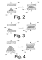
- the bonding structure can assume a variety of forms, examples of which are seen in Figures 2-4 where force F is applied to respective surfaces on wafers 102, 104 both in a 'before' illustration on the left and in an 'after' illustration on the right.
- the 'after illustration' shows the result of the compression of the bonding structure between wafers 102, 104.
- the 'after' illustration is representative of the deformation of the bonding structure, the accomplishment of a uniform and predetermined gap between opposing surfaces on wafers 102, 104, and the bonding together of wafers 102, 104.
- the 'after' illustration can be representative of the use of the deformed bonding structure to form a seal to a gas impervious chamber between wafers 102, 104.
- a weak bonding structure 108 is compressed between wafers 102, 104.
- force F is distributed over an increasingly larger surface area of opposing surfaces on wafers 102, 104 so as to effectively reduce the pressure on weak bonding structure 108.
- the material properties of weak bonding structure 108 will cause a resistance to and a cessation of further deformation such that the gap between wafers 102, 104 is set at a predetermined distance as seen in Figure 2.
- wafers 102, 104 can be heated during compression at or near a melting point of a material that is included in weak bonding structure 108.
- the temperature of wafers 102, 104 can be lowered so that weak bonding structure 108 will cease to deform via solidification of weak bonding structure 108. Additionally, force F and/or the temperature can be varied in a predetermined sequence to achieve the predetermined gap between wafers 102, 104 such that weak bonding structure 108 will cease to deform accordingly.
- Figure 3 shows 'before' and 'after' illustrations of wafers 102, 104 having a weak bonding structure 108 there between.
- the top surface of weak bonding structure 108 has a first width that is less than a second width below the top surface.
- Constant force F is applied to respective surfaces on wafers 102, 104 to compress weak bonding structure 108 between wafers 102, 104.
- force F is distributed over a first surface area at the top surface. Once the deformation reaches the second width, force F will be distributed over a largely increased surface area, resulting in a much smaller pressure upon weak bonding structure 108.
- the material properties of weak bonding structure 108 will cause a resistance to and a cessation of further deformation such that the gap between wafers 102, 104 is set at a predetermined distance as seen in Figure 3.
- wafers 102, 104 can be heated during compression at or near a melting point of a material that is included in weak bonding structure 108.
- the temperature of wafers 102, 104 can be lowered so that weak bonding structure 108 will cease to deform through the solidification thereof.
- force F and/or the temperature can be varied in a predetermined sequence to achieve the predetermined gap between wafers 102, 104 such that weak bonding structure 108 will cease to deform accordingly.
- Figure 4 illustrates a still further embodiment of the present invention where a kind of progressive step function for pressure and surface area quantities is realized during the deformation of weak bonding structure 108.
- Figures 5a-5b show, respectively, an electrical device 500 in a 'before' illustration and an electrical device 502 in an 'after' illustration that is accomplished by the compression of electrical device 500.
- Device 502 has wafers 102, 104 with a bonding structure there between that includes a bond ring 116, a bond contact 120, and a spacer contact 122.
- Each of wafers 102, 104 have a plurality of CMOS circuits 106 fabricated therein.
- Spacer contact 122 is upon wafer 104 and beneath bond contact 120 which is also upon wafer 104. Both bond ring 116 and bond contact 120 are deformed, as seen in Figure 5b, so as to bond together wafers 102, 104 in a separation of a predetermined gap.
- bond ring 116 and bond contact 120 can be designed such that, upon deformation, a gas imperious chamber (not shown) is formed. The deformation progresses until a predetermined deformation condition is reached at which the predetermined gap separates wafers 102, 104.
- the predetermined deformation condition occurs when the materials of which bond ring 116 and bond contact 120 are composed resist further deformation. Spacer contact 122 can but need not be deformed by the compression.
- An adhesion layer 114 is on wafer 102 and a diffusion barrier layer 112 is on adhesion layer 114. Diffusion barrier layer 112 prevents diffusion of materials into adhesion layer 114 and wafer 102. Adhesion layer 114 is adhered to wafer 102.
- a diffusion barrier-adhesion layer 118 upon wafer 104 and spacer contact 122 can serve one or both of the functions of preventing diffusion of materials into wafer 104 and adhering bond contact 120 to spacer contact 122.
- Spacer contact 122 is over wafer 104 and beneath diffusion barrier-adhesion layer 118.
- the material of which bond contact 120 is composed can have a melting point and/or strength that is lower than that of the material of which spacer contact 122 is composed.
- the material of which bond ring 116 is composed which can include one or more components, can have the same or a lower melting point and/or strength than that of the material of which bond contact 120 is composed.
- bond ring 116 and bond contact 120 are composed of gold or an alloy thereof, the gold interdiffuses across the interface so as to form a relatively strong bond.
- Other materials performing similarly could also be used, as well as those materials that do so in a temperature range below about 500 degrees Centigrade so that any CMOS circuitry included in wafers 102, 104 would not be damaged.
- Spacer contact 120 is generally, although not necessarily, composed of a dielectric material such as wet or dry silicon dioxide (SiO 2 ), a nitride material including silicon nitride, tetraethylorthosilicate (Si-OC 2 H 5 ) 4 ) (TEOS) based oxides, borophosphosilicate glass (BPSG), phosphosilicate glass (PSG), borosilicate glass (BSG), oxide-nitride-oxide (ONO), polyamide film, tantalum pentoxide (Ta 2 O 5 ), plasma enhanced silicon nitride (P-SiN x ), titanium oxide, oxynitride, germanium oxide, a spin on glass (SOG), any chemical vapor deposited (CVD) dielectric including a deposited oxide, a grown oxide, and /or like dielectric materials. Bond contact 120 and bond
- Figures 6a-6b show, respectively, an electrical device 600 in a 'before' illustration and an electrical device 602 in an 'after' illustration after compression of electrical device 600, each having wafers 102, 104 with a bonding structure there between that includes a bond ring 116, a bond contact 120, and a spacer contact 122.
- Spacer contact 122 is over wafer 104, underneath diffusion barrier-adhesion layer 118, and beneath bond contact 120. Both bond ring 116 and bond contact 120 are deformed to bond together wafers 102, 104 in a separation of a predetermined gap, as seen in Figure 6b.
- the resultant bonding structure can be designed so as to form a closed region, a gas impervious chamber, or a hermetically sealed region (not shown).
- the deformation of the bonding structure can progress until a predetermined deformation condition is reached.
- the predetermined deformation condition occurs when the materials of which bond ring 116 and bond contact 120 are composed resist further deformation.
- Spacer contact 122 can but need not be deformed by the compression.
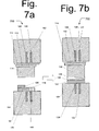
- Figures 7a-7b show, respectively, an electrical device 700 in a 'before' illustration and an electrical device 702 in an 'after' illustration after compression of electrical device 700, each having wafers 102, 104 with a bonding structure there between that includes a bond ring 116, a bond contact 120, and a spacer contact 122.
- Spacer contact 122 is upon wafer 104 and beneath diffusion barrier-adhesion layer 118 and bond contact 120.
- An alloy 126 which can be formed by diffusion or melting, such as a eutectic alloy or an intermetallic silicide alloy, is formed by bond ring 116 and bond contact 120 as bond contact 120 is deformed, whereas variation in temperature and/or pressure may also be used to form alloy 126.
- bond ring 116 can be composed of gold or a gold alloy and bond contact 120 can be gold, silicon, or a gold film stack.
- the result of the compression between wafers 102, 104, the deformation of bond contact 120, and the formation of alloy 126 is the bonding together of wafers 102, 104 in a separation of a predetermined gap, where the deformation progresses until a predetermined deformation condition is reached.
- the predetermined deformation condition occurs when alloy 126 forms and the material of which bond contact 120 is composed resists further deformation at a predetermined pressure.
- Spacer contact 122 can, but need not, be deformed by the compression.
- the process and bonding structure can be designed such that a sealed region, a gas impervious chamber, or a hermetic seal is formed at least in part by bond ring 116, alloy 126, and deformed bond contact 120.
- Electrical devices 502, 602, and 702, respectively seen in Figures 5b, 6b, and 7b, can be used in the fabrication of MEMS devices.
- a process 800 for doing so is seen in Figure 8.
- integrated circuits (ICs) are fabricated in substrates to be bonded together.
- a bonding structure which can include one or more components, is formed on one or more of the substrates that are to be bonded together.
- the bonding structure is compressed between adjacent substrates to attain a deformation condition. The attainment of the deformation condition accomplishes the formation of a bond between the substrates.
- the resulting bonding structure can be used to form a sealed region, a gas impervious chamber, or a hermetically sealed region between the bonded substrates.
- a predetermined gap or distance can exist between the bonded substrates as a result of the deformation condition. Electrical interconnections can also be made between the substrates.
- the bonded substrates are subjected to processes that include saw/dice, wire bond, and final package at step 808. Device or die testing can optionally be performed at step 810.
- this invention is also applicable to alternative bonded structure technologies, such as a die that encapsulates therein a closed environment or hermetic sealed atmosphere, and MEMS devices that can be formed by the foregoing processes including MEMS devices in air bag applications, field emitter display devices, accelerometers, bolometers, mirror arrays, optical switches, pressure gauges, memory storage devices such as atomic resolution storage devices, turbine chambers, and combustion chambers.
- the process of bonding substrates together which can include a heat treatment such as an annealing process, can be conducted at temperatures at or below approximately 450 degrees Celsius.
- An annealing chamber can be used to accomplish the bonding process.
- the bonding process may change or "ramp" the temperature. By keeping temperatures of the bonding or annealing process below approximately 450 degrees Celsius, any CMOS circuitry included in either of the bonded substrates should not be damaged.
- the substrates can be pressed together at a pressure of about zero MPa to about 300 MPa to form a bond there between.
- a bond is "sufficient" for the purposes of the present invention when it is capable of maintaining an alignment of adjacent substrates with respect to each other during normal operation of the electrical device.
- the bond should be sufficient to keep the bonded substrates attached and aligned as well as being configured to form an electrical connection between the integrated circuits in the respective substrates.
- One skilled in the art should realize that a broad variety of dimensions, materials, temperatures, times, and pressures are contemplated to accomplish the devices, structures, and processes disclosed herein, and that the embodiments of the present invention can be fabricated using a broad variety of process equipment in a semiconductor fabrication operation.
Landscapes
- Engineering & Computer Science (AREA)
- Computer Hardware Design (AREA)
- Microelectronics & Electronic Packaging (AREA)
- Micromachines (AREA)
- Combinations Of Printed Boards (AREA)
- Production Of Multi-Layered Print Wiring Board (AREA)
- Pressure Sensors (AREA)
Abstract
Description
Claims (10)
- An electrical device (100, 502, 602, 702) comprising a plurality of integrated circuits (106) respectively fabricated in a first substrate (102) bonded to a second substrate (104) by a bond (111) that deforms above, but not below, a deformation condition selected from the group consisting of:a predetermined pressure from opposing surfaces on the first and second substrates (102, 104); anda predetermined combination of temperature and pressure from opposing surfaces on the first and second substrates (102, 104).
- The electrical device (100, 502, 602, 702) as defined in Claim 1, wherein the bond further comprises a first material (120) that deforms when subjected to the deformation condition and a second material (122) that:makes contact with the opposing surfaces of the first and second substrates (102, 104); andis not deformed when subjected to the deformation condition.
- The electrical device (100, 502, 602, 702) as defined in Claim 2, wherein the first and second materials (120, 122) that, respectively, are and are not deformed when subjected to the deformation condition have material properties selected from the group consisting of:respectively lower and higher strength; andrespectively lower and higher melting point.
- An electrical device (502, 602, 702) comprising a plurality of integrated circuits (106) respectively fabricated in a first substrate (102) bonded to a second substrate (104) by a bonding structure that has a first contact structure (120 or 122) upon a second contact structure (120 or 122), wherein:each of the first and second contact structure (120, 122) makes contact with opposing surfaces on the first and second substrates (102, 104);one, but not both, of the first and second contact structures (120, 122) is deformed when subjected to by a state selected from the group consisting of:a predetermined pressure of the opposing surfaces of the first and second substrates (102, 104); anda predetermined combination of temperature and pressure of the opposing surfaces of the first and second substrates (102, 104).
- The electrical device (502, 602, 702) as defined in Claim 4, wherein one of the first and second contact structures (120, 122) comprises a material having a higher strength than that of a material comprising the other of the first and second contact structures (120, 122).
- An electrical device (502, 602, 702) comprising:wherein:a portion of a first semiconductor wafer (102) having a plurality of CMOS circuits (106) and a first surface;a portion of a second semiconductor wafer (104) having a plurality of CMOS circuits (106) and a second surface;an interface between the first and second surfaces, the interface including:a spacer contact (122) on the first surface;a bond ring (116) on the second surface;a bond contact (120) between the spacer contact (122) and the bond ring (116);the bond contact (120) has a variable thickness between the first and second surfaces;the bond contact (120) is bonded to the bond ring (116); andthe bond contact (120) is deformed when subjected to a deformation condition selected from the group consisting of:a predetermined pressure from the first and second surfaces; anda predetermined combination of temperature and pressure from the first and second surfaces;the spacer contact (122) is not deformed when subjected to the deformation condition.
- An electrical device (502, 602, 702) comprising:wherein:a portion of a first semiconductor wafer (102) having a plurality of CMOS circuits (106) and a first surface;a portion of a second semiconductor wafer (104) having a plurality of CMOS circuits (106) and a second surface;an interface between the first and second surfaces, the interface including:a spacer contact (122) on the first surface;a bond ring (116) on the second surface;a bond contact (120) in contact with the spacer contact (122) andthe bond ring (116);the bond ring (116) has a variable thickness between the first and second surfaces;the bond contact (120) has a variable thickness between the bond ring (116) and the spacer contact (122);the bond contact (120) is bonded to the bond ring (116); andthe bond contact (120) is deformed when subjected to a deformation condition selected from the group consisting of:a predetermined pressure from the first and second surfaces; anda predetermined combination of temperature and pressure from the first and second surfaces;the spacer contact (122) is not deformed when subjected to the deformation condition.
- A method of making an electrical device (100, 502, 602, 702), the method comprising:forming a bonding structure (111) on at least one of first and second substrates (102, 104) each having a plurality of integrated circuits (106) fabricated therein;compressing the bonding structure (111) between the opposing surfaces on the first and second substrates (102, 104) while applying a deformation condition to the bonding structure (111) to deform the bonding structure (111) until the bonding structure (111) bonds together the first and second substrates (102, 104), wherein the bonding structure (111) deforms above, but not below, the deformation condition which is selected from the group consisting of:a predetermined pressure of the opposing surfaces of the first and second substrates (102, 104) on the bonding structure (111); anda predetermined combination of temperature and pressure of the opposing surfaces of the first and second substrates (102, 104) on the bonding structure (111).
- A method of making an electrical device (502, 602, 702), the method comprising:wherein the spacer contact (122) is not deformed by the deformation condition.forming a bond ring (116) on a portion of a first semiconductor wafer (102) having a plurality of CMOS circuits (106) fabricated therein;forming a spacer contact (122) on a portion of a second semiconductor wafer (104) having a plurality of CMOS circuits (106) fabricated therein;forming a bond contact (120) on the spacer contact (122) and on a surface on the portion of the second semiconductor wafer (104);pressing the bond ring (116) against the bond contact (120) to deform the bond contact (120) until:the bond contact (120) is bonded to the bond ring (116); andthe portions of the first and second semiconductor wafers (104) are subjected to a deformation condition selected from the group consisting of:a predetermined pressure at an interface between the bond ring (116) and the bond contact (120); anda predetermined combination of temperature and pressure at the interface between the bond ring (116) and the bond contact (120);
- A method of making an electrical device (502, 602, 702), the method comprising:forming a bond ring (116) on a portion of a first semiconductor wafer (102) having a plurality of CMOS circuits (106) fabricated therein;forming a spacer contact (122) on a portion of a second semiconductor wafer (104) having a plurality of CMOS circuits (106) fabricated therein;forming a bond contact (120) on the spacer contact (122); andpressing the bond ring (116) against the bond contact (120) to deform the bond contact (120) until: the bond contact (120) is bonded to the bond ring (116); and
the portions of the first and second semiconductor wafers (104) are subjected to a deformation condition during which the spacer contact (122) is not deformed, the deformation condition being selected from the group consisting of:a predetermined pressure between the bond ring (116) and the bond contact (120); anda predetermined combination of temperature and pressure between the bond ring (116) and the bond contact (120).
Applications Claiming Priority (2)
| Application Number | Priority Date | Filing Date | Title |
|---|---|---|---|
| US114392 | 2002-04-01 | ||
| US10/114,392 US6969667B2 (en) | 2002-04-01 | 2002-04-01 | Electrical device and method of making |
Publications (2)
| Publication Number | Publication Date |
|---|---|
| EP1351285A2 true EP1351285A2 (en) | 2003-10-08 |
| EP1351285A3 EP1351285A3 (en) | 2006-12-27 |
Family
ID=28041043
Family Applications (1)
| Application Number | Title | Priority Date | Filing Date |
|---|---|---|---|
| EP03251979A Withdrawn EP1351285A3 (en) | 2002-04-01 | 2003-03-28 | Electrical device comprising two substrates bonded together and method of making same |
Country Status (4)
| Country | Link |
|---|---|
| US (1) | US6969667B2 (en) |
| EP (1) | EP1351285A3 (en) |
| JP (1) | JP2003309245A (en) |
| TW (1) | TWI253698B (en) |
Families Citing this family (15)
| Publication number | Priority date | Publication date | Assignee | Title |
|---|---|---|---|---|
| US20030119278A1 (en) * | 2001-12-20 | 2003-06-26 | Mckinnell James C. | Substrates bonded with oxide affinity agent and bonding method |
| US6871942B2 (en) * | 2002-04-15 | 2005-03-29 | Timothy R. Emery | Bonding structure and method of making |
| CA2485022A1 (en) * | 2002-04-15 | 2003-10-23 | Schott Ag | Method for connecting substrates and composite element |
| DE102005001449B3 (en) * | 2005-01-12 | 2006-07-20 | Fraunhofer-Gesellschaft zur Förderung der angewandten Forschung e.V. | A method for generating a predetermined internal pressure in a cavity of a semiconductor device |
| FR2890067B1 (en) * | 2005-08-30 | 2007-09-21 | Commissariat Energie Atomique | METHOD FOR SEALING OR SOLDING TWO ELEMENTS BETWEEN THEM |
| US7948034B2 (en) * | 2006-06-22 | 2011-05-24 | Suss Microtec Lithography, Gmbh | Apparatus and method for semiconductor bonding |
| US7417310B2 (en) | 2006-11-02 | 2008-08-26 | Entorian Technologies, Lp | Circuit module having force resistant construction |
| FR2935537B1 (en) * | 2008-08-28 | 2010-10-22 | Soitec Silicon On Insulator | MOLECULAR ADHESION INITIATION METHOD |
| FR2943177B1 (en) | 2009-03-12 | 2011-05-06 | Soitec Silicon On Insulator | METHOD FOR MANUFACTURING A MULTILAYER STRUCTURE WITH CIRCUIT LAYER REPORT |
| SE537499C2 (en) | 2009-04-30 | 2015-05-26 | Silex Microsystems Ab | Bonding material structure and process with bonding material structure |
| FR2947380B1 (en) | 2009-06-26 | 2012-12-14 | Soitec Silicon Insulator Technologies | METHOD OF COLLAGE BY MOLECULAR ADHESION. |
| US8378490B2 (en) | 2011-03-15 | 2013-02-19 | Taiwan Semiconductor Manufacturing Company, Ltd. | Semiconductor apparatus including a metal alloy between a first contact and a second contact |
| US8900906B2 (en) | 2012-03-08 | 2014-12-02 | Robert Bosch Gmbh | Atomic layer deposition strengthening members and method of manufacture |
| TWI476839B (en) * | 2012-07-06 | 2015-03-11 | 國立交通大學 | Wafer sub-micro bonding method and bonding layer thereof |
| US9199838B2 (en) | 2013-10-25 | 2015-12-01 | Robert Bosch Gmbh | Thermally shorted bolometer |
Family Cites Families (7)
| Publication number | Priority date | Publication date | Assignee | Title |
|---|---|---|---|---|
| JPS4831507B1 (en) * | 1969-07-10 | 1973-09-29 | ||
| US6252229B1 (en) * | 1998-07-10 | 2001-06-26 | Boeing North American, Inc. | Sealed-cavity microstructure and microbolometer and associated fabrication methods |
| JP3303791B2 (en) * | 1998-09-02 | 2002-07-22 | 株式会社村田製作所 | Electronic component manufacturing method |
| JP4420538B2 (en) * | 1999-07-23 | 2010-02-24 | アバゴ・テクノロジーズ・ワイヤレス・アイピー(シンガポール)プライベート・リミテッド | Wafer package manufacturing method |
| US6428942B1 (en) * | 1999-10-28 | 2002-08-06 | Fujitsu Limited | Multilayer circuit structure build up method |
| US6521477B1 (en) * | 2000-02-02 | 2003-02-18 | Raytheon Company | Vacuum package fabrication of integrated circuit components |
| US6853087B2 (en) * | 2000-09-19 | 2005-02-08 | Nanopierce Technologies, Inc. | Component and antennae assembly in radio frequency identification devices |
-
2002
- 2002-04-01 US US10/114,392 patent/US6969667B2/en not_active Expired - Lifetime
-
2003
- 2003-01-15 TW TW092100815A patent/TWI253698B/en not_active IP Right Cessation
- 2003-03-19 JP JP2003074764A patent/JP2003309245A/en not_active Withdrawn
- 2003-03-28 EP EP03251979A patent/EP1351285A3/en not_active Withdrawn
Also Published As
| Publication number | Publication date |
|---|---|
| TWI253698B (en) | 2006-04-21 |
| US20030183307A1 (en) | 2003-10-02 |
| US6969667B2 (en) | 2005-11-29 |
| TW200305232A (en) | 2003-10-16 |
| EP1351285A3 (en) | 2006-12-27 |
| JP2003309245A (en) | 2003-10-31 |
Similar Documents
| Publication | Publication Date | Title |
|---|---|---|
| US6969667B2 (en) | Electrical device and method of making | |
| TWI511190B (en) | Wafer-level structure and method for manufacturing and packaging micro-motor systems | |
| US8304861B2 (en) | Substrate bonding with bonding material having rare earth metal | |
| US9981841B2 (en) | MEMS integrated pressure sensor and microphone devices and methods of forming same | |
| US7750462B1 (en) | Microelectromechanical systems using thermocompression bonding | |
| US6969635B2 (en) | Methods for depositing, releasing and packaging micro-electromechanical devices on wafer substrates | |
| US7863070B2 (en) | Methods for encapsulating microelectromechanical (MEM) devices on a wafer scale | |
| US20130285175A1 (en) | Micromechanical component and method for manufacturing a micromechanical component | |
| EP2425450A2 (en) | Novel bonding process and bonded structures | |
| US6995034B2 (en) | Methods for depositing, releasing and packaging micro-electromechanical devices on wafer substrates | |
| US20040224091A1 (en) | Method for the closure of openings in a film | |
| WO2005085126A1 (en) | Hermetically sealed package for optical, electronic, opto-electronic and other devices | |
| US20050079684A1 (en) | Method of manufacturing an accelerometer | |
| Mei et al. | A robust gold-silicon eutectic wafer bonding technology for vacuum packaging | |
| Lee et al. | Wafer-level vacuum/hermetic packaging technologies for MEMS | |
| US9601457B2 (en) | Method for making an electrical connection in a blind via and electrical connection obtained | |
| Henry et al. | Wafer-level packaging of aluminum nitride RF MEMS filters | |
| Vaganov et al. | Three-dimensional bonding technologies for MEMS | |
| Neysmith et al. | Modular, device-scale, direct-chip-attach packaging for microsystems | |
| Pargfrieder et al. | 3D Packaging via Advanced-Chip-to-Wafer (AC2W) bonding enables Hybrid System-in-Package (SiP) Integration | |
| CN121405029A (en) | A bonding structure, an inertial sensor device, and a bonding method | |
| WO2002090243A3 (en) | Thick sandwich wafer for mems fabrication |
Legal Events
| Date | Code | Title | Description |
|---|---|---|---|
| PUAI | Public reference made under article 153(3) epc to a published international application that has entered the european phase |
Free format text: ORIGINAL CODE: 0009012 |
|
| AK | Designated contracting states |
Kind code of ref document: A2 Designated state(s): AT BE BG CH CY CZ DE DK EE ES FI FR GB GR HU IE IT LI LU MC NL PT RO SE SI SK TR |
|
| AX | Request for extension of the european patent |
Extension state: AL LT LV MK |
|
| PUAL | Search report despatched |
Free format text: ORIGINAL CODE: 0009013 |
|
| AK | Designated contracting states |
Kind code of ref document: A3 Designated state(s): AT BE BG CH CY CZ DE DK EE ES FI FR GB GR HU IE IT LI LU MC NL PT RO SE SI SK TR |
|
| AX | Request for extension of the european patent |
Extension state: AL LT LV MK |
|
| RIC1 | Information provided on ipc code assigned before grant |
Ipc: B81B 7/00 20060101ALI20061117BHEP Ipc: H01L 21/60 20060101AFI20030812BHEP |
|
| AKX | Designation fees paid | ||
| REG | Reference to a national code |
Ref country code: DE Ref legal event code: 8566 |
|
| STAA | Information on the status of an ep patent application or granted ep patent |
Free format text: STATUS: THE APPLICATION IS DEEMED TO BE WITHDRAWN |
|
| 18D | Application deemed to be withdrawn |
Effective date: 20070628 |