EP1351076A2 - Diffraction grating manufacturing method in an optical waveguide and the manufacturing apparatus - Google Patents
Diffraction grating manufacturing method in an optical waveguide and the manufacturing apparatus Download PDFInfo
- Publication number
- EP1351076A2 EP1351076A2 EP03004377A EP03004377A EP1351076A2 EP 1351076 A2 EP1351076 A2 EP 1351076A2 EP 03004377 A EP03004377 A EP 03004377A EP 03004377 A EP03004377 A EP 03004377A EP 1351076 A2 EP1351076 A2 EP 1351076A2
- Authority
- EP
- European Patent Office
- Prior art keywords
- refractive
- diffraction grating
- index
- change
- optical waveguide
- Prior art date
- Legal status (The legal status is an assumption and is not a legal conclusion. Google has not performed a legal analysis and makes no representation as to the accuracy of the status listed.)
- Withdrawn
Links
- 230000003287 optical effect Effects 0.000 title claims abstract description 83
- 238000004519 manufacturing process Methods 0.000 title claims abstract description 29
- 230000001939 inductive effect Effects 0.000 claims abstract description 79
- 230000001678 irradiating effect Effects 0.000 claims description 2
- 239000013307 optical fiber Substances 0.000 description 43
- 238000009826 distribution Methods 0.000 description 28
- 238000005253 cladding Methods 0.000 description 16
- 230000000052 comparative effect Effects 0.000 description 12
- YBMRDBCBODYGJE-UHFFFAOYSA-N germanium dioxide Chemical compound O=[Ge]=O YBMRDBCBODYGJE-UHFFFAOYSA-N 0.000 description 6
- VYPSYNLAJGMNEJ-UHFFFAOYSA-N Silicium dioxide Chemical compound O=[Si]=O VYPSYNLAJGMNEJ-UHFFFAOYSA-N 0.000 description 4
- 238000002834 transmittance Methods 0.000 description 4
- 238000000034 method Methods 0.000 description 3
- 206010034972 Photosensitivity reaction Diseases 0.000 description 2
- 238000004891 communication Methods 0.000 description 2
- 239000006185 dispersion Substances 0.000 description 2
- 238000012986 modification Methods 0.000 description 2
- 230000004048 modification Effects 0.000 description 2
- 230000036211 photosensitivity Effects 0.000 description 2
- 230000000644 propagated effect Effects 0.000 description 2
- 230000001902 propagating effect Effects 0.000 description 2
- 239000000654 additive Substances 0.000 description 1
- 230000015572 biosynthetic process Effects 0.000 description 1
- 230000000694 effects Effects 0.000 description 1
- 239000011521 glass Substances 0.000 description 1
- 230000000630 rising effect Effects 0.000 description 1
Images




Classifications
-
- G—PHYSICS
- G02—OPTICS
- G02B—OPTICAL ELEMENTS, SYSTEMS OR APPARATUS
- G02B6/00—Light guides; Structural details of arrangements comprising light guides and other optical elements, e.g. couplings
- G02B6/02—Optical fibres with cladding with or without a coating
- G02B6/036—Optical fibres with cladding with or without a coating core or cladding comprising multiple layers
- G02B6/03694—Multiple layers differing in properties other than the refractive index, e.g. attenuation, diffusion, stress properties
-
- G—PHYSICS
- G02—OPTICS
- G02B—OPTICAL ELEMENTS, SYSTEMS OR APPARATUS
- G02B6/00—Light guides; Structural details of arrangements comprising light guides and other optical elements, e.g. couplings
- G02B6/02—Optical fibres with cladding with or without a coating
- G02B6/02057—Optical fibres with cladding with or without a coating comprising gratings
- G02B6/02076—Refractive index modulation gratings, e.g. Bragg gratings
- G02B6/02123—Refractive index modulation gratings, e.g. Bragg gratings characterised by the method of manufacture of the grating
- G02B6/02133—Refractive index modulation gratings, e.g. Bragg gratings characterised by the method of manufacture of the grating using beam interference
- G02B6/02138—Refractive index modulation gratings, e.g. Bragg gratings characterised by the method of manufacture of the grating using beam interference based on illuminating a phase mask
-
- G—PHYSICS
- G02—OPTICS
- G02B—OPTICAL ELEMENTS, SYSTEMS OR APPARATUS
- G02B6/00—Light guides; Structural details of arrangements comprising light guides and other optical elements, e.g. couplings
- G02B6/02—Optical fibres with cladding with or without a coating
- G02B6/02057—Optical fibres with cladding with or without a coating comprising gratings
- G02B6/02076—Refractive index modulation gratings, e.g. Bragg gratings
- G02B6/02123—Refractive index modulation gratings, e.g. Bragg gratings characterised by the method of manufacture of the grating
- G02B6/02152—Refractive index modulation gratings, e.g. Bragg gratings characterised by the method of manufacture of the grating involving moving the fibre or a manufacturing element, stretching of the fibre
-
- G—PHYSICS
- G02—OPTICS
- G02B—OPTICAL ELEMENTS, SYSTEMS OR APPARATUS
- G02B6/00—Light guides; Structural details of arrangements comprising light guides and other optical elements, e.g. couplings
- G02B6/02—Optical fibres with cladding with or without a coating
- G02B6/02057—Optical fibres with cladding with or without a coating comprising gratings
- G02B6/02076—Refractive index modulation gratings, e.g. Bragg gratings
- G02B6/02114—Refractive index modulation gratings, e.g. Bragg gratings characterised by enhanced photosensitivity characteristics of the fibre, e.g. hydrogen loading, heat treatment
- G02B6/02119—Photosensitivity profiles determining the grating structure, e.g. radial or longitudinal
Definitions
- the present invention relates to a diffraction grating device in which a diffraction grating is formed through refractive index modulation along the longitudinal direction of an optical waveguide, and a method and apparatus for manufacturing such a diffraction grating device.
- a diffraction grating device is a device in which a diffraction grating is formed through refractive index modulation along the longitudinal direction of an optical waveguide (e.g. an optical fiber) .
- an optical waveguide e.g. an optical fiber
- Bragg-type ones for which the period of the refractive index modulation is relatively short and which use Bragg reflection, and long-period-type ones for which the period of the refractive index modulation is relatively long and which use phase matching between propagation modes are known.
- a Bragg-type diffraction grating device is capable of selectively reflecting light of a specific wavelength that satisfies the Bragg condition out of light propagating along the optical waveguide, and is used, for example, as a wavelength filter in an optical communication system.
- a long-period-type diffraction grating device is capable of selectively giving loss to light of a specific wavelength that satisfies a phase matching condition out of light propagating along the optical waveguide, and is used, for example, as a loss filter in an optical communication system.
- Such diffraction grating devices are manufactured as follows. First, an optical waveguide for which the optical waveguiding region is photosensitive is prepared. For example, an optical fiber having a core region comprising silica glass to which GeO 2 has been added is prepared. Silica glass to which GeO 2 has been added is photosensitive, with the refractive index rising upon being irradiated with ultraviolet light. Refractive-index-change-inducing light of a wavelength that induces such a change in refractive index is thus irradiated onto the optical waveguide via a phase grating mask or an intensity modulating mask while scanning along the longitudinal direction.
- refractive-index-change-inducing light whose intensity is spatially modulated along the longitudinal direction of the optical waveguide is irradiated, and hence refractive index modulation is formed along the longitudinal direction of the optical waveguiding region of the optical waveguide.
- a laser light source is used as the light source that outputs the refractive-index-change-inducing light.
- the light outputted from a laser light source has a Gaussian intensity distribution in the radial direction, and the beam diameter is small.
- the refractive-index-change-inducing light may not be irradiated with uniform intensity in the radial direction onto the part of the optical waveguide that is photosensitive, or the refractive-index-change-inducing light may not be irradiated with the desired intensity distribution when scanning along the longitudinal direction.
- the diffraction grating device obtained will not have the desired optical characteristics.
- a diffraction grating device in which not only the core region but also part of the cladding region is made to be photosensitive and refractive index modulation is formed over both the core region and the cladding region, or a diffraction grating device in which the grating plane of refractive index modulation formed over both the core region and the cladding region is inclined, or a diffraction grating device in which the amplitude distribution of the refractive index modulation along the longitudinal direction is made to have a prescribed functional form, the intended desired optical characteristics will not be obtained.
- the present invention was devised to resolve the problems described above; it is an object of the present invention to provide a method and apparatus that enable a diffraction grating device having desired optical characteristics to be manufactured easily.
- the present invention provides a diffraction grating device manufacturing method, in which refractive-index-change-inducing light of a wavelength that induces a change in refractive index is irradiated onto an optical waveguide, thus forming a diffraction grating through refractive index modulation along the longitudinal direction of the optical waveguide, wherein the position of irradiation of the refractive-index-change-inducing light onto the optical waveguide is swung in a direction perpendicular to the longitudinal direction of the optical waveguide.
- the present invention also provides a diffraction grating device manufacturing apparatus that irradiates refractive-index-change-inducing light of a wavelength that induces a change in refractive index onto an optical waveguide, thus forming a diffraction grating through refractive index modulation along the longitudinal direction of the optical waveguide, the diffraction grating device manufacturing apparatus comprising (1) a light source that outputs the refractive-index-change-inducing light, (2) irradiation means for irradiating the refractive-index-change-inducing light that has been outputted from the light source onto the optical waveguide, and (3) swinging means for swinging the position of irradiation of the refractive-index-change-inducing light onto the optical waveguide by the irradiation means in a direction perpendicular to the longitudinal direction of the optical waveguide.
- the present invention also provides a diffraction grating device manufactured using the diffraction grating device manufacturing method described above.
- refractive-index-change-inducing light of a wavelength that induces a change in refractive index is irradiated onto an optical waveguide, and the position of irradiation of the refractive-index-change-inducing light onto the optical waveguide is swung in a direction perpendicular to the longitudinal direction of the optical waveguide.
- a diffraction grating device manufactured in this way has a diffraction grating formed through refractive index modulation along the longitudinal direction of the optical waveguide; the refractive-index-change-inducing light is irradiated with a desired intensity distribution onto a photosensitive region of the optical waveguide in which the diffraction grating is to be formed, and hence the diffraction grating device has desired optical characteristics.
- the position of irradiation of the refractive-index-change-inducing light onto the optical waveguide prefferably to be swung with an amplitude of at least 30 ⁇ m in the direction perpendicular to the longitudinal direction of the optical waveguide.
- the position of irradiation of the refractive-index-change-inducing light onto the optical waveguide prefferably to be scanned at a scanning speed v s in the longitudinal direction of the optical waveguide, and the position of irradiation of the refractive-index-change-inducing light onto the optical waveguide to be swung at a swing speed V B, which is faster than the scanning speed v s, in the direction perpendicular to the longitudinal direction of the optical waveguide.
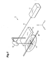
- Fig. 1 is a perspective view of a diffraction grating device manufacturing apparatus 1 according to an embodiment of the present invention.
- the diffraction grating device manufacturing apparatus 1 shown in Fig. 1 irradiates refractive-index-change-inducing light A onto an optical fiber 20, which is an optical waveguide, thus manufacturing a diffraction grating device.
- the diffraction grating device manufacturing apparatus 1 comprises a light source 11, a mirror 12, a stage 13, and a phase grating mask 14. Note that an xyz rectangular coordinate system having the z-axis parallel to the longitudinal direction of the optical fiber 20 is also shown in Fig. 1.
- the light source 11 outputs light (the refractive-index-change-inducing light A) of a wavelength that induces a change in the refractive index in a region of the optical fiber 20 that is photosensitive.
- light the refractive-index-change-inducing light A
- the light source 11 outputs the refractive-index-change-inducing light A in the z-axis direction
- the mirror 12 reflects the refractive-index-change-inducing light A, outputting the refractive-index-change-inducing light A in the x-axis direction.
- the stage 13 moves the mirror 12 in the 2-axis direction.
- the phase grating mask 14 is a flat silics glass plate having a phase grating formed on one surface thereof, and is disposed parallel to the yz-plane.
- Figs. 2A and 2B are views showing the arrangement of the phase grating mask 14 and the optical fiber 20.
- Fig. 2A is a sectional view through a plane that contains the optical axis of the optical fiber 20 and is parallel to the xz-plane
- Fig. 2B is a view from the x-axis direction (the direction in which the refractive-index-change-inducing light Ais incident on the phase grating mask 14).
- the trajectory of the position of incidence of the refractive-index-change-inducing light A onto the phase grating mask 14 is also shown in Fig. 2B.
- the optical fiber 20 comprises a core region 21 that comprises silica glass to which GeO 2 has been added and is photosensitive, and a cladding region 22 that surrounds the core region 21 and comprises silica glass.
- the phase grating mask 14 is disposed such that the surface thereof on which the phase grating is formed faces the optical fiber 20.
- the refractive-index-change-inducing lightA is incident on the phase grating mask 14
- diffracted light of the order +1 and diffracted light of order -1 are generated from the refractive-index-change-inducing light A through the diffraction effect of the phase grating, and the diffracted light of order +1 and the diffracted light of order -1 interfere with one another, whereby interference fringes are formed along the longitudinal direction in the core region 21 of the optical fiber 20.
- interference fringes refractive index modulation is formed along the longitudinal direction in the photosensitive core region 21 of the optical fiber 20.
- the position of incidence of the refractive-index-change-inducing light A onto the phase grating mask 14 is moved so as to trace out the zigzag trajectory shown in Fig. 2B. That is, the position of the irradiation of the refractive-index-change-inducing light Aonto the optical fiber 20 is scanned in the z-axis direction, and at the same time is swung in the y-axis direction.
- the scanning of the irradiation position in the z-axis direction is carried out by moving the mirror 12 using the stage 13 (scanning means) .
- the swinging of the irradiation position in the y-axis direction may be carried out, for example, by making the orientation of the reflecting surface of the mirror 12 oscillate, or by moving the optical fiber 20 and the phase grating mask 14 as a single body using a stage (not shown) that is provided separately to the stage 13 in the y-axis direction (irradiation means).
- the swinging in the y-axis direction of the position of irradiation of the refractive-index-change-inducing light A is carried out such that the whole width of the photosensitive core region 21 of the optical fiber 20 falls within the range of the swinging movement.
- the amplitude of the swing in the y-axis direction of the position of irradiation of the refractive-index-change-inducing light A is at least 30 ⁇ m. If the amplitude of the swing is at least 30 ⁇ m, then the refractive-index-change-inducing light A is irradiated uniformly in the radial direction onto the core region 21 of the optical fiber 20.
- the whole width of the photosensitive core region 21 of the optical fiber 20 falls within the range of the swing in the y-axis direction of the position of irradiation of the refractive-index-change-inducing light A at each point during the scanning, and hence the refractive-index-change-inducing light is irradiated with the desired intensity distribution along the z-axis direction of the core region 21.
- the swing speed V B is preferable for the swing speed V B to be faster than the scanning speed v s .
- the distribution of the irradiation of the refractive-index-change-inducing light A in the radial direction of the core region 21 becomes yet more uniform, and moreover the distribution of the irradiation of the refractive-index-change-inducing light A along the z-axis direction of the core region 21 becomes yet closer to the desired distribution.
- Fig. 3 is an explanatory view of a diffraction grating device 30 manufactured through the diffraction grating device manufacturing method according to the present embodiment, using the diffraction grating device manufacturing apparatus 1 according to the present embodiment.
- Fig. 3 shows a section of the diffraction grating device 30 through a plane containing the optical axis.
- the diffraction grating device 30 has a diffraction grating 23 formed therein through refractive index modulation over a certain range along the longitudinal direction of the core region 21 of the optical fiber 20 described above.
- the diffraction grating device 30 selectively reflects light of a specific wavelength that satisfies the Bragg condition in the diffraction grating 23 out of light that has propagated along the core region 21 and reached the diffraction grating 23, causing this reflected light to propagate back in the opposite direction, and transmitting light of the other wavelengths.
- the formation of the refractive index modulation is uniform in the radial direction, and moreover the amplitude distribution of the refractive index modulation along the longitudinal direction is the desired distribution, and hence the diffraction grating device 30 has the desired optical characteristics (reflection characteristics, wavelength dispersion characteristics).
- Fig. 4 is a graph showing the intensity distribution in the y-axis direction of the refractive-index-change-inducing light irradiated onto an optical fiber.
- This graph shows the intensity distribution in the y-axis direction of the refractive-index-change-inducing light for the case that the refractive-index-change-inducing light was condensed using a cylindrical lens and then irradiated onto the optical fiber via a phase grating mask.
- the intensity distribution in the y-axis direction of the refractive-index-change-inducing light irradiated onto the optical fiber is Gaussian.
- refractive-index-change-inducing light having such an intensity distribution in the y-axis direction is irradiated onto an optical fiber.
- a diffraction grating device of Example 1 was formed in an optical fiber having a core region and a cladding region as shown in Fig. 3.
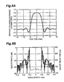
- Figs. 5A and 5B are graphs showing various characteristics of the diffraction grating device of Example 1
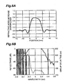
- Figs. 6A and 6B are graphs showing various characteristics of the diffraction grating device of a Comparative Example 1.
- Figs. 5A and 6A show the amplitude distribution of the refractive index modulation along the longitudinal direction
- Figs. 5B and 6B show the wavelength dependence of each of the reflectance and the group delay time.
- the amplitude distribution of the refractive index modulation along the longitudinal direction has been made to have a prescribed functional form (Fig. 5A), and the group delay time has been made to be approximately constant (i.e. the absolute value of the wavelength dispersion has been made to be low) within the reflection zone (Fig. 5B)
- the diffraction grating device of Example 1 was manufactured through the manufacturing method described above in which the position of irradiation of the refractive-index-change-inducing light onto the optical fiber is swung in the y-axis direction, and hence the desired characteristics were obtained.
- a diffraction grating device of Example 2 was also formed in an optical fiber having a core region and a cladding region as shown in Fig. 3.
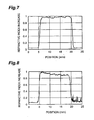
- Fig. 7 is a graph showing the amplitude distribution of the refractive index modulation along the longitudinal direction of the diffraction grating device of Example 2
- Fig. 8 is a graph showing the amplitude distribution of the refractive index modulation along the longitudinal direction of a diffraction grating device of a Comparative Example 2.
- the diffraction grating devices of Example 2 and Comparative Example 2 were each manufactured with the intention that the amplitude of the refractive index modulation along the longitudinal direction would be constant.
- the diffraction grating device of Example 2 was manufactured through the manufacturing method described above in which the position of irradiation of the refractive-index-change-inducing light onto the optical fiber is swung in the y-axis direction, and hence the desired refractive index modulation amplitude was obtained (Fig. 7).
- the diffraction grating device of Comparative Example 2 was manufactured without swinging the position of irradiation of the refractive-index-change-inducing light in the y-axis direction, andhence the desired refractive index modulation amplitude was not obtained (Fig. 8).
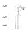
- FIG. 9A shows a section of the optical fiber 40 through a plane perpendicular to the optical axis
- Fig. 9B shows the refractive index distribution in the radial direction for the optical fiber 40
- Fig. 9C shows the photosensitivity distribution in the radial direction for the optical fiber 40.
- Fig. 10 is an explanatory view of the diffraction grating device 50 of Example 3, and shows a section through a plane containing the optical axis.
- the optical fiber 40 comprises, in order from the optical axis outwards, an inner core region 41, an outer core region 42, an inner cladding region 43, and an outer cladding region 44 (Fig. 9A) .
- Prescribed additives (Ge, B, etc.) are contained in each of the regions, and the refractive index of each of the inner core region 41 and the outer core region 42 is set to be higher than the refractive index of each of the inner cladding region 43 and the outer cladding region 44 (Fig. 9B) .
- the photosensitivity is made to be highest in the inner cladding region 43, andnext highest in the outer core region 42 (Fig. 9C) .
- the outside diameter of the inner cladding region 43 is approximately 20 ⁇ m.
- the diffraction grating device 50 of Example 3 has a diffraction grating 45 formed therein through refractive index modulation over both the outer core region 42 and the inner cladding region 43 in a certain range along the longitudinal direction of the optical fiber 40, and the grating plane of the diffraction grating 45 is inclined (Fig. 10), i.e. the grating plane of the diffraction grating 45 and the optical axis of the optical fiber 4 0 are not orthogonal to one another.
- Such a diffraction grating device 50 selectively reflects light of a specific wavelength that satisfies the Bragg condition in the diffraction grating 45 out of light that has propagated along the core region (the inner core region 41 and the outer core region 42) and reached the diffraction grating 45, causing most of this reflected light to radiate into the cladding region (the inner cladding region 43 and the outer cladding region 44), and transmitting light of other wavelengths.
- Fig. 11 is a graph showing the wavelength dependence of each of the transmittance and the reflectance for the diffraction grating device of Example 3
- Fig. 12 is a graph showing the wavelength dependence of each of the transmittance and the reflectance for the diffraction grating device of a Comparative Example 3.
- the diffraction grating device of Example 3 was manufactured through the method described above in which the position of irradiation of the refractive-index-change-inducing light onto the optical fiber is swung in the y-axis direction, and hence the refractive-index-change-inducing light is irradiated uniformly in the radial direction, and thus the reflectance is kept low as desired (Fig. 11) .
- the diffraction grating device of Comparative Example 3 was manufactured without swinging the position of irradiation of the refractive-index-change-inducing light in the y-axis direction, and hence the refractive-index-change-inducing light was irradiated mainly onto the outer core region 42, and thus the reflectance became high (Fig. 12).
- the swinging means for swinging the position of irradiation of the refractive-index-change-inducing light onto the optical fiber in a direction perpendicular to the longitudinal direction of the optical fiber (the y-axis direction) may have another form.
- the swinging means may have the constitution shown in Figs. 13A and 13B.
- Fig. 13A is a view from the y-axis direction
- Fig. 13B is a view from the x-axis direction.
- the refractive-index-change-inducing lightAoutputted from the light source 11 initiallyproceeds in the y-axis direction is then reflected by a mirror 15 and proceeds in the z-axis direction, and is then reflected by the mirror 12, proceeds in the x-axis direction, and is incident on the phase grating mask 14.
- the mirror 15 can be swung in the y-axis direction. Through the swing of the mirror 15 in the y-axis direction, the position of irradiation of the refractive-index-change-inducing light A onto the optical fiber 20 is swung in the y-axis direction.
- the swinging means may be constituted as shown in Figs. 14A and 14B.
- Fig. 14A is a view from the y-axis direction
- Fig. 14B is a view from the z-axis direction.
- a cylindrical lens 16 is provided between the mirror 12 and the phase grating mask 14.
- the cylindrical lens 16 can be swung in the y-axis direction.
- the position of irradiation of the refractive-index-change-inducing light A onto the optical fiber 20 is moved back-and-forth in the y-axis direction.
- a diffraction grating 23 or 45 is formed in a optical fiber 20 or 40 as the diffraction grating device 1; however, there is no limitation to this, but rather the present invention can also be applied to the case of forming a diffraction grating in a planar waveguide as the optical waveguide.
- refractive-index-change-inducing light of a wavelength that induces a change in refractive index is irradiated onto an optical waveguide, and the position of irradiation of the refractive-index-change-inducing light onto the optical waveguide is swung in a direction perpendicular to the longitudinal direction of the optical waveguide.
- Adiffraction grating device manufactured in this way will have desired optical characteristics, since the refractive-index-change-inducing light is irradiated with the desired intensity distribution onto the photosensitive region of the optical waveguide in which the diffraction grating is to be formed.
Landscapes
- Physics & Mathematics (AREA)
- General Physics & Mathematics (AREA)
- Optics & Photonics (AREA)
- Engineering & Computer Science (AREA)
- Manufacturing & Machinery (AREA)
- Diffracting Gratings Or Hologram Optical Elements (AREA)
- Optical Fibers, Optical Fiber Cores, And Optical Fiber Bundles (AREA)
- Optical Integrated Circuits (AREA)
Abstract
Description
Claims (7)
- A diffraction grating device manufacturing method, in which refractive-index-change-inducing light of a wavelength that induces a change in refractive index is irradiated onto an optical waveguide, thus forming a diffraction grating through refractive index modulation along the longitudinal direction of said optical waveguide;
wherein the position of irradiation of said refractive-index-change-inducing light onto said optical waveguide is swung in a direction perpendicular to the longitudinal direction of said optical waveguide. - The diffraction grating device manufacturing method according to claim 1, wherein the position of irradiation of said refractive-index-change-inducing light onto said optical waveguide is swung with an amplitude of at least 30µm in the direction perpendicular to the longitudinal direction of said optical waveguide.
- The diffraction grating device manufacturing method according to claim 1, wherein the position of irradiation of said refractive-index-change-inducing light onto said optical waveguide is scanned at a scanning speed vs in the longitudinal direction of said optical waveguide, and the position of irradiation of said refractive-index-change-inducing light onto said optical waveguide is swung at a swing speed VB, which is faster than said scanning speed vS, in the direction perpendicular to the longitudinal direction of said optical waveguide.
- A diffraction grating device manufacturing apparatus that irradiates refractive-index-change-inducing light of a wavelength that induces a change in refractive index onto an optical waveguide, thus forming a diffraction grating through refractive index modulation along the longitudinal direction of said optical waveguide, the diffraction grating device manufacturing apparatus comprising:a light source that outputs said refractive-index-change-inducing light;irradiation means for irradiating said refractive-index-change-inducing light that has been outputted from said light source onto said optical waveguide; andswinging means for swinging the position of irradiation of said refractive-index-change-inducing light onto said optical waveguide by said irradiation means in a direction perpendicular to the longitudinal direction of said optical waveguide.
- The diffraction grating device manufacturing apparatus according to claim 4, wherein said swinging means swings the position of irradiation of said refractive-index-change-inducing light onto said optical waveguide with an amplitude of at least 30µm in the direction perpendicular to the longitudinal direction of said optical waveguide.
- The diffraction grating device manufacturing apparatus according to claim 4, further comprising:wherein said swinging means swings the position of irradiation of said refractive-index-change-inducing light at a swing speed VB that is faster than the scanning speed vs of the scanning by said scanning means.scanning means for scanning the position of irradiation of said refractive-index-change-inducing light onto said optical waveguide by said irradiation means in the longitudinal direction of said optical waveguide;
- A diffraction grating device, manufactured using the diffraction grating device manufacturing method according to claim 1.
Applications Claiming Priority (2)
| Application Number | Priority Date | Filing Date | Title |
|---|---|---|---|
| JP2002057646A JP2003255159A (en) | 2002-03-04 | 2002-03-04 | Optical waveguide type diffraction grating element manufacturing method, optical waveguide type diffraction grating element manufacturing apparatus, and optical waveguide type diffraction grating element |
| JP2002057646 | 2002-03-04 |
Publications (2)
| Publication Number | Publication Date |
|---|---|
| EP1351076A2 true EP1351076A2 (en) | 2003-10-08 |
| EP1351076A3 EP1351076A3 (en) | 2005-01-26 |
Family
ID=27800127
Family Applications (1)
| Application Number | Title | Priority Date | Filing Date |
|---|---|---|---|
| EP03004377A Withdrawn EP1351076A3 (en) | 2002-03-04 | 2003-03-03 | Diffraction grating manufacturing method in an optical waveguide and the manufacturing apparatus |
Country Status (3)
| Country | Link |
|---|---|
| US (1) | US6804437B2 (en) |
| EP (1) | EP1351076A3 (en) |
| JP (1) | JP2003255159A (en) |
Families Citing this family (3)
| Publication number | Priority date | Publication date | Assignee | Title |
|---|---|---|---|---|
| JP4222141B2 (en) * | 2003-07-25 | 2009-02-12 | 沖電気工業株式会社 | Manufacturing method and manufacturing apparatus for superstructure fiber Bragg grating |
| WO2017073670A1 (en) * | 2015-10-27 | 2017-05-04 | 住友電気工業株式会社 | Optical fiber and slanted fiber grating including same |
| JP6879300B2 (en) * | 2016-05-12 | 2021-06-02 | 住友電気工業株式会社 | Manufacturing methods for multi-core optical fibers, fiber bragg gratings and fiber bragg gratings |
Family Cites Families (7)
| Publication number | Priority date | Publication date | Assignee | Title |
|---|---|---|---|---|
| US5559907A (en) * | 1994-02-17 | 1996-09-24 | Lucent Technologies Inc. | Method of controlling polarization properties of a photo-induced device in an optical waveguide and method of investigating structure of an optical waveguide |
| JP3427961B2 (en) | 1996-07-30 | 2003-07-22 | 日本電信電話株式会社 | Method and apparatus for producing fiber grating |
| JP3401419B2 (en) | 1997-11-12 | 2003-04-28 | 沖電気工業株式会社 | Optical filter alignment device and optical filter alignment method |
| JP3401420B2 (en) * | 1997-11-12 | 2003-04-28 | 沖電気工業株式会社 | Optical filter alignment device and optical filter alignment method |
| EP1345050A4 (en) * | 2000-11-28 | 2005-10-12 | Fujikura Ltd | Method and device for manufacturing optical fiber grating, optical fiber grating, optical module, and optical communication system |
| JP3813059B2 (en) * | 2000-12-26 | 2006-08-23 | 三菱電機株式会社 | Grating production method |
| US6766080B2 (en) * | 2001-07-10 | 2004-07-20 | Sumitomo Electric Industries, Ltd. | Optical waveguide type defraction grating device and a method of manufacturing thereof |
-
2002
- 2002-03-04 JP JP2002057646A patent/JP2003255159A/en active Pending
-
2003
- 2003-03-03 EP EP03004377A patent/EP1351076A3/en not_active Withdrawn
- 2003-03-04 US US10/377,665 patent/US6804437B2/en not_active Expired - Fee Related
Also Published As
| Publication number | Publication date |
|---|---|
| JP2003255159A (en) | 2003-09-10 |
| US6804437B2 (en) | 2004-10-12 |
| US20030165294A1 (en) | 2003-09-04 |
| EP1351076A3 (en) | 2005-01-26 |
Similar Documents
| Publication | Publication Date | Title |
|---|---|---|
| CA2087511C (en) | Method of fabricating bragg gratings using a silica glass phase grating mask | |
| USRE39865E1 (en) | Method of fabricating Bragg gratings using a silica glass phase grating mask and mask used by same | |
| US5636304A (en) | Article comprising a spatially varying Bragg grating in an optical fiber | |
| JP2931194B2 (en) | Method of forming a distributed Bragg reflector in an optical medium | |
| US5604829A (en) | Optical waveguide with diffraction grating and method of forming the same | |
| RU2193220C2 (en) | Amplitude mask, device and process of manufacture of filter based on large-period lattice using such amplitude mask | |
| EP0000810A1 (en) | Method of and apparatus for forming focusing diffraction gratings for integrated optics | |
| JPH09508713A (en) | Light grating | |
| US5625472A (en) | Method for forming distributed Bragg reflectors in optical media | |
| EP0881515B1 (en) | Spatial filter for high power laser beam | |
| JP2003505714A (en) | How to write grating structure | |
| US5848207A (en) | Optical device formed with grating therein, add/drop filter using same, and method of fabricating same | |
| RU2001107252A (en) | DEVICE FOR MANUFACTURE OF FIBER OPTICAL FIBER LATTICES WITH A LARGE PERIOD, AND ALSO BASED ON ITS DEVICE FOR MANUFACTURE OF TWO-BAND FIBER OPTIC LATTICES WITH A LARGE PERIOD | |
| EP1121613A1 (en) | Apparatus for manufacturing long-period fiber gratings and apparatus for manufacturing two-band long-period fiber gratings using the same | |
| US5953471A (en) | Optical communication system having short period reflective Bragg gratings | |
| CN112764153B (en) | Band-stop filter suitable for any spectral shape, and preparation method and system thereof | |
| US6804437B2 (en) | Diffraction grating device manufacturing method, diffraction grating device manufacturing apparatus, and diffraction grating device | |
| TW569041B (en) | Reflection-grid optical waveguide-path type and its production method | |
| US7079729B2 (en) | Apparatus for generating an optical interference pattern | |
| JPH08286009A (en) | Chirp grid forming device | |
| JPH07261038A (en) | Optical waveguide and optical transmission system | |
| JPH08286061A (en) | Optical filter | |
| EP1207410A1 (en) | Method and equipment for writing a bragg grating in a waveguide | |
| KR101753898B1 (en) | Apparatus for excitation of surface plasmon wave | |
| JPH11295541A (en) | Waveguide type diffraction grating manufacturing method and waveguide type diffraction grating manufacturing apparatus |
Legal Events
| Date | Code | Title | Description |
|---|---|---|---|
| PUAI | Public reference made under article 153(3) epc to a published international application that has entered the european phase |
Free format text: ORIGINAL CODE: 0009012 |
|
| AK | Designated contracting states |
Kind code of ref document: A2 Designated state(s): AT BE BG CH CY CZ DE DK EE ES FI FR GB GR HU IE IT LI LU MC NL PT RO SE SI SK TR |
|
| AX | Request for extension of the european patent |
Extension state: AL LT LV MK |
|
| RTI1 | Title (correction) |
Free format text: DIFFRACTION GRATING MANUFACTURING METHOD IN AN OPTICAL WAVEGUIDE AND THE MANUFACTURING APPARATUS |
|
| PUAL | Search report despatched |
Free format text: ORIGINAL CODE: 0009013 |
|
| AK | Designated contracting states |
Kind code of ref document: A3 Designated state(s): AT BE BG CH CY CZ DE DK EE ES FI FR GB GR HU IE IT LI LU MC NL PT RO SE SI SK TR |
|
| AX | Request for extension of the european patent |
Extension state: AL LT LV MK |
|
| RIC1 | Information provided on ipc code assigned before grant |
Ipc: 7G 02B 6/16 A |
|
| 17P | Request for examination filed |
Effective date: 20050408 |
|
| 17Q | First examination report despatched |
Effective date: 20050511 |
|
| AKX | Designation fees paid |
Designated state(s): FR IT |
|
| REG | Reference to a national code |
Ref country code: DE Ref legal event code: 8566 |
|
| STAA | Information on the status of an ep patent application or granted ep patent |
Free format text: STATUS: THE APPLICATION IS DEEMED TO BE WITHDRAWN |
|
| 18D | Application deemed to be withdrawn |
Effective date: 20061013 |