EP1351065A1 - A field programmable device - Google Patents
A field programmable device Download PDFInfo
- Publication number
- EP1351065A1 EP1351065A1 EP02252426A EP02252426A EP1351065A1 EP 1351065 A1 EP1351065 A1 EP 1351065A1 EP 02252426 A EP02252426 A EP 02252426A EP 02252426 A EP02252426 A EP 02252426A EP 1351065 A1 EP1351065 A1 EP 1351065A1
- Authority
- EP
- European Patent Office
- Prior art keywords
- configuration
- output
- error
- input
- data
- Prior art date
- Legal status (The legal status is an assumption and is not a legal conclusion. Google has not performed a legal analysis and makes no representation as to the accuracy of the status listed.)
- Granted
Links
- 238000001514 detection method Methods 0.000 claims abstract description 28
- 239000011159 matrix material Substances 0.000 description 39
- 238000012360 testing method Methods 0.000 description 32
- 238000012545 processing Methods 0.000 description 13
- 238000000034 method Methods 0.000 description 10
- 238000013461 design Methods 0.000 description 8
- 238000012795 verification Methods 0.000 description 6
- 230000009471 action Effects 0.000 description 4
- 238000003491 array Methods 0.000 description 4
- 230000001419 dependent effect Effects 0.000 description 4
- 239000013598 vector Substances 0.000 description 3
- 238000010586 diagram Methods 0.000 description 2
- 230000006870 function Effects 0.000 description 2
- 238000012544 monitoring process Methods 0.000 description 2
- 230000008569 process Effects 0.000 description 2
- 230000003139 buffering effect Effects 0.000 description 1
- 125000004122 cyclic group Chemical group 0.000 description 1
- 230000000694 effects Effects 0.000 description 1
- 238000002438 flame photometric detection Methods 0.000 description 1
- 238000001310 location test Methods 0.000 description 1
- 230000037361 pathway Effects 0.000 description 1
- 239000007787 solid Substances 0.000 description 1
- 238000010998 test method Methods 0.000 description 1
Images




Classifications
-
- G—PHYSICS
- G01—MEASURING; TESTING
- G01R—MEASURING ELECTRIC VARIABLES; MEASURING MAGNETIC VARIABLES
- G01R31/00—Arrangements for testing electric properties; Arrangements for locating electric faults; Arrangements for electrical testing characterised by what is being tested not provided for elsewhere
- G01R31/28—Testing of electronic circuits, e.g. by signal tracer
- G01R31/317—Testing of digital circuits
- G01R31/3181—Functional testing
- G01R31/3185—Reconfiguring for testing, e.g. LSSD, partitioning
- G01R31/318516—Test of programmable logic devices [PLDs]
- G01R31/318519—Test of field programmable gate arrays [FPGA]
-
- G—PHYSICS
- G01—MEASURING; TESTING
- G01R—MEASURING ELECTRIC VARIABLES; MEASURING MAGNETIC VARIABLES
- G01R31/00—Arrangements for testing electric properties; Arrangements for locating electric faults; Arrangements for electrical testing characterised by what is being tested not provided for elsewhere
- G01R31/28—Testing of electronic circuits, e.g. by signal tracer
- G01R31/317—Testing of digital circuits
- G01R31/3181—Functional testing
- G01R31/3185—Reconfiguring for testing, e.g. LSSD, partitioning
- G01R31/318516—Test of programmable logic devices [PLDs]
-
- H—ELECTRICITY
- H03—ELECTRONIC CIRCUITRY
- H03K—PULSE TECHNIQUE
- H03K19/00—Logic circuits, i.e. having at least two inputs acting on one output; Inverting circuits
- H03K19/02—Logic circuits, i.e. having at least two inputs acting on one output; Inverting circuits using specified components
- H03K19/173—Logic circuits, i.e. having at least two inputs acting on one output; Inverting circuits using specified components using elementary logic circuits as components
- H03K19/177—Logic circuits, i.e. having at least two inputs acting on one output; Inverting circuits using specified components using elementary logic circuits as components arranged in matrix form
- H03K19/17748—Structural details of configuration resources
- H03K19/17764—Structural details of configuration resources for reliability
Definitions
- the present invention relates to a field programmable device (FPD) and in particular but not exclusively to Field Programmable Gate Arrays (FPGA).
- FPD field programmable device
- FPGA Field Programmable Gate Arrays
- PGA Programmable gate arrays
- field programmable devices FPD
- FPGA field programmable gate arrays
- a field programmable device such as the FPGA is at its most basic level a series of configurable logic blocks (CLB), interconnected by a series of configurable connections or links, and read from and written to by a configurable input/output device.
- CLB configurable logic blocks
- the effectiveness of a field programmable device is the ability of the device to represent a required digital design, and be capable of being altered without the need for complete replacement. This ability is dependent on several factors such as device speed, and the complexity of design capable of being simulated.
- the complexity of the design is itself dependent on the complexity of the interconnections between the configurable logic blocks, and the number of the configurable logic blocks. The greater the number of blocks and the more complex the interconnection environment, the more complex the design that can be realised.
- Interconnects are generally programmed, in the case of memory based FPDs by a series of switching matrices controlled by memory latches.
- the memory latches create closed or open circuits between pairs of conducting lines.
- These configuration latches are supplied configuration data from a series of configuration registers and are enabled by an address register in a manner similar to the addressing and writing to a typical memory cell.
- the address and configuration data are passed to the configuration latches by a series of configuration and address lines.
- a verification step is typically introduced after configuration and prior to using the device in an active mode.
- This verification step involves using a series of test input signals, or test vectors, and monitoring the output of the FPD.
- the output of the simulated circuit is checked against the test vector input to enable the verification step to determine if a configuration error has occurred and if enough test vectors are entered, the verification step may determine which region or which configuration latch has failed.
- This verification step therefore increases the time spent in the configuration mode. Also should any errors be detected the device has to restart the whole configuration cycle again.
- a field programmable device comprising: a plurality of logic blocks; a plurality of connections connecting said blocks; configuration means for outputting configuration data for programming said device, said configuration means providing at least one pair of outputs; and error detection means for comparing said outputs to determine if there has been a configuration error.
- the device may further comprise said error detecting means comprising means for comparing said outputs.
- the device may further comprise said comparing means comprising an XNOR gate.
- the device may further comprise said error detection means being arranged to determine the presence of an error if a pair of outputs are determined to be the same.
- the device may further comprise said error detection means comprising at least one transistor arranged to provide a predetermined output when an error is determined.
- the device may further comprise said at least one transistor comprising a pull up transistor.
- the device may further comprise at least one pair of outputs comprising a signal and its inverse.
- the device may further comprise said error detection means being arranged to determine errors in a first part of said device and then to determine errors on a second part of said device.
- the device may further comprise said error detection means being arranged to determine errors in the first part when a clock signal has a first state and to determine errors in the second part when the clock signal has a second state.
- the device may further comprise one of said first and second parts of said device comprising the outputs of said configuration means.
- the device may further comprise one of said first and second parts of said device comprising said plurality of connections.
- the device may further comprise at least one of said logic blocks and said connection means being configurable.
- the device may further comprise said error detection means being arranged to determine the location of an error.
- the device may further comprise error means comprising means for providing an output for each line of said device.
- the device may further comprise said means for providing an output for each line comprising storage means.
- the device may further comprise said means for providing an output for each line comprising said comparing means.
- Embodiments of the present invention allow the testing of configuration data to be carried out at the same time as the act of configuring the device.
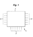
- the Field Programmable Device (FPD) 1 comprises a digital logic device 7, and a series of pins providing connections to and from the logic device, these are bi-directional and/or single directional and may be defined in each specific designed use.
- pins 3 provide digital signals to the logic device, i.e. are inputs and pins 5 provide digital signals from the logic device, i.e. are outputs.
- the FPD may be capable of being operated in one of two modes.
- the first is an active mode, whereby the device simulates the action or actions of a digital or a series of digital circuits.
- the device may receive inputs via the input pins 3 and outputs via the output pins 5, whereby these inputs may provide digital data and/or may be a clock signal.
- the second mode is a configuration mode.
- the logic device is configured dependent on input data.
- the logic device is arranged to simulate the action of the required digital circuit or circuits.
- This configuration input data may be passed to the logic device via the input pins 3 or output pins (acting as input pins) 5 or by a separate series of configuration pins 2.
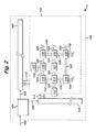
- the logic device 7 comprises a processing block 110 which comprises the elements needed to allow the FPD to simulate the required circuit.
- a series of a series of Input/Output Blocks (IOB) 117 are provided at the edges of the processing block 110.
- IOBs 117 are configurable to be capable of buffering signals received from and output to the FPD connection pins 3,5.
- the IOBs 117 are connected to the rest of the processing block 110 by a plurality of vertical conductive paths (or vertical data lines) 119, and horizontal paths (or horizontal data lines) 123. These conductive paths run in vertical 119 and horizontal 123 directions and span the processing area 110 of the digital logic device 7.
- Switching Matrices which at the intersection of vertical and horizontal paths, 119 and 123, create short or open circuits, connecting or isolating the paths, 119 and 123, in dependence of the configuration of the switching matrix.
- the switching matrix 115 thus allows a vertical path 119 to be connected to a horizontal path 123, allows a horizontal path 123 to pass through the switch matrix 115, and/or allows a vertical path 119 to pass through the switch matrix.
- CLB Configurable Logic Blocks
- the arrangement of the Configurable Logic Blocks 121 and switched matrices 115 is normally such that no two CLBs are directly connected together by a single conductive path 119,123. Therefore signals from one CLB 121 to another CLB 121 are routed via switched matrices 115.
- An alternate arrangement in some areas of the processing block allows direct connections between CLBs in some circumstances.
- the CLB 121 can be considered to comprise a series of look up tables outputting values in dependence on a series of inputs, coupled to a second stage where the values or these look up tables are logically combined or selected in dependence on the configuration of that block.
- the circuitry of the configuration block comprises a configuration controller 101, a configuration data register 125 and address register 103.
- the configuration controller 101 controls the configuration within the FPD.
- the configuration controller 101 receives signals 5 via the configuration pins 2.
- the controller 101 can instruct the address registers 103 and configuration data registers 125 via an address register conductive path 107 and a configuration register conductive path 109 respectively.
- Configuration data, as well as instructions from the controller 101 can also be loaded onto the configuration data register 125 via the same configuration register conductive path 109.
- the configuration data is stored on the configuration data register 125 and output to the elements in the processing block 110 on a series of configuration data lines 111.
- the data is directed to the correct part of the processing block in dependence on the signals output from the address register 103 via the address lines 113.
- These address lines 113 and configuration data lines 111 intersect the processing block 110, spanning all of the configurable elements in the processing block 110 (this is not shown for clarity purposes).
- FIG. 3 shows in more detail a part 130 of the processing block 110.
- Configurable Logic Blocks 121 are connected to each other via horizontal 123 and vertical 119 conductive paths. Connecting paths together and routing pathways on these conductive paths, 119 and 123, are the switching matrices 115.
- the switching matrices 115 are also connected to the configuration data lines 111 and the address lines 113, which run continuously across the processing block 110.
- FIG. 4 shows in further detail the circuitry used to configure the switch matrix 115.
- a switch matrix 115 comprises a plurality of horizontal data lines 123, a plurality of vertical data lines 119, a plurality of configuration data lines 425, a plurality of address lines 113, a plurality of enable signal generators 419, a plurality of configuration latches 427, a plurality of connecting transistors 450 and a plurality of output switch transistors 435.
- the horizontal data lines 123 pass through the switch matrix 115 from one horizontal side to the opposite side (of which one 123a is shown in figure 4).
- the vertical data lines 119 pass through the switch matrix 115 from one vertical side to the opposite vertical side (of which one 119a is shown in figure 4).
- the switch matrix configuration data lines 425 pass through the switch matrix 115, entering on one side and being connected to the configuration data lines 111, and connected on the opposite side to a series of switch matrix configuration outputs 439.
- the address lines 113 enter the switch matrix 115, and pass along the switch matrix 115.
- the lines may in some embodiments of the present invention pass through the switch matrix and exit on the opposite side to continue the path of the address lines 113 or with reference to figure 3 and figure 4 the address lines terminate within the switch matrix, with a path external to the switch matrix connecting to each of the switch matrices 115.
- the enable signal generator 419 has a first input connected to the clock signal line 401, a second input connected to an address signal 113, a first output connected to an input enable line 421 and a second output connected to an output enable line 423.
- the configuration latch 427 has a first (data) input 429 connected to the switch matrix configuration data line 425, a second (enable) input 431 connected to the input enable line 421, and an output 433.
- connection transistor 450 has its gate 451 connected to the configuration latch output 433, one of its remaining terminals 453 connected to one of the vertical data lines 119a and the remaining terminal 455 connected to one of the horizontal data lines.
- the output switch 435 has its gate connected to the output enable line 423, one of the remaining terminals connected to the output of the configuration latch, which has its enable input 431 connected to the input enable line 421 provided from the same enable signal generator 419 supplying the output enable line 423 connected to the gate of the output switch.
- the remaining terminal is connected to the switch matrix configuration data line 425 which is connected to the data input 429 of the configuration latch 427 of which the output 433 is connected to the other terminal.
- the switched matrix 115 has an array of configuration latches.
- Each element 461 of this array comprises a pair of enable lines, input enable 421 and output enable 423, switch matrix configuration data line 439 running horizontally through the element, a configuration latch 427 with the enable input connected to the input enable 421, and the data input 429 connected to the switch matrix configuration data line 425.
- the output of the configuration latch 427 is passed to the output switch 435 which can pass the output back to the configuration line 425.
- the configuration latch output 433 is also passed to a connection switch 450 which can connect a horizontal data line to a vertical data line.
- Each element is tiled together so that, vertically aligned elements receive the same input and output enable lines supplied by the column enable signal generator 471.
- Vertically aligned tiles also receive the same vertical data line.
- Horizontally aligned elements receive the same switch matrix configuration data line 425, and the same horizontal data line 123.
- the process of configuring is controlled from the configuration controller 101.
- the controller controls the address register 103 and configuration data register 125.
- the configuration data register 125 comprises a single column with a plurality of rows. Each row element controls the configuration data for a single configuration data line 111.
- Each row element comprises a data configuration latch 403 and a switch 415.
- the data configuration latch 403 comprises a data input 405 connected to the configuration controller by the line or lines 109, an enable input 407 connected to a clock line 401, a first output 409 and a second output 411.
- the second output 411 is an inverted form of the first output 409.
- the switch 415 comprises three terminals, a data input, a data output and a select input.
- the switch comprises a NMOS transistor which has its gate functioning as the select input, one of the other terminals functioning as the data input, and the third terminal functioning as the data output.
- the gate of the transistor is connected to an inverted clock pulse 415, such as provided by the output of an inverter 413, with the inverter's input connected to the clock line 401.
- the switch data input is connected to the first output 409 of the data configuration latch 403.
- the switch data output 417 is connected to a configuration data line 111.
- Figure 5 shows the action of configuration and verification in a typical FPD.
- the clock signal is brought low.
- step S2 the configuration latch 403 to be fixed, the configuration register switch transistor 415 to close.
- the data configuration latch output 409 is passed to the switch matrix 115 via the 'closed' configuration switch 415 and the configuration data lines 111.
- Step S3 involves selecting one of the columns of elements 461 in a switch matrix to be written to. This is achieved by the address register 103 outputting a high signal on one of the address lines 113.
- step S4 switches the selected column enable input high, and its enable output low.
- step S6 the clock signal is brought high.
- step S7 The act of bringing the clock signal high causes, in step S7, the configuration register latch to open and accept new data. At practically the same time the configuration register switch 415 is also opened, isolating the configuration register latch output 409 and configuration data lines 111.
- the configuration latch 427 column to be read from is selected by outputting a high signal on the selected column address line 113, in the case of reading from the same line, the same column address line is kept high. These functions are shown in step S8.
- the selected column enable signal generator now switches the enable input 421 to low and the enable output 423 to high as shown in step S9.
- the switching of the states of the enable input 421 and enable output 423 closes the selected column output switch 435 and outputs the value from the output 433 of the configuration latch 427 onto the configuration data line 425, and read by the switch matrix output line 439.
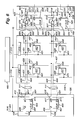
- FIG. 6 shows an embodiment of the invention whereby the FPD configuration is tested at the same time as it is written to.
- Embodiments of the present invention comprise a FPD similar to that described in figure 4, but further is arranged to use the second configuration register latch output 411.
- the elements of figure 6 which are the same as in the preceding figures are referenced by the same reference numbers.
- the second outputs 411 of the configuration registers 403 are output as a second plurality of configuration data lines, running parallel to the first set of configuration data lines and jointly called the configuration data lines 111.
- the switch matrix 115 further comprises a plurality of second configuration data inputs, and switch matrix configuration data lines 503.
- the switch matrix configuration lines 503 are connected on one side of the switch matrix to the second set of configuration lines 111 and on the opposite side are connected to a second set of outputs 505.
- the embodiment of the present invention further comprises an error detection block 543. This may be located in the configuration block or at the end of the processing block.
- the error detection block comprises of a single column of row elements 591, a pull-up device 521, a pull down device 519, and a first output 537.
- Each row element comprises a first test data input 593, a second test data input 595, an Exclusive-NOR (XNOR) gate 597, a transistor switch 513, an error detection latch 525 and a second series of outputs 541.
- XNOR Exclusive-NOR
- the first test data input 593 is connected to a switch matrix output line 439
- the second test data input 595 is connected to a second switch matrix output line 505.
- ach row 591 of the error detection block 543 is arranged whereby both test data input lines are from the same row of switch matrix elements.
- the XNOR gate 597 comprises a first input 507 connected to the first test data input 593, a second input 509 connected to the second test data input 595, and an output 511.
- the error detection latch 525 comprises a first data input connected to the first test data input 593, a second enable input connected to the inverted clock signal as supplied by passing the clock signal 401 through inverter 575, and an output 541.
- the element transistor switch 513 comprises a gate connected to the output of the XNOR gate 597, one of the remaining terminals connected to a common pull-up device 521 and the remaining terminal connected to a common pull-down device 537.
- the test block output 541 is connected to the top of the pull down device.
- the pull-up device 521 and pull-down device is so arranged that the pull-up device is much stronger than the pull-down device, so that if a single transistor conducts the current from the pull up device to the output, the output is pulled up, else the output remains pulled low.
- This circuitry now enables the configuration mode to be incorporated into a comprehensive test scheme.
- This scheme comprises four steps, a scan test, a clock low test, a clock high test and an additional error location test.
- the first step S101 comprises employing a scan of the chip.
- a scan is a method of detecting hardware errors by passing a series of test signals into the input of the circuit and monitoring a series of nodes in the FPD. This is carried out prior to the configuration mode and can be used to test for faults in input circuitry to the configuration data registers, the address registers and any input/output registers.
- the second step s102 is taken during configuration when the clock signal is low.
- the configuration data registers output the value Q onto the configuration data lines 111 and the inverted value /Q onto the second set of configuration data lines 111.
- the value Q is loaded into the selected configuration latches 427, and is also passed as the first input 593 into the error detection block 543.
- the second input 595 into the error detection block is the inverted value /Q. If these two inputs 593,595 are the same an error has occurred.
- the expected inputs 593,595 should be Q and /Q respectively, but in order that the values are the same, in other words either both Q or both /Q, one or other of the values has been corrupted and is wrong.
- This fault can be detected by the XNOR gate 597, which produces a high output when both inputs are the same.
- the switch transistor 513 goes high the switch transistor 513 is closed connecting the pull-up 521 and pull-down 519 devices.
- the error detection block output 537 is brought high, indicating an error. This test is aimed at detecting configuration line 111 or data register output 417 stuck at faults.
- the stuck at fault occurs when a tested node is connected to a voltage level due to some fault in the circuit. It is therefore incapable of changing its voltage level - thus the fault is that the node is stuck at the voltage level independent of the expected voltage.
- the third step S103 occurs when the clock signal is high.
- the configuration register output Q is isolated from the configuration data lines by the configuration register switch 415. Instead the output of the selected configuration latch 427 is output onto the switch matrix configuration data line 425 via the switch matrix switch 435.
- the error detection block first input 593 is the output of the selected configuration latch.
- the error detection block 543 second input 595 is the inverted output of the configuration register latch /Q.
- the XNOR gate activates the transistor switch, which connects the pull-up and pull-down devices, bringing the error detection block output 537 high, indicating an error. This test is aimed at detecting faults within the configuration latch.
- resolution methods may be employed to reject the FPD or to compensate for the fault without rejection of the whole FPD.
- embodiments of the present invention describe a method for testing to be carried out at the same time as configuration.
- Fig 8 shows the enable generation circuitry 419. It comprises a clock input connected to a clock line 401, an enable input connected to the address line 113 connected to the address register 103, a first AND gate 602, a second AND gate 603, a NOT gate 601, a enable input output 421 and an enable output output 423.
- the first AND 602 gate comprises the first input connected to the clock input and a second input connected to the enable input and an output connected to the enable input output.
- the second AND gate 603 comprises the first input connected to an inverted clock input as provided by the output of the NOT gate 601 when the NOT gate input is connected to the clock input, a second input connected to the enable input, and an output connected to the enable output output.
- the enable generation circuit 419 outputs operate only when selected by the address register.
- the two outputs are opposite to each other, with each output value dependent on the value of the clock signal.
- the embodiments of the present invention described above feature the advantages of being able to write configuration data at practically the same time as testing the configuration cycle.
- the embodiments of the present invention also feature the ability to locate and potentially remedy any error in the configuration cycle.
- Embodiments of the present invention may be applied not only to configuration elements in a switch matrix but also to configuration elements in other parts of a FPD which contain configurable elements.
Landscapes
- Physics & Mathematics (AREA)
- Engineering & Computer Science (AREA)
- General Engineering & Computer Science (AREA)
- General Physics & Mathematics (AREA)
- Mathematical Physics (AREA)
- Computer Hardware Design (AREA)
- Computing Systems (AREA)
- Logic Circuits (AREA)
Abstract
Description
Claims (16)
- A field programmable device comprising:a plurality of logic blocks;a plurality of connections connecting said blocks;configuration means for outputting configuration data for programming said device, said configuration means providing at least one pair of outputs; anderror detection means for comparing said outputs to determine if there has been a configuration error.
- A device as claimed in claim 1, wherein said error detecting means comprises means for comparing said outputs.
- A device as claimed in claim 2, wherein said comparing means comprises an XNOR gate.
- A device as claimed in any preceding claim, wherein said error detection means are arranged to determine the presence of an error if a pair of outputs are determined to be the same.
- A device as claimed in any preceding claim, wherein said error detection means comprises at least one transistor arranged to provide a predetermined output when an error is determined.
- A device as claimed in claim 5, wherein said at least one transistor comprises a pull up transistor.
- A device as claimed in any preceding claim, wherein at least one pair of outputs comprise a signal and its inverse.
- A device as claimed in any preceding claim, wherein said error detection means is arranged to determine errors in a first part of said device and then to determine errors on a second part of said device.
- A device as claimed in claim 8, wherein said error detection means is arranged to determine errors in the first part when a clock signal has a first state and to determine errors in the second part when the clock signal has a second state.
- A device as claimed in claim 8 or 9, wherein one of said first and second parts of said device comprises the outputs of said configuration means.
- A device as claimed in any of claims 8 to 10, wherein one of said first and second parts of said device comprises said plurality of connections.
- A device as claimed in any preceding claim, wherein at least one of said logic blocks and said connection means are configurable.
- A device as claimed in any preceding claim, wherein said error detection means is arranged to determine the location of an error.
- A device as claimed in claim 13, wherein said error means comprises means for providing an output for each line of said device.
- A device as claimed in claim 14, wherein said means for providing an output for each line comprise storage means.
- A device as claimed in claim 14 or 15 when appended to claim 2, wherein said means for providing an output for each line comprises said comparing means.
Priority Applications (4)
| Application Number | Priority Date | Filing Date | Title |
|---|---|---|---|
| DE60204539T DE60204539D1 (en) | 2002-04-03 | 2002-04-03 | Field programmable device |
| EP02252426A EP1351065B1 (en) | 2002-04-03 | 2002-04-03 | A field programmable device |
| US10/406,058 US7171599B2 (en) | 2002-04-03 | 2003-04-02 | Field programmable device |
| US12/163,983 USRE42264E1 (en) | 2002-04-03 | 2008-06-27 | Field programmable device |
Applications Claiming Priority (1)
| Application Number | Priority Date | Filing Date | Title |
|---|---|---|---|
| EP02252426A EP1351065B1 (en) | 2002-04-03 | 2002-04-03 | A field programmable device |
Publications (2)
| Publication Number | Publication Date |
|---|---|
| EP1351065A1 true EP1351065A1 (en) | 2003-10-08 |
| EP1351065B1 EP1351065B1 (en) | 2005-06-08 |
Family
ID=27838154
Family Applications (1)
| Application Number | Title | Priority Date | Filing Date |
|---|---|---|---|
| EP02252426A Expired - Lifetime EP1351065B1 (en) | 2002-04-03 | 2002-04-03 | A field programmable device |
Country Status (3)
| Country | Link |
|---|---|
| US (2) | US7171599B2 (en) |
| EP (1) | EP1351065B1 (en) |
| DE (1) | DE60204539D1 (en) |
Cited By (2)
| Publication number | Priority date | Publication date | Assignee | Title |
|---|---|---|---|---|
| CN102508815A (en) * | 2011-10-20 | 2012-06-20 | 大唐移动通信设备有限公司 | Data processing method and system |
| EP2631803A1 (en) * | 2012-02-27 | 2013-08-28 | Altera Corporation | Methods and apparatus for automatic fault detection |
Families Citing this family (6)
| Publication number | Priority date | Publication date | Assignee | Title |
|---|---|---|---|---|
| US7506210B1 (en) | 2003-06-26 | 2009-03-17 | Xilinx, Inc. | Method of debugging PLD configuration using boundary scan |
| US8566616B1 (en) * | 2004-09-10 | 2013-10-22 | Altera Corporation | Method and apparatus for protecting designs in SRAM-based programmable logic devices and the like |
| US8612772B1 (en) | 2004-09-10 | 2013-12-17 | Altera Corporation | Security core using soft key |
| US7480843B1 (en) * | 2004-09-29 | 2009-01-20 | Xilinx, Inc. | Configuration access from a boundary-scannable device |
| US7376872B1 (en) * | 2004-11-01 | 2008-05-20 | Lattice Semiconductor Corporation | Testing embedded memory in integrated circuits such as programmable logic devices |
| US8493089B2 (en) * | 2011-04-06 | 2013-07-23 | International Business Machines Corporation | Programmable logic circuit using three-dimensional stacking techniques |
Citations (4)
| Publication number | Priority date | Publication date | Assignee | Title |
|---|---|---|---|---|
| US5347519A (en) * | 1991-12-03 | 1994-09-13 | Crosspoint Solutions Inc. | Preprogramming testing in a field programmable gate array |
| US5815510A (en) * | 1996-03-28 | 1998-09-29 | Cypress Semiconductor Corp. | Serial programming of instruction codes in different numbers of clock cycles |
| US6300769B1 (en) * | 1999-12-17 | 2001-10-09 | Lsi Logic Corporation | Fast comparator suitable for BIST and BISR applications |
| WO2001086313A1 (en) * | 2000-05-11 | 2001-11-15 | Adaptive Silicon, Inc. | Apparatus and method for self testing programmable logic arrays |
Family Cites Families (14)
| Publication number | Priority date | Publication date | Assignee | Title |
|---|---|---|---|---|
| US5426378A (en) * | 1994-04-20 | 1995-06-20 | Xilinx, Inc. | Programmable logic device which stores more than one configuration and means for switching configurations |
| US6421754B1 (en) * | 1994-12-22 | 2002-07-16 | Texas Instruments Incorporated | System management mode circuits, systems and methods |
| US5640106A (en) * | 1995-05-26 | 1997-06-17 | Xilinx, Inc. | Method and structure for loading data into several IC devices |
| US5768288A (en) * | 1996-03-28 | 1998-06-16 | Cypress Semiconductor Corp. | Method and apparatus for programming a programmable logic device having verify logic for comparing verify data read from a memory location with program data |
| US5789938A (en) * | 1996-09-04 | 1998-08-04 | Xilinx, Inc. | Structure and method for reading blocks of data from selectable points in a memory device |
| US5910732A (en) * | 1997-03-12 | 1999-06-08 | Xilinx, Inc. | Programmable gate array having shared signal lines for interconnect and configuration |
| US6127843A (en) * | 1997-12-22 | 2000-10-03 | Vantis Corporation | Dual port SRAM memory for run time use in FPGA integrated circuits |
| US6237124B1 (en) | 1998-03-16 | 2001-05-22 | Actel Corporation | Methods for errors checking the configuration SRAM and user assignable SRAM data in a field programmable gate array |
| JP2000149564A (en) * | 1998-10-30 | 2000-05-30 | Mitsubishi Electric Corp | Semiconductor storage device |
| US6914449B2 (en) * | 2001-04-02 | 2005-07-05 | Xilinx, Inc. | Structure for reducing leakage current in submicron IC devices |
| EP2051381B1 (en) * | 2002-04-03 | 2011-09-14 | Sicronic Remote KG, LLC | A field programmable device |
| US7007203B2 (en) * | 2002-08-02 | 2006-02-28 | Motorola, Inc. | Error checking in a reconfigurable logic signal processor (RLSP) |
| US7328377B1 (en) * | 2004-01-27 | 2008-02-05 | Altera Corporation | Error correction for programmable logic integrated circuits |
| US7263631B2 (en) * | 2004-08-13 | 2007-08-28 | Seakr Engineering, Incorporated | Soft error detection and recovery |
-
2002
- 2002-04-03 EP EP02252426A patent/EP1351065B1/en not_active Expired - Lifetime
- 2002-04-03 DE DE60204539T patent/DE60204539D1/en not_active Expired - Lifetime
-
2003
- 2003-04-02 US US10/406,058 patent/US7171599B2/en not_active Expired - Lifetime
-
2008
- 2008-06-27 US US12/163,983 patent/USRE42264E1/en not_active Expired - Fee Related
Patent Citations (4)
| Publication number | Priority date | Publication date | Assignee | Title |
|---|---|---|---|---|
| US5347519A (en) * | 1991-12-03 | 1994-09-13 | Crosspoint Solutions Inc. | Preprogramming testing in a field programmable gate array |
| US5815510A (en) * | 1996-03-28 | 1998-09-29 | Cypress Semiconductor Corp. | Serial programming of instruction codes in different numbers of clock cycles |
| US6300769B1 (en) * | 1999-12-17 | 2001-10-09 | Lsi Logic Corporation | Fast comparator suitable for BIST and BISR applications |
| WO2001086313A1 (en) * | 2000-05-11 | 2001-11-15 | Adaptive Silicon, Inc. | Apparatus and method for self testing programmable logic arrays |
Cited By (6)
| Publication number | Priority date | Publication date | Assignee | Title |
|---|---|---|---|---|
| CN102508815A (en) * | 2011-10-20 | 2012-06-20 | 大唐移动通信设备有限公司 | Data processing method and system |
| CN102508815B (en) * | 2011-10-20 | 2014-10-08 | 大唐移动通信设备有限公司 | Data processing method and system |
| EP2631803A1 (en) * | 2012-02-27 | 2013-08-28 | Altera Corporation | Methods and apparatus for automatic fault detection |
| CN103294048A (en) * | 2012-02-27 | 2013-09-11 | 阿尔特拉公司 | Methods and apparatuses for automatic fault detection |
| US9235460B2 (en) | 2012-02-27 | 2016-01-12 | Altera Corporation | Methods and apparatus for automatic fault detection |
| US9360522B2 (en) | 2012-02-27 | 2016-06-07 | Altera Corporation | Methods and apparatus for automatic fault detection |
Also Published As
| Publication number | Publication date |
|---|---|
| USRE42264E1 (en) | 2011-03-29 |
| US20030221151A1 (en) | 2003-11-27 |
| EP1351065B1 (en) | 2005-06-08 |
| DE60204539D1 (en) | 2005-07-14 |
| US7171599B2 (en) | 2007-01-30 |
Similar Documents
| Publication | Publication Date | Title |
|---|---|---|
| US6201404B1 (en) | Programmable logic device with redundant circuitry | |
| US7216277B1 (en) | Self-repairing redundancy for memory blocks in programmable logic devices | |
| US5083083A (en) | Testability architecture and techniques for programmable interconnect architecture | |
| USRE42264E1 (en) | Field programmable device | |
| US5365165A (en) | Testability architecture and techniques for programmable interconnect architecture | |
| US7212448B1 (en) | Method and apparatus for multiple context and high reliability operation of programmable logic devices | |
| US5223792A (en) | Testability architecture and techniques for programmable interconnect architecture | |
| US4293919A (en) | Level sensitive scan design (LSSD) system | |
| US5208530A (en) | Testability architecture and techniques for programmable interconnect architecture | |
| US5309091A (en) | Testability architecture and techniques for programmable interconnect architecture | |
| US8065574B1 (en) | Soft error detection logic testing systems and methods | |
| US5341092A (en) | Testability architecture and techniques for programmable interconnect architecture | |
| US7167404B2 (en) | Method and device for testing configuration memory cells in programmable logic devices (PLDS) | |
| US20050039098A1 (en) | Apparatus and method for self testing programmable logic arrays | |
| US7786749B1 (en) | Programmable integrated circuit having built in test circuit | |
| US6968478B1 (en) | Method and apparatus for data transfer validation | |
| US20180301201A1 (en) | Methods and apparatus for detecting defects in memory circuitry | |
| US7301836B1 (en) | Feature control circuitry for testing integrated circuits | |
| US7225373B1 (en) | Data transfer validation system | |
| US7266020B1 (en) | Method and apparatus for address and data line usage in a multiple context programmable logic device | |
| US7250786B1 (en) | Method and apparatus for modular redundancy with alternative mode of operation | |
| US8091001B2 (en) | FPGA programming structure for ATPG test coverage | |
| US12217811B2 (en) | Programmable logic device with design for test functionality | |
| US4682331A (en) | Logic circuit with self-test | |
| EP2051381B1 (en) | A field programmable device |
Legal Events
| Date | Code | Title | Description |
|---|---|---|---|
| PUAI | Public reference made under article 153(3) epc to a published international application that has entered the european phase |
Free format text: ORIGINAL CODE: 0009012 |
|
| AK | Designated contracting states |
Kind code of ref document: A1 Designated state(s): AT BE CH CY DE DK ES FI FR GB GR IE IT LI LU MC NL PT SE TR |
|
| AX | Request for extension of the european patent |
Extension state: AL LT LV MK RO SI |
|
| 17P | Request for examination filed |
Effective date: 20040405 |
|
| 17Q | First examination report despatched |
Effective date: 20040429 |
|
| AKX | Designation fees paid |
Designated state(s): DE FR GB IT |
|
| GRAP | Despatch of communication of intention to grant a patent |
Free format text: ORIGINAL CODE: EPIDOSNIGR1 |
|
| GRAS | Grant fee paid |
Free format text: ORIGINAL CODE: EPIDOSNIGR3 |
|
| GRAA | (expected) grant |
Free format text: ORIGINAL CODE: 0009210 |
|
| AK | Designated contracting states |
Kind code of ref document: B1 Designated state(s): DE FR GB IT |
|
| PG25 | Lapsed in a contracting state [announced via postgrant information from national office to epo] |
Ref country code: IT Free format text: LAPSE BECAUSE OF FAILURE TO SUBMIT A TRANSLATION OF THE DESCRIPTION OR TO PAY THE FEE WITHIN THE PRESCRIBED TIME-LIMIT;WARNING: LAPSES OF ITALIAN PATENTS WITH EFFECTIVE DATE BEFORE 2007 MAY HAVE OCCURRED AT ANY TIME BEFORE 2007. THE CORRECT EFFECTIVE DATE MAY BE DIFFERENT FROM THE ONE RECORDED. Effective date: 20050608 |
|
| REG | Reference to a national code |
Ref country code: GB Ref legal event code: FG4D |
|
| REF | Corresponds to: |
Ref document number: 60204539 Country of ref document: DE Date of ref document: 20050714 Kind code of ref document: P |
|
| PG25 | Lapsed in a contracting state [announced via postgrant information from national office to epo] |
Ref country code: DE Free format text: LAPSE BECAUSE OF FAILURE TO SUBMIT A TRANSLATION OF THE DESCRIPTION OR TO PAY THE FEE WITHIN THE PRESCRIBED TIME-LIMIT Effective date: 20050909 |
|
| ET | Fr: translation filed | ||
| PLBE | No opposition filed within time limit |
Free format text: ORIGINAL CODE: 0009261 |
|
| STAA | Information on the status of an ep patent application or granted ep patent |
Free format text: STATUS: NO OPPOSITION FILED WITHIN TIME LIMIT |
|
| 26N | No opposition filed |
Effective date: 20060309 |
|
| REG | Reference to a national code |
Ref country code: GB Ref legal event code: 732E |
|
| REG | Reference to a national code |
Ref country code: FR Ref legal event code: TP Ref country code: FR Ref legal event code: CJ |
|
| PGFP | Annual fee paid to national office [announced via postgrant information from national office to epo] |
Ref country code: GB Payment date: 20120327 Year of fee payment: 11 |
|
| PGFP | Annual fee paid to national office [announced via postgrant information from national office to epo] |
Ref country code: FR Payment date: 20120503 Year of fee payment: 11 |
|
| GBPC | Gb: european patent ceased through non-payment of renewal fee |
Effective date: 20130403 |
|
| PG25 | Lapsed in a contracting state [announced via postgrant information from national office to epo] |
Ref country code: GB Free format text: LAPSE BECAUSE OF NON-PAYMENT OF DUE FEES Effective date: 20130403 |
|
| REG | Reference to a national code |
Ref country code: FR Ref legal event code: ST Effective date: 20131231 |
|
| PG25 | Lapsed in a contracting state [announced via postgrant information from national office to epo] |
Ref country code: FR Free format text: LAPSE BECAUSE OF NON-PAYMENT OF DUE FEES Effective date: 20130430 |