EP1347706B1 - Electrical impedance tomography - Google Patents
Electrical impedance tomography Download PDFInfo
- Publication number
- EP1347706B1 EP1347706B1 EP01272705A EP01272705A EP1347706B1 EP 1347706 B1 EP1347706 B1 EP 1347706B1 EP 01272705 A EP01272705 A EP 01272705A EP 01272705 A EP01272705 A EP 01272705A EP 1347706 B1 EP1347706 B1 EP 1347706B1
- Authority
- EP
- European Patent Office
- Prior art keywords
- contacts
- ring
- electrode
- distribution
- electrical
- Prior art date
- Legal status (The legal status is an assumption and is not a legal conclusion. Google has not performed a legal analysis and makes no representation as to the accuracy of the status listed.)
- Expired - Lifetime
Links
- 238000002593 electrical impedance tomography Methods 0.000 title description 10
- 238000000034 method Methods 0.000 claims abstract description 66
- 238000009826 distribution Methods 0.000 claims abstract description 53
- 239000007787 solid Substances 0.000 claims abstract description 6
- 238000012545 processing Methods 0.000 claims abstract description 3
- 238000005259 measurement Methods 0.000 claims description 43
- 239000012530 fluid Substances 0.000 claims description 15
- 230000008569 process Effects 0.000 claims description 14
- 239000002184 metal Substances 0.000 claims description 4
- 229910052751 metal Inorganic materials 0.000 claims description 4
- 239000000126 substance Substances 0.000 claims description 4
- XUIMIQQOPSSXEZ-UHFFFAOYSA-N Silicon Chemical compound [Si] XUIMIQQOPSSXEZ-UHFFFAOYSA-N 0.000 claims description 2
- 239000000919 ceramic Substances 0.000 claims description 2
- 230000007274 generation of a signal involved in cell-cell signaling Effects 0.000 claims 2
- 230000035945 sensitivity Effects 0.000 abstract description 60
- 238000003384 imaging method Methods 0.000 abstract description 16
- 230000005684 electric field Effects 0.000 abstract description 10
- 239000000463 material Substances 0.000 abstract description 8
- 239000011159 matrix material Substances 0.000 description 35
- 239000000243 solution Substances 0.000 description 33
- 239000013598 vector Substances 0.000 description 21
- 239000012071 phase Substances 0.000 description 17
- 230000008859 change Effects 0.000 description 16
- 238000004422 calculation algorithm Methods 0.000 description 14
- 238000010276 construction Methods 0.000 description 11
- 230000005284 excitation Effects 0.000 description 11
- XLYOFNOQVPJJNP-UHFFFAOYSA-N water Substances O XLYOFNOQVPJJNP-UHFFFAOYSA-N 0.000 description 8
- 238000004088 simulation Methods 0.000 description 7
- 230000015572 biosynthetic process Effects 0.000 description 6
- 239000003792 electrolyte Substances 0.000 description 5
- 238000002474 experimental method Methods 0.000 description 4
- 239000006260 foam Substances 0.000 description 4
- 238000004519 manufacturing process Methods 0.000 description 4
- 238000003325 tomography Methods 0.000 description 4
- 238000013459 approach Methods 0.000 description 3
- 230000005587 bubbling Effects 0.000 description 3
- 230000000694 effects Effects 0.000 description 3
- 238000004070 electrodeposition Methods 0.000 description 3
- 239000007788 liquid Substances 0.000 description 3
- 238000012360 testing method Methods 0.000 description 3
- 230000008901 benefit Effects 0.000 description 2
- 239000012267 brine Substances 0.000 description 2
- 230000008878 coupling Effects 0.000 description 2
- 238000010168 coupling process Methods 0.000 description 2
- 238000005859 coupling reaction Methods 0.000 description 2
- 238000005520 cutting process Methods 0.000 description 2
- 238000005516 engineering process Methods 0.000 description 2
- 238000009434 installation Methods 0.000 description 2
- 238000002156 mixing Methods 0.000 description 2
- 238000010606 normalization Methods 0.000 description 2
- 239000003921 oil Substances 0.000 description 2
- 230000035479 physiological effects, processes and functions Effects 0.000 description 2
- 230000004044 response Effects 0.000 description 2
- 238000000926 separation method Methods 0.000 description 2
- HPALAKNZSZLMCH-UHFFFAOYSA-M sodium;chloride;hydrate Chemical compound O.[Na+].[Cl-] HPALAKNZSZLMCH-UHFFFAOYSA-M 0.000 description 2
- 230000005514 two-phase flow Effects 0.000 description 2
- YTBRNEUEFCNVHC-UHFFFAOYSA-N 4,4'-dichlorobiphenyl Chemical compound C1=CC(Cl)=CC=C1C1=CC=C(Cl)C=C1 YTBRNEUEFCNVHC-UHFFFAOYSA-N 0.000 description 1
- 238000002940 Newton-Raphson method Methods 0.000 description 1
- NIXOWILDQLNWCW-UHFFFAOYSA-N acrylic acid group Chemical group C(C=C)(=O)O NIXOWILDQLNWCW-UHFFFAOYSA-N 0.000 description 1
- 230000002238 attenuated effect Effects 0.000 description 1
- 238000004364 calculation method Methods 0.000 description 1
- 239000011248 coating agent Substances 0.000 description 1
- 238000000576 coating method Methods 0.000 description 1
- 238000004590 computer program Methods 0.000 description 1
- 230000003750 conditioning effect Effects 0.000 description 1
- 239000004020 conductor Substances 0.000 description 1
- 238000002939 conjugate gradient method Methods 0.000 description 1
- 230000007423 decrease Effects 0.000 description 1
- 230000003247 decreasing effect Effects 0.000 description 1
- 238000009795 derivation Methods 0.000 description 1
- 238000013461 design Methods 0.000 description 1
- 238000010586 diagram Methods 0.000 description 1
- 238000009543 diffuse optical tomography Methods 0.000 description 1
- 238000010292 electrical insulation Methods 0.000 description 1
- 238000002347 injection Methods 0.000 description 1
- 239000007924 injection Substances 0.000 description 1
- 238000007689 inspection Methods 0.000 description 1
- 239000007791 liquid phase Substances 0.000 description 1
- 238000013507 mapping Methods 0.000 description 1
- 230000007246 mechanism Effects 0.000 description 1
- 239000007769 metal material Substances 0.000 description 1
- 150000002739 metals Chemical class 0.000 description 1
- 239000012811 non-conductive material Substances 0.000 description 1
- 238000009828 non-uniform distribution Methods 0.000 description 1
- 238000005192 partition Methods 0.000 description 1
- 239000004033 plastic Substances 0.000 description 1
- 239000000843 powder Substances 0.000 description 1
- 238000003672 processing method Methods 0.000 description 1
- 229910052710 silicon Inorganic materials 0.000 description 1
- 239000010703 silicon Substances 0.000 description 1
- 239000008399 tap water Substances 0.000 description 1
- 235000020679 tap water Nutrition 0.000 description 1
- 230000000007 visual effect Effects 0.000 description 1
- 238000012800 visualization Methods 0.000 description 1
Images


Classifications
-
- G—PHYSICS
- G01—MEASURING; TESTING
- G01N—INVESTIGATING OR ANALYSING MATERIALS BY DETERMINING THEIR CHEMICAL OR PHYSICAL PROPERTIES
- G01N27/00—Investigating or analysing materials by the use of electric, electrochemical, or magnetic means
- G01N27/02—Investigating or analysing materials by the use of electric, electrochemical, or magnetic means by investigating impedance
- G01N27/22—Investigating or analysing materials by the use of electric, electrochemical, or magnetic means by investigating impedance by investigating capacitance
- G01N27/24—Investigating the presence of flaws
-
- G—PHYSICS
- G01—MEASURING; TESTING
- G01N—INVESTIGATING OR ANALYSING MATERIALS BY DETERMINING THEIR CHEMICAL OR PHYSICAL PROPERTIES
- G01N27/00—Investigating or analysing materials by the use of electric, electrochemical, or magnetic means
- G01N27/02—Investigating or analysing materials by the use of electric, electrochemical, or magnetic means by investigating impedance
- G01N27/04—Investigating or analysing materials by the use of electric, electrochemical, or magnetic means by investigating impedance by investigating resistance
- G01N27/20—Investigating the presence of flaws
-
- A—HUMAN NECESSITIES
- A61—MEDICAL OR VETERINARY SCIENCE; HYGIENE
- A61B—DIAGNOSIS; SURGERY; IDENTIFICATION
- A61B5/00—Measuring for diagnostic purposes; Identification of persons
- A61B5/05—Detecting, measuring or recording for diagnosis by means of electric currents or magnetic fields; Measuring using microwaves or radio waves
- A61B5/053—Measuring electrical impedance or conductance of a portion of the body
- A61B5/0536—Impedance imaging, e.g. by tomography
Definitions
- This invention relates to a method of measuring the distribution of electrical impedance of a multi-phase flow using an electrically conductive ring electrode, and to a method of determining the internal of a body which utilises such a method.
- the invention further relates to an apparatus adapted to measure the distribution of electrical impedance of a multi-phase flow using an electrically conductive ring electrode.
- This invention relates in general to electrical impedance tomography (EIT), and in particular to a new sensor construction and apparatus, a sensing strategy and an algorithm for measuring flow with electrically continuous and discontinuous conductivity phase, such as the oil/gas/water multiphase flow and the bubbling formation or foam construction.
- EIT electrical impedance tomography
- a number of sensor construction methods for EIT were proposed in previous patents, which comprised placing an array of spaced electrodes in direct contact with the human body or process fluid [ GB2119520 , GB2160323 , US4617939 ], or in indirect contact with the human body coupled with electrolyte [ GB2019579 ], a sponger [ WO98/23204 ] or any other suitable liquid medium [ US4486835 ] with conductivity matched to the typical expected conductivity of the object being measured.
- a correct measurement cannot be provided from a fluid with a discontinuous phase of electrical conductivity, since some of these electrodes have lost their electrical contact with the conductive phase of the fluid, e.g. a half filled horizontal stratified flow or a foam construction with a large bubbling formation [ M. Wang and C. J. Young, Chem. Eng. Science, 54(5), 1999 ].
- the discrete electrode structure generates a very non-uniform distribution of the imaging sensitivity because high dense currents are always present at the domains near to the current injecting and sinking electrodes.
- the limited contact area of the electrodes also produces a large common voltage, which greatly reduces the signal-to-noise ratio for the differential measurement adopted in most cases.
- the major features of this invention are to employ an electrically conductive ring with a conductivity value higher than that of the principle flow [ Figure 1 ] as a tomographic sensor to supply a continuously electric current flow to the sensing domain, generate a more homogeneous imaging sensitivity distribution over the sensing domain and provide a smooth sensing surface without the obstruction effects to the flow.
- a ⁇ /2 sensing strategy further improves the imaging sensitivity distribution and an image reconstruction algorithm provides a practical solution for eliminating hardware noise in EIT applications.
- the object of the invention is to provide a sensing method and apparatus with an improved imaging sensitivity distribution for measuring the electrical impedance distribution in a principle flow with an electrically continuous or discontinuous phase and a practically applicable accurate reconstruction algorithm for flow measurement.
- the ring electrode may have a much higher conductivity compared to the principle flow or materials to be measured and it is employed as said a ring electrode of a part of the sensor body. A more homogeneous electric field distribution can be produced if the conductivity of the electrical conductive ring is much higher than that of the target content.
- the electrically conductive ring may be made of solid substances such as a kind of metal, conductive rubber or ceramics.
- a number of electrical contacts may be penetrated through the wall of the ring electrode in good electrical contact with the wall of the ring.
- the size of the contacts can be very small and the amount of the contacts can be installed to be much more than those in previous sensors.
- the sensitivity distribution is relatively intensified at a particular area of interest within the whole sensing domain, based on a specific sensing strategy or a combination of a basic set of independent measurements.
- the sensor geometry and its conductivity can be optimized for the objective that the condition number of the sensitivity matrix becomes less and the sensitivity field becomes more homogenous.
- the method of the invention may be especially useful in determining the structure of, for example, process materials, such as a process fluid or a part of a human body, with electrically continuous phase such as that a miscible liquid or discontinuous phase such as that in a foam formation or a half filled horizontal oil/water/gas stratified flow.
- process materials such as a process fluid or a part of a human body
- electrically continuous phase such as that a miscible liquid or discontinuous phase such as that in a foam formation or a half filled horizontal oil/water/gas stratified flow.
- the method may be extended to a sensor with discrete electrode structure using an external resistor network connecting all electrodes. Furthermore a multi-step image reconstruction algorithm using an error processing method is employed to reconstruct the conductivity distribution.
- s j,k denotes the sensitivity coefficient at pixel k under the measurement-projection j
- P denotes the maximum number of measurements
- w denotes the maximum number of pixels
- ⁇ k and ⁇ k are the conductivity and conductivity change at pixel k , respectively
- V j and ⁇ V j are in respect to the reference voltage and the voltage change at measurement-projection j .
- An apparatus adapted to measure the distribution of electrical impedance of a multi-phase flow is defined in claim 8.
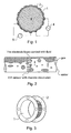
- the electrically conductive ring sensor basically consists of an electrically conductive ring 1, a number of electrical contacts 2, a target content 3, a number of electrical excitation sources 4 and a number of voltage measurement devices 5 [ Figure 1 ].
- the electrically conductive ring 1 is made of solid substances such as a kind of metals or alternatively, other electrically conductive materials such as conductive rubber or ceramic-metal with a conductivity value much higher than that of the content 3 to be measured.
- the electrically conductive ring acts as an 'continuous electrode' to distribute the electrical current flow and generate an electric field for mapping the impedance distribution of the content 3 due to applying currents from the metallic contacts 2.
- the metallic contacts 2 are embedded into the electrically conductive ring in good electrical contact with the outside wall of the electrically conductive ring.
- the size of these contacts 2 may be very small since a low common voltage on the contacts is produced from the high conductive ring 1 and there are no effects of electrode-electrolyte interface between these contacts 2 and the electrically conductive ring 1 if the ring is made of solid substance. Therefore, the number of the contacts to be installed could be much more than the number of discrete electrodes in the conventional sensors.
- a number of electrical excitation sources such as the currents or voltages 4 are applied to one or more electrical contacts 2. Boundary voltages or currents are also measured from the electrical contacts 2.
- a continuous electric field distribution presents along the inner surface of the electrically conductive ring that is in electrical contact with the target content 3.
- the target content 3 may be a process fluid with electrically continuous phase, such as that in a miscible liquid mixing, or with electrically discontinuous phases, such as those in oil-water-gas flow or froth formation [ figure 2 ]. Since no discrete electrode directly contacts the target content 3, the excitation and measurement will not get into saturation under a certain current value when a part of the inner sensing surface loses an electrical contact to the principle flow.
- Figure 3 illustrates its flange configuration.
- a more homogeneous electric field distribution can be produced if the conductivity of the electrically conductive ring 1 is higher than that of the target content 3.
- Comparisons of the potential distributions generated from a sensor with discrete electrodes ( Figure 4a and 4b ) and the electrically conductive ring sensor ( Figure 5a and 5b ) are given, which were simulated using Ansoft Maxwell 2D simulator [Version 1-7-66, 1996, Ansoft Corporation]. In the simulation, the conductivity of the electrically conductive ring was ten times as that of the target content.
- the potential distributions in Figure 4a and 5a were generated from a current excitation between an adjacent electrode/contact pair.
- Figure 4b and 5b are potential distributions relating to an opposite electrode/contact pair excitation position.
- the resistor network 9 plays a similar role as the electrically conductive ring 1, which bypasses and re-distributes currents in case of the current excitation electrodes blocked by a discontinuous fluid or bubbles, and produces a more homogeneous electric field than that produced from a conventional discrete electrode sensor.
- Figure 6 shows the extension for the sensor with discrete electrodes.
- the measurement relationship between one and other sensing strategies for a 4-electrode measurement protocol can be derived as Equation 1 & 2 based on the reciprocity theorem [Geselowitz, IEEE Trans. Biomed. Eng. BME-18], which may be summarised as 'with a 4-electrode measurement protocol, the boundary measurements and the sensitivity matrix for an alternative sensing strategy can be derived from the complete set of independent measurements and the sensitivity matrix obtained from a known sensing strategy'.
- the measurements based on the alternative sensing strategy can not generate any more new information than that given from the complete set of independent measurements, but could produce a different signal-to-noise ratio and a different sensitivity distribution over the imaging domain.
- Equation 1 A general form of the boundary voltage relationship between an alternative 4-electrode sensing strategy and adjacent sensing strategy can be expressed as Equation 1, which derives mutual impedance or boundary voltages for an alternative 4-electrode sensing strategy from those for adjacent electrode pair strategy.
- Z I,J ( I M,N ) represents the mutual impedance obtained from voltage measured between electrodes I and J when current presents between electrodes M and N .
- the sensitivity matrix of an alternative sensing strategy can also be derived from algebraic combination of the sensitivity matrix obtained from a complete set of independent measurements because a linear approximation is adopted in the calculation of the sensitivity matrix, and the linear relationship between the two sets of boundary voltages exist (Equation 1). Derivation to a new sensitivity matrix for an alternative strategy from the sensitivity matrix of adjacent electrode pair strategy is given in Equation 2.
- S I,J ( I M,N ) represents the sensitivity coefficient at pixel, k , obtained from the measurement and excitation position where the voltage is measured between electrodes I and J when current presents between electrodes M and N .
- Figure 8 gives a more homogenous sensitivity band across the central area, compared to Figure 10 .
- the overall sensitivity distribution in Figure 9 is more homogenous as well, compared to that given in Figure 11 , which demonstrates that a much improved total-sensitivity distribution over the sensing area has been produced.
- the results of the alternative sensing strategy imply that the imaging sensitivity can be relatively intensified or attenuated at a particulate interested area in the whole imaging domain.
- the sensitivity matrix for such specific distribution can be derived from either the alternative sensing strategy or the particulate combination of the sensitivity matrix derived from a known basic set of independent measurements (e.g. adjacent electrode pair sensing strategy).
- the sensor geometry and its conductivity value can be further optimised. It is found that the ill conditioning of the sensitivity matrix (essentially Jacobean matrix) is related to the non-homogeneity of the sensitivity field. The bigger the condition number of the sensitivity matrix is, the more non-homogeneous the sensitivity field is. The smallest sensitivity is related to the central elements with largest related to periphery elements [ Yorkey, et al, IEEE Trans. Biomed. Eng., BME 34(11), 1987 ]. Taking the condition number as the optimum objective, we can optimize the conductive ring sensor against different thickness and conductivity of the conductive ring sensor.
- Figure 12 shows the sensor geometry used during the optimum design.
- sixteen electrical contacts are distributed around the conductive ring, possessing half of the circumference of the external side of the ring.
- the ring itself has an internal diameter of 5cm.
- the conductive ring thickness, t was varied during the simulations.
- the value of t was assumed to be 0.2cm, 0.6cm, 0.8cm, and 1.0cm.
- the conductivity of the ring is also a variable ranging from 0.11ms/cm to 0.66ms/cm.
- the sensor was assumed filled with water with a conductivity of 0, 11ms/cm.
- FIG. 13 A comparison of sensitivity distribution across the diameter is shown in figure 13 , where the current is injected from electrode 1, and 2 with measurements taken from electrodes 9 and 10.
- the distribution in the conductive ring sensor is more homogenous than that in traditional sensors.
- the important parameters are the ratio of the conductivity and thickness of the ring to those of the material filling the sensor, rather than their absolute values.
- the numerical results for one case could be obtained from another case by appropriate scaling if the same conductivity and thickness ratio were used in simulations.
- a sensitivity matrix for a commonly used adjacent sensing protocol [ Brown et al, Proc. IEE Int. Conf. on Electric and Magnetic field in Med. and Bio, 1985 ] is computed and condition number calculated for each conductivity and thickness value.
- Figure 14 shows the distribution of the condition number of the sensitivity matrix when the thickness and conductivity of the conductive ring sensor varies.
- the illness measure is not a monotonously decreasing function of the thickness and conductivity of the conductive ring sensor.
- the condition number curve is shown in Figure 15 . It is found that the illness measure reaches its minimum at the conductivity of 0.66ms/cm.
- the optimal parameters of the conductive ring should be 0.55ms/cm and 4mm for the conductivity and the thickness respectively.
- the senor can also be constructed from a conductive disk 11. A hole is drilled in the center of the disk and a layer of metallic coating serving as electrode contacts 2 is made around the ring. [ Figure 16a ].
- the disk shape sensor can also be configured into a flange or a washer from 18 [ Figure 16c ].
- PCB 15 can be made to integrate the electrical contacts 2, wiring 13 and connector 12 [ Figure 16b ]. Another advantage of this configuration is its flexibility for replacing the conductive ring once it is contaminated such as in food or pharmaceutical applications.
- the conductive sensor can be made in a micro- or nanoscale using micro-machine technology or integrated circuit fabrication technologies.
- the sensor can also be fabricated integrated with its processing circuits on a single silicon chip.
- Equation 3 Murai, et al, IEEE Trans. BME-32, 1985
- Equation 4 Wang, et al, Chem. Eng. Comm. V 175, 1999 ], assuming the conductivity change is much smaller than the original value ( ⁇ k ⁇ ⁇ k ) and neglecting the high order terms and supposing that the conductivity distribution is composed from w small uniform 'patches' or pixels.
- Equation 5 Murai, et al, IEEE Trans. BME-32, 1985 ], where ⁇ k is a discrete area at k .
- ⁇ AB , ⁇ CD are potentials measured from ports A-B and C-D in response to the present of currents I ⁇ and I ⁇ ⁇ , respectively.
- s j,k denotes the sensitivity coefficient at pixel k under the measurement-projection j
- P denotes the maximum number of measurements
- w denotes the maximum number of pixels
- ⁇ k and ⁇ k are the conductivity and conductivity change at pixel k , respectively
- V j and ⁇ V j are in respect to the reference voltage and the voltage change at measurement-projection j .
- Forward solution in the multi-step inverse solution is used for producing an error vector for each step inversion. It also updates the sensitivity matrix for next step inverse solution.
- Sensitivity matrix can be derived directly from the nodal voltages obtained from the forward solution [ Yorkey, et al, IEEE Trans, BME-34, 1987 , Murai, et al, IEEE Trans. BME-32, 1985 ].
- the actual current value used in the solution is not significant as long as the value does not vary over the whole process since only relative changes of the boundary voltage measurements are employed in following inverse solution.
- Equation 7 The solution of a FEM model presenting a 2D cross-section of a process vessel with Neumann boundary conditions in addition to a single Dirichlet condition to avoid singularity can be solved by Equation 7 utilising a linear approximation given by Yorkey et al and Murai et al.[ Yorkey, et al, IEEE Trans. BME-34,1987 , Murai, et al, . IEEE Trans. BME-32, 1985 ].
- Yv c where Y, v, c denotes the global conductance matrix, the nodal voltage vector, and the nodal current vector respectively.
- the conductivity updating also can be based on an approximation of the inverse relation (Eq.13 based on 1+x ⁇ 1 / (1-x) at x ⁇ 1), which can improve the convergence speed for both positive and negative changes in conductivity.
- the decomposed boundary relative change or error vector in Eq.14 will be minimised. It is thought the non-linear inverse solution has been reached when the norm of the error vector is sufficiently small.
- the sensitivity coefficient back-projection approximation method utilising a normalised transpose matrix of the sensitivity matrix obtained from Eq.5 as a weighting matrix, was first refined for ERT by Kotre [ Kotre, Physiology Measurements, 15, Supp. 2A 1992 ].
- the approximation has been successfully applied to many industrial applications [ Williams et al, Process tomography-principles, techniques and applications, Butterworth-Heinemann Ltd., 1995 ] due to its good anti-noise capability and fast solution speed.
- the physical definition may follow the basic principle of linear back projection: the relative change of the boundary voltage measurements is linearly back-projected to each pixel between two equipotential lines in the case of the equipotential back projection [ Baber et al, Applied potential tomography', J. Phys. E: Sci. Instrum., 17,1984 ], or over whole domain in the case of the SBP [ Kotre, Physiology Measurements, 15, Suppl. 2A 1992 ].
- the sum of the products of the relative change and the weight factor/sensitivity coefficient at each pixel normalised by the sum of their weight factors/sensitivity coefficients that are derived from all possible boundary measurements, approximately presents the relative change of the conductivity at this pixel.
- FIG.18a A set-up with a complex conductivity distribution, as shown in Fig.18a , is reconstructed as Figs. 18b and 18c from the SBP and EIDORS algorithms respectively. It is obvious that the SBP algorithm could not deliver an accurate image for this set-up ( Fig. 18b ). Both the EIDORS ( Fig.18c ) and SCG ( Fig.18d & f ) can reconstruct the complexity of the set-up. The image obtained from five steps of the SCG solution ( Fig.18c ) provides a conductivity error of 3.32% and a boundary voltage error of 0.055%. The discretisation error caused by applying different mesh is reflected in Fig.3f .
- Fig.19 Imaging distinguishability of these algorithms was investigated and the results are given in Fig.19 .
- Two 'objects' were located along a radius of a mesh ( Fig.19a ).
- SBP can image the presence of the two objects but could not distinguish them ( Fig.19b ).
- the edge of the objects' image is also merged with the boundary.
- the image obtained from EIDORS ( Fig. 19c ) gives a better presentation about the object location with a clear separation from the boundary but is incapable of distinguishing between the two objects.
- SCG can clearly distinguish between the two objects although a certain artificial background noise presents ( Fig.19d & f ).
- the single step method solution is be further simplified by obtaining an approximation of the inverse of s ( s is the normalised sensitivity matrix) and therefore the whole computation for reconstructing a single image only involves a multiplication of a matrix and a vector.
- s is the normalised sensitivity matrix
- equation (16) cannot be solved using direct inverse method aiming to an accurate solution.
- An iterative method with finite steps gives equation (16) an approximation solution, which serves as a kind of regularization.
- iterative methods involves much larger computation load than direct inverse methods by which an inverse matrix for s T s can be obtained, and the solution to equation (16) only involves a multiplication of a matrix ( s T s ) -1 ⁇ s T with an vector e.
- a * x ⁇ 1 1 0 . . . 0
- a * x ⁇ 2 0 1 . . . 0
- a * x ⁇ 3 0 0 1 . . 0 , ... ... ... ...
- a * xn 0 0 . . . 1
- Multiphase flow exists in many industrial processes.
- the phase distribution and interfaces in a multiphase flow carries significant information about the processes [ Chhabra et al, Non-newtonian flow in the process industries - fundamentals and engineering applications, Butterworth-Heinemann, Oxford, 1999 ].
- its behaviour is extremely complex, which presents a great challenge to the study of the flow mechanisms and the measurement of multiphase flow.
- Both single modality and multi-modality imaging have been reported [ Dyakowski et al, Powder Technol. 104, 1999 ; Hoyle et al, Proc. 1st World Congress on Industrial Process Tomography, Buxton, UK, 1999 ] as a means to identify flow regimes in two-phase flow.
- A.20 m flow loop (inner diameter, 50mm) fitted with ERT sensors was employed for the experiments.
- a schematic diagram and overview of the flow loop are given in Figure 20 .
- Mains tap-water (conductivity 0.304mS/cm) was used as the liquid phase and air, were introduced into the flow loop from a mixing jet-pump. Measurements were performed at ambient temperature. By controlling the air flowrate at the air inlet of the jet-pump, different flow regimes were generated in the low part of the flow loop.
- the experiments were performed under different air flow-rates of 0.5m 3 /h, 1.5m 3 /h, 2.5m 3 /h, 3.5m 3 /h and the one less than 0.5m 3 /h in regard to the productions of slug flow, slug-churn flow, churn flow and bubbly flow regimes.
- the water flows were scaled with an accumulating tank during the experiments to get water flow rate and mean velocity. At the mean time, a number of photographs were recorded as visual presentations of these different flow regimes.
- Two-dimensional (2D) slice images were sequentially reconstructed. Some reconstructed images in respect to typical air cavities in the flow loop are shown in Figure 21 , where the blue areas represent the air cavities or low conductivity regions and the red areas represent the water or high conductivity regions.
Landscapes
- Chemical & Material Sciences (AREA)
- General Health & Medical Sciences (AREA)
- Immunology (AREA)
- Physics & Mathematics (AREA)
- Health & Medical Sciences (AREA)
- Life Sciences & Earth Sciences (AREA)
- Analytical Chemistry (AREA)
- Biochemistry (AREA)
- Chemical Kinetics & Catalysis (AREA)
- Electrochemistry (AREA)
- Pathology (AREA)
- General Physics & Mathematics (AREA)
- Investigating Or Analyzing Materials By The Use Of Electric Means (AREA)
- Medicines Containing Antibodies Or Antigens For Use As Internal Diagnostic Agents (AREA)
- Ultra Sonic Daignosis Equipment (AREA)
- Materials For Medical Uses (AREA)
- Apparatus For Radiation Diagnosis (AREA)
- Analysing Materials By The Use Of Radiation (AREA)
Abstract
Description
- This invention relates to a method of measuring the distribution of electrical impedance of a multi-phase flow using an electrically conductive ring electrode, and to a method of determining the internal of a body which utilises such a method.
- The invention further relates to an apparatus adapted to measure the distribution of electrical impedance of a multi-phase flow using an electrically conductive ring electrode.
- This invention relates in general to electrical impedance tomography (EIT), and in particular to a new sensor construction and apparatus, a sensing strategy and an algorithm for measuring flow with electrically continuous and discontinuous conductivity phase, such as the oil/gas/water multiphase flow and the bubbling formation or foam construction.
- A number of sensor construction methods for EIT were proposed in previous patents, which comprised placing an array of spaced electrodes in direct contact with the human body or process fluid [
GB2119520 GB2160323 US4617939 ], or in indirect contact with the human body coupled with electrolyte [GB2019579 WO98/23204 US4486835 ] with conductivity matched to the typical expected conductivity of the object being measured. To obtain better distinction between a known conductivity and an unknown conductivity change in a body, a sensing method of the best pattern of currents was disclosed inUS4920490 andUS5272624 , and a sensor arrangement using a number of electrically conductive compartment electrodes each separated from neighbouring compartments by an insulating partition was disclosed inWO98/23204 WO 95/24155 - It is clear that previous EIT methods were based on utilising a number of discrete electrodes mounted at spaced locations of the wall, which had to be electrically insulated from one another and in electrical contact with body or material contained within the wall whether the wall is electrically non-conductive or conductive. The coupling materials used between the electrodes and the human body in the previously-known indirect contact method, such as the electrolyte and sponger, were purely used as an electrical coupling medium with a conductivity value comparable to that of the volume to be measured, which were neither suitable for flow measurement nor functioned as a part of sensing strategy for improving the measurement capability. The limitations of the discrete electrode structure have been observed in following aspects. Firstly, a correct measurement cannot be provided from a fluid with a discontinuous phase of electrical conductivity, since some of these electrodes have lost their electrical contact with the conductive phase of the fluid, e.g. a half filled horizontal stratified flow or a foam construction with a large bubbling formation [M. Wang and C. J. Young, Chem. Eng. Science, 54(5), 1999]. Secondly, the discrete electrode structure generates a very non-uniform distribution of the imaging sensitivity because high dense currents are always present at the domains near to the current injecting and sinking electrodes. The limited contact area of the electrodes also produces a large common voltage, which greatly reduces the signal-to-noise ratio for the differential measurement adopted in most cases. In addition, it is difficult to present data with high repeatability from a sensor with discrete electrodes because of the unstable performance of the contact impedance or the electrode-electrolyte interfaces. Finally, the intrusive construction of the electrodes in these sensors has obvious difficulties for its installation for satisfying most industrial environments.
- Wang M. et al., IEE Proc.-Sci. Meas. Technol., vol. 142, no. 4, 1995, p.313-322 discloses a method of measuring the distribution of electrical impedance using an electrically conductive ring electrode according to the preamble of
claim 1. This method is applied to the inspection of process vessels or pipeline. - The major features of this invention are to employ an electrically conductive ring with a conductivity value higher than that of the principle flow [
Figure 1 ] as a tomographic sensor to supply a continuously electric current flow to the sensing domain, generate a more homogeneous imaging sensitivity distribution over the sensing domain and provide a smooth sensing surface without the obstruction effects to the flow. A π/2 sensing strategy further improves the imaging sensitivity distribution and an image reconstruction algorithm provides a practical solution for eliminating hardware noise in EIT applications. - The object of the invention is to provide a sensing method and apparatus with an improved imaging sensitivity distribution for measuring the electrical impedance distribution in a principle flow with an electrically continuous or discontinuous phase and a practically applicable accurate reconstruction algorithm for flow measurement.
- The invention is defined in the appended claims.
- Thus according to the invention we provide a method of measuring the distribution of electrical impedance of a multi-phase flow, of which the principal flow has an electrically continuous or discontinuous phase, using an electrically conductive ring electrode, whereby the ring electrode uses a π/2 sensing strategy.
- The ring electrode may have a much higher conductivity compared to the principle flow or materials to be measured and it is employed as said a ring electrode of a part of the sensor body. A more homogeneous electric field distribution can be produced if the conductivity of the electrical conductive ring is much higher than that of the target content. The electrically conductive ring may be made of solid substances such as a kind of metal, conductive rubber or ceramics.
- A number of electrical contacts may be penetrated through the wall of the ring electrode in good electrical contact with the wall of the ring. The size of the contacts can be very small and the amount of the contacts can be installed to be much more than those in previous sensors. The sensitivity distribution is relatively intensified at a particular area of interest within the whole sensing domain, based on a specific sensing strategy or a combination of a basic set of independent measurements.
- The sensor geometry and its conductivity can be optimized for the objective that the condition number of the sensitivity matrix becomes less and the sensitivity field becomes more homogenous.
- The method of the invention may be especially useful in determining the structure of, for example, process materials, such as a process fluid or a part of a human body, with electrically continuous phase such as that a miscible liquid or discontinuous phase such as that in a foam formation or a half filled horizontal oil/water/gas stratified flow.
- The method may be extended to a sensor with discrete electrode structure using an external resistor network connecting all electrodes. Furthermore a multi-step image reconstruction algorithm using an error processing method is employed to reconstruct the conductivity distribution.
- A computer program product adapted for determining the internal structure of a body with electrical impedance tomography includes the use of the algorithm

- Where j is the measurement-projection location and k is the pixel number, sj,k denotes the sensitivity coefficient at pixel k under the measurement-projection j, P denotes the maximum number of measurements, w denotes the maximum number of pixels, σ k and Δσ k are the conductivity and conductivity change at pixel k, respectively, and Vj and ΔVj are in respect to the reference voltage and the voltage change at measurement-projection j.
- The solution of above equation can be implemented by assembling an inverse matrix using finite-step CG method so that the on-line image reconstruction only involves the multiplication of a matrix and a vector.
- An apparatus adapted to measure the distribution of electrical impedance of a multi-phase flow is defined in
claim 8. - The invention will now be illustrated by way of example only and with reference to the accompanying drawings, in which
-
Figure 1 illustrates the basic construction of the invention; -
Figure 2 illustrates a traditional BIT sensor under a stratified flow; -
Figure 3 illustrates a flange construction of the sensor; -
Figure 4 shows two simulated electric field distributions with equi-potential lines from the sensor with discrete electrodes; -
Figure 5 shows two simulated electric field distributions with equi-potential lines from the sensor with an electrically conductive ring with conductivity ten times as that of the principle flow/material to be measured; -
Figure 6 shows an extension of the invention using a resistor network for a sensor with discrete electrode construction; -
Figure 7 shows a sensing strategy with a π/2 (90°) separation angle for measurement and excitation; -
Figure 8 is the sensitivity distribution from the voltage measurement opposite to the current excitation using the π/2 sensing strategy; -
Figure 9 is the overall sensitivity map using the π/2 sensing strategy; -
Figure 10 is the sensitivity distribution from the voltage measurement opposite to the current excitation using the adjacent sensing strategy; -
Figure 11 is the overall sensitivity map using adjacent sensing strategy; -
Figure 12 is the definition of the sensor geometry; -
Figure 13 shows a comparison of sensitivity of two sensors at the elements across the diameter; -
Figure 14 demonstrates the distribution of the illness measure (condition number); -
Figure 15 gives the illness curve (a conductivity ratio of 1 stands for conventional sensor); -
Figure 16 shows alternative constructions of the conductive sensor; -
Figure 17 is a flow chart of SCG reconstruction procedure; -
Figure 18 is reconstructed images from simulated data with large conductivity distribution difference, (a) conductivity set-up with two conductivity values, 0.11 and 0.14 mS/cm, (b) image obtained from the MSBP, (c) image obtained from the EIDORS with 6 steps of solution (Tikhonovregularisation parameter 1×10⁻³), (d, f) images obtained from the SCG with 5 steps of solution and 20 iterations taken in the GCG for solving each inverse function, (e) reconstruction convergence from (d). -
Figure 19 is reconstructed images for investigating imaging distiguishability. (a) conductivity set-up with two conductivity values, 0.055 and 0.11 mS/cm, (b) image obtained from the MSBP, (c) image obtained from the EIDORS with 6-steps of solution (Tikhonovregularisation parameter 1×10⁻⁶), (d, f) image obtained from the SCG with 20 steps of solution and 20 iterations taken in the GCG for solving each inverse solution, (e) reconstruction convergence from (d); -
Figure 20 is a schematic layout of the 20 meters flow loop used for the experiment; -
Figure 21 is reconstructed 2D images in respect to typical air cavity formation in the flow loop; -
Figure 22 is a sequence of cross section images of a human hand in 5.1.6mS/cm brine, which were reconstructed using STM algorithm with three steps of inversion; -
Figure 23 shows 3-D hand images interpolated from the 2-D EIT images given inFigure 22 and then iso-surfaced with a cutting value 3.3mS/cm (Spyglass v1.01). - The electrically conductive ring sensor basically consists of an electrically
conductive ring 1, a number ofelectrical contacts 2, atarget content 3, a number ofelectrical excitation sources 4 and a number of voltage measurement devices 5 [Figure 1 ]. - The electrically
conductive ring 1 is made of solid substances such as a kind of metals or alternatively, other electrically conductive materials such as conductive rubber or ceramic-metal with a conductivity value much higher than that of thecontent 3 to be measured. The electrically conductive ring acts as an 'continuous electrode' to distribute the electrical current flow and generate an electric field for mapping the impedance distribution of thecontent 3 due to applying currents from themetallic contacts 2. Themetallic contacts 2 are embedded into the electrically conductive ring in good electrical contact with the outside wall of the electrically conductive ring. The size of thesecontacts 2 may be very small since a low common voltage on the contacts is produced from the highconductive ring 1 and there are no effects of electrode-electrolyte interface between thesecontacts 2 and the electricallyconductive ring 1 if the ring is made of solid substance. Therefore, the number of the contacts to be installed could be much more than the number of discrete electrodes in the conventional sensors. A number of electrical excitation sources, such as the currents orvoltages 4, are applied to one or moreelectrical contacts 2. Boundary voltages or currents are also measured from theelectrical contacts 2. A continuous electric field distribution presents along the inner surface of the electrically conductive ring that is in electrical contact with thetarget content 3. Thetarget content 3 may be a process fluid with electrically continuous phase, such as that in a miscible liquid mixing, or with electrically discontinuous phases, such as those in oil-water-gas flow or froth formation [figure 2 ]. Since no discrete electrode directly contacts thetarget content 3, the excitation and measurement will not get into saturation under a certain current value when a part of the inner sensing surface loses an electrical contact to the principle flow.Figure 3 illustrates its flange configuration. - A more homogeneous electric field distribution can be produced if the conductivity of the electrically
conductive ring 1 is higher than that of thetarget content 3. Comparisons of the potential distributions generated from a sensor with discrete electrodes (Figure 4a and 4b ) and the electrically conductive ring sensor (Figure 5a and 5b ) are given, which were simulated using Ansoft Maxwell 2D simulator [Version 1-7-66, 1996, Ansoft Corporation]. In the simulation, the conductivity of the electrically conductive ring was ten times as that of the target content. The potential distributions inFigure 4a and 5a were generated from a current excitation between an adjacent electrode/contact pair.Figure 4b and 5b are potential distributions relating to an opposite electrode/contact pair excitation position. The potential distributions inFigure 5a and 5b are more equal-spaced than those given inFigure 4a and 4b . It is well known that the field-stream lines can be derived from the equal-potential lines based on the orthogonal method. Therefore, the simulation demonstrates that the electric field intensity distribution generated from the electrically conductive ring sensor are more uniform than that generated from a discrete electrode sensor if the conductivity of thering 1 is high than the conductivity of thetarget content 3. - With the previous sensor construction [
Figure 6 ], a number ofdiscrete electrodes 6 were intrusively embedded into anon-conductive vessel 7 with good electrical insulation between each other and electrically contact thetarget content 3. For a fluid with discontinuous phases of electrical conductivity, such as a half filled horizontal stratified flow or a foam construction with a large bubbling formation, it could not provide sufficient measurements since some of electrodes have lost their electrical contact with the conductive phase of the fluid [Figure 2 ]. But for a conductive ring sensor, the current is always continuous even in situation likefigure 2 . As an extension of the invention, aresistor network 8 is proposed for such sensors with discrete electrode structure to perform a completed set of measurements. These electrodes are connected with theresistor network 8 using electricallyconductive wires 9. Theresistor network 9 plays a similar role as the electricallyconductive ring 1, which bypasses and re-distributes currents in case of the current excitation electrodes blocked by a discontinuous fluid or bubbles, and produces a more homogeneous electric field than that produced from a conventional discrete electrode sensor.Figure 6 shows the extension for the sensor with discrete electrodes. - The measurement relationship between one and other sensing strategies for a 4-electrode measurement protocol can be derived as
Equation 1 & 2 based on the reciprocity theorem [Geselowitz, IEEE Trans. Biomed. Eng. BME-18], which may be summarised as 'with a 4-electrode measurement protocol, the boundary measurements and the sensitivity matrix for an alternative sensing strategy can be derived from the complete set of independent measurements and the sensitivity matrix obtained from a known sensing strategy'. The measurements based on the alternative sensing strategy can not generate any more new information than that given from the complete set of independent measurements, but could produce a different signal-to-noise ratio and a different sensitivity distribution over the imaging domain. A general form of the boundary voltage relationship between an alternative 4-electrode sensing strategy and adjacent sensing strategy can be expressed asEquation 1, which derives mutual impedance or boundary voltages for an alternative 4-electrode sensing strategy from those for adjacent electrode pair strategy.
- The sensitivity matrix of an alternative sensing strategy can also be derived from algebraic combination of the sensitivity matrix obtained from a complete set of independent measurements because a linear approximation is adopted in the calculation of the sensitivity matrix, and the linear relationship between the two sets of boundary voltages exist (Equation 1). Derivation to a new sensitivity matrix for an alternative strategy from the sensitivity matrix of adjacent electrode pair strategy is given in
Equation 2.
- Based on
Equation 2, a sensitivity distribution with improved homogeneity, especially at the central area, has been found from a sensing strategy that the angle between two electrodes/contacts for measurement and excitation is π/2. This π/2 spaced sensing strategy is demonstrated inFigure 7 , which gives a total of 72 independent measurements.Figure 8 shows one of the sensitivity maps relating to the measurement position opposite to the current injection. Summing the coefficients from the seventy-two normalised sensitivity maps at each pixel, it gives an overall sensitivity distribution asFigure 9 . To compare the sensitivity homogeneity, two related sensitivity maps obtained from adjacent sensing strategy are given inFigure 9 and Figure 10 . It can be seen thatFigure 8 gives a more homogenous sensitivity band across the central area, compared toFigure 10 . The overall sensitivity distribution inFigure 9 is more homogenous as well, compared to that given inFigure 11 , which demonstrates that a much improved total-sensitivity distribution over the sensing area has been produced. The results of the alternative sensing strategy imply that the imaging sensitivity can be relatively intensified or attenuated at a particulate interested area in the whole imaging domain. The sensitivity matrix for such specific distribution can be derived from either the alternative sensing strategy or the particulate combination of the sensitivity matrix derived from a known basic set of independent measurements (e.g. adjacent electrode pair sensing strategy). - The sensor geometry and its conductivity value can be further optimised.
It is found that the ill conditioning of the sensitivity matrix (essentially Jacobean matrix) is related to the non-homogeneity of the sensitivity field. The bigger the condition number of the sensitivity matrix is, the more non-homogeneous the sensitivity field is. The smallest sensitivity is related to the central elements with largest related to periphery elements [Yorkey, et al, IEEE Trans. Biomed. Eng., BME 34(11), 1987]. Taking the condition number as the optimum objective, we can optimize the conductive ring sensor against different thickness and conductivity of the conductive ring sensor. -
Figure 12 shows the sensor geometry used during the optimum design. Here, sixteen electrical contacts are distributed around the conductive ring, possessing half of the circumference of the external side of the ring. The ring itself has an internal diameter of 5cm. The conductive ring thickness, t, was varied during the simulations. The value of t was assumed to be 0.2cm, 0.6cm, 0.8cm, and 1.0cm. The conductivity of the ring is also a variable ranging from 0.11ms/cm to 0.66ms/cm. The sensor was assumed filled with water with a conductivity of 0, 11ms/cm. - A comparison of sensitivity distribution across the diameter is shown in
figure 13 , where the current is injected fromelectrode electrodes - It is worth mentioning that the important parameters are the ratio of the conductivity and thickness of the ring to those of the material filling the sensor, rather than their absolute values. For example, the numerical results for one case could be obtained from another case by appropriate scaling if the same conductivity and thickness ratio were used in simulations.
- A sensitivity matrix for a commonly used adjacent sensing protocol [Brown et al, Proc. IEE Int. Conf. on Electric and Magnetic field in Med. and Bio, 1985] is computed and condition number calculated for each conductivity and thickness value.
Figure 14 shows the distribution of the condition number of the sensitivity matrix when the thickness and conductivity of the conductive ring sensor varies. - From
figure 14 , we could find that within a modest range of conductivity, the illness measure (the condition number) decreases with the increase of the conductivity and the thickness of the conductive ring sensor, as was confirmed by visualisation with Maxwell 2D simulations. - It is important to note that the illness measure is not a monotonously decreasing function of the thickness and conductivity of the conductive ring sensor. As an example, when the thickness of the conductive ring sensor is fixed at 1, and the conductivity of the conductive ring sensor is a variable, the condition number curve is shown in
Figure 15 . It is found that the illness measure reaches its minimum at the conductivity of 0.66ms/cm. InFigure 14 , apparently, the optimal parameters of the conductive ring should be 0.55ms/cm and 4mm for the conductivity and the thickness respectively. - In addition to the traditional "tube" shape sensor configuration, the sensor can also be constructed from a
conductive disk 11. A hole is drilled in the center of the disk and a layer of metallic coating serving aselectrode contacts 2 is made around the ring. [Figure 16a ]. - The disk shape sensor can also be configured into a flange or a washer from 18 [
Figure 16c ]. In order to facilitate the wiring,PCB 15 can be made to integrate theelectrical contacts 2,wiring 13 and connector 12 [Figure 16b ]. Another advantage of this configuration is its flexibility for replacing the conductive ring once it is contaminated such as in food or pharmaceutical applications. - Following the idea above, the conductive sensor can be made in a micro- or nanoscale using micro-machine technology or integrated circuit fabrication technologies. The sensor can also be fabricated integrated with its processing circuits on a single silicon chip.
- The sensitivity theorem deduced by Geselowitz [IEEE Trans. BME-18, 1971] and later refined by Lehr [IEEE Trans. BME-19, 1972] for a two ports system can be expressed in discrete domain as Equation 3 [Murai, et al, IEEE Trans. BME-32, 1985] and Equation 4 [Wang, et al, Chem. Eng. Comm. V 175, 1999], assuming the conductivity change is much smaller than the original value (Δσ k << σk) and neglecting the high order terms and supposing that the conductivity distribution is composed from w small uniform 'patches' or pixels. In this case, the sensitivity coefficient, s, for each discrete pixel is given by Equation 5 [Murai, et al, IEEE Trans. BME-32, 1985], where ηk is a discrete area at k.


where ψAB , φCD are potentials measured from ports A-B and C-D in response to the present of currents Iψ and I φ, respectively. - In practical applications of electrical impedance tomography, image reconstruction was highly affected by the electrode modelling error and the measurement noise. In practice, it was hard to make the electrode system fully consistent (e.g. geometry, electrode-electrolyte interface, installation environment, etc.). Quality of data acquired under industrial environment was also decayed by industrial and instrumental noises.
- Normalisation procedure has been employed in almost all back-projection algorithms. The normalisation procedure, as given in
Equation 6, can be derived from dividingEquation 3 byEquation 4,
- Where j is the measurement-projection location and k is the pixel number, sj,k denotes the sensitivity coefficient at pixel k under the measurement-projection j, P denotes the maximum number of measurements, w denotes the maximum number of pixels, σk and Δσ k are the conductivity and conductivity change at pixel k, respectively, and Vj and ΔVj are in respect to the reference voltage and the voltage change at measurement-projection j.
- The problem of conductivity distribution is of a nonlinear type. As the sensitivity theorem is based on a linear approximation with a condition Δσ k <<σ k , therefore, an iterative approach was employed in many cases to approach the true value. Both forward and inverse solution procedures have to be employed in the multi-step solution, which are used for error estimation and updating, and resulting a step solution respectively. Conjugate gradients (CG) method is utilised to solve the linear equations in both forward and inverse problems. In this patent this method is named as sensitivity theorem based inverse solution using conjugate gradient methods (SCG).
- Forward solution in the multi-step inverse solution is used for producing an error vector for each step inversion. It also updates the sensitivity matrix for next step inverse solution. Sensitivity matrix can be derived directly from the nodal voltages obtained from the forward solution [Yorkey, et al, IEEE Trans, BME-34, 1987, Murai, et al, IEEE Trans. BME-32, 1985]. The actual current value used in the solution is not significant as long as the value does not vary over the whole process since only relative changes of the boundary voltage measurements are employed in following inverse solution.
- The solution of a FEM model presenting a 2D cross-section of a process vessel with Neumann boundary conditions in addition to a single Dirichlet condition to avoid singularity can be solved by
Equation 7 utilising a linear approximation given by Yorkey et al and Murai et al.[Yorkey, et al, IEEE Trans. BME-34,1987, Murai, et al, . IEEE Trans. BME-32, 1985].
where Y, v, c denotes the global conductance matrix, the nodal voltage vector, and the nodal current vector respectively. - Based on the expression given by Eq.6 and the assumption of a homogenous conductivity distribution, σ 0 , at the time of taking reference V, the inverse solution in the multi-step approach is given by Eq.8 in the form of matrix notation,

where the elements of the normalised sensitivity matrixs -1 at the iteration n, the vector of conductivity relative change γ at pixel k, and the vector of boundary relative change e at projection j are denoted as Eq.9, Eq.10 and Eq.11, respectively. The conductivity is updated by Eq.12.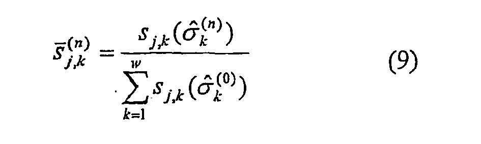


- Since conductivity is inversely related to voltage, the conductivity updating also can be based on an approximation of the inverse relation (Eq.13 based on 1+x ≈ 1/(1-x) at x<1), which can improve the convergence speed for both positive and negative changes in conductivity.

- Noting the validating condition Δσ<<σ, the


where the


- The procedure of multi-step iteration is performed as follows.
- (1) Pre-compute the assumed boundary voltage vector and the sensitivity matrix,

- (2) Measure the boundary voltage profiles and produce the relative change vector,


- (3) Pre-set the iteration control factors for the minimum convergence error, εS , the maximum number of inverse steps, δS , and the maximum number of iterations, δ C , for the GCG.
- (4) Initiate the first estimations for the error function vector and the conductivity vector,


- (5) Normalise the sensitivity matrix (the iteration steps n is from 1 to δ S )

- (6) Solve the inverse problem using the GCG method and then update the relative change in the conductivity vector (Maximum Iteration = δ C ),

- (7) Update the conductivity vector,

- (8) Solve the forward problem using the ordinary CG method to update the boundary voltage vector and sensitivity matrix,

- (9) Update the error vector,

- (10) Check the control factors to determine whether one of them has been reached,

- (11) If the convergence or the number of maximum iterations is not reached, the process jumps to step (5) until one of these conditions is reached. To summarise the procedure, its flowchart is given as
Figure 17 . - The sensitivity coefficient back-projection approximation method (SBP), utilising a normalised transpose matrix of the sensitivity matrix obtained from Eq.5 as a weighting matrix, was first refined for ERT by Kotre [Kotre, Physiology Measurements, 15, Supp. 2A 1992]. The approximation has been successfully applied to many industrial applications [Williams et al, Process tomography-principles, techniques and applications, Butterworth-Heinemann Ltd., 1995] due to its good anti-noise capability and fast solution speed. The physical definition may follow the basic principle of linear back projection: the relative change of the boundary voltage measurements is linearly back-projected to each pixel between two equipotential lines in the case of the equipotential back projection [Baber et al, Applied potential tomography', J. Phys. E: Sci. Instrum., 17,1984], or over whole domain in the case of the SBP [Kotre, Physiology Measurements, 15, Suppl. 2A 1992]. The sum of the products of the relative change and the weight factor/sensitivity coefficient at each pixel, normalised by the sum of their weight factors/sensitivity coefficients that are derived from all possible boundary measurements, approximately presents the relative change of the conductivity at this pixel.
- To investigate the accuracy and the limitation of the multi-step solution, a sequence of images were reconstructed from simulated data. A part of these results are presented in this patent. Only the adjacent sensing strategy [Brown et al, Proc. IEE Int. Conf on Electric and Magnetic field in Med. And Bio., 1985] was employed in these simulations. All references were taken from a homogeneous set-up with a conductivity of 0.11mS/cm. Meshes with 104 and 224 triangle pixels were used for simulating boundary voltages from these conductivity set-ups. To investigate the discretization error and mesh adaptability of the algorithm, some images were reconstructed using the mesh with 224 elements for data simulated using the mesh with 104 element. Electrode positions at the 224 element mesh also has an 11.25° anticlockwise rotation compared to those in the simulated set-ups with 104 element mesh.
- Considering the importance of the SBP in current applications, these simulated data were also reconstructed using the SBP. A mesh with 316 square pixels was employed for the SBP algorithm. The electrode position at the square mesh has an 11.25° anticlockwise rotation compared to those in the simulated set-ups with the 104 element mesh.
- To assess the imaging capability of the SCG algorithm, a Newton-Raphson method based algorithm with Tikhonov regularisation [Vaukonen, Scientific Abstracts of 2nd EPSRC Engineering Network Meeting, UCL, London, 2000], named as EIDORS (BIT and Diffuse Optical Tomography Reconstruction Software, UMIST 2000), is introduced to reconstruct a part of these data. These images are reconstructed using a mesh with 492 elements and parameters of the simulated contact impedance=0.005Ω/cm, Tikhonov regularization parameter=0.001 and the iteration number=6. The electrode position also has a clockwise rotation compared to the simulation set-up. The original simulated data are directly used for reconstructing images with the EIDORS. However, the data obtained from real measurements have to be regularised by applying the products of relative changes and the standard boundary voltages from a homogeneous set-up in the EIDORS.
- A set-up with a complex conductivity distribution, as shown in
Fig.18a , is reconstructed asFigs. 18b and 18c from the SBP and EIDORS algorithms respectively. It is obvious that the SBP algorithm could not deliver an accurate image for this set-up (Fig. 18b ). Both the EIDORS (Fig.18c ) and SCG (Fig.18d & f ) can reconstruct the complexity of the set-up. The image obtained from five steps of the SCG solution (Fig.18c ) provides a conductivity error of 3.32% and a boundary voltage error of 0.055%. The discretisation error caused by applying different mesh is reflected inFig.3f . - Imaging distinguishability of these algorithms was investigated and the results are given in
Fig.19 . Two 'objects' were located along a radius of a mesh (Fig.19a ). For the set-up, SBP can image the presence of the two objects but could not distinguish them (Fig.19b ). The edge of the objects' image is also merged with the boundary. The image obtained from EIDORS (Fig. 19c ) gives a better presentation about the object location with a clear separation from the boundary but is incapable of distinguishing between the two objects. SCG can clearly distinguish between the two objects although a certain artificial background noise presents (Fig.19d & f ). - Increasing the number of steps to solve the non-linear problem may improve the imaging accuracy. However, the most significant contribution is from the first step, which has already been shown in previous convergence graphs. Therefore, in practice, a single step solution would be widely acceptable for the balance of the imaging accuracy and speed.
- The single step method solution is be further simplified by obtaining an approximation of the inverse of
s (s is the normalised sensitivity matrix) and therefore the whole computation for reconstructing a single image only involves a multiplication of a matrix and a vector. The detailed information is provided as following. - The inverse solution can be denoted by equation (15) in a matrix form

- Where
s is the normalized sensitivity matrix, γ the conductivity relative change vector, and e the boundary relative change vector. - Since
s is neither square nor positively definite, direct solution to equation (15) using CG method would not exist. In order to be solved, equation (15) has to be transformed to equation (16) by applying minimization to equation (15).
- With
s Ts presenting a very large condition number, equation (16) cannot be solved using direct inverse method aiming to an accurate solution. An iterative method with finite steps gives equation (16) an approximation solution, which serves as a kind of regularization. Although being able to provide a sensible solution to equation (16), iterative methods involves much larger computation load than direct inverse methods by which an inverse matrix fors Ts can be obtained, and the solution to equation (16) only involves a multiplication of a matrix (s Ts )-1 ·s T with an vector e. - A method of obtaining (
s Ts )-1 using CG method and therefore providing a one-step solution to equation (16) is presented, having the advantages of both lower computation load and a sensible solution. - To simplify notations, let A= (
s Ts )-1, and form n equations in (17).
- Solving equations (17) using CG method with finite steps (typically 20), we can get vectors, x1, x2, x3 .....xn, which can be assembled into [xl, x2, .....xn], an approximation of (
s Ts ) -1. - Knowing
s , (s Ts )-1 ·s T can be pre-calculated and therefore equation (16) can be solved in one step. Let Γ*=(s Ts ) -1 ·s T , then the reconstruction process can be denoted as:
- Multiphase flow exists in many industrial processes. The phase distribution and interfaces in a multiphase flow carries significant information about the processes [Chhabra et al, Non-newtonian flow in the process industries - fundamentals and engineering applications, Butterworth-Heinemann, Oxford, 1999]. However its behaviour is extremely complex, which presents a great challenge to the study of the flow mechanisms and the measurement of multiphase flow. Both single modality and multi-modality imaging have been reported [Dyakowski et al, Powder Technol. 104, 1999; Hoyle et al, Proc. 1st World Congress on Industrial Process Tomography, Buxton, UK, 1999] as a means to identify flow regimes in two-phase flow. A direct imaging method for characterising gas-water flow based on a simple 4-electrode technique was proposed [Seleghim et al, Meas. Sci. Technol. 9 1998]. Solid concentration distribution can be imaged using electrical resistance tomography (ERT) and its local velocity profile could be interpreted by applying cross-correlation method for a twin-plane sensing system in a full-filled pipe flow [Lucas et al, Journal of Flow Measurement and Instrumentation, 10, 4,1999]. However, most previous flow applications using conventional electrical resistance tomography were only applied for vertical pipes or horizontal pipes in the absence of large gas bubbles. Signal saturation will occur for a half-filled pipe flow, such as churn flow in a horizontal flow loop, since part of electrodes lose their electrical contacts with the electrically conductive fluid. Imaging methods based on the electrical conductive ring sensing strategy has been used for measuring the two-phase flow with 'electrically continuous' and 'discontinuous' phases. As a preliminary test, several examples of identifying flow regimes using this technique are presented
- A.20 m flow loop (inner diameter, 50mm) fitted with ERT sensors was employed for the experiments. A schematic diagram and overview of the flow loop are given in
Figure 20 . Mains tap-water (conductivity = 0.304mS/cm) was used as the liquid phase and air, were introduced into the flow loop from a mixing jet-pump. Measurements were performed at ambient temperature. By controlling the air flowrate at the air inlet of the jet-pump, different flow regimes were generated in the low part of the flow loop. - The experiments were performed under different air flow-rates of 0.5m3/h, 1.5m3/h, 2.5m3/h, 3.5m3/h and the one less than 0.5m3/h in regard to the productions of slug flow, slug-churn flow, churn flow and bubbly flow regimes. The water flows were scaled with an accumulating tank during the experiments to get water flow rate and mean velocity. At the mean time, a number of photographs were recorded as visual presentations of these different flow regimes.
- Two-dimensional (2D) slice images were sequentially reconstructed. Some reconstructed images in respect to typical air cavities in the flow loop are shown in
Figure 21 , where the blue areas represent the air cavities or low conductivity regions and the red areas represent the water or high conductivity regions. - As an interesting test, a human hand was scanned using an EIT system. A 14.8cm diameter vessel fitted with one 16-electrode ring sensor and filled with 5.16mS/cm brine was employed. The adjacent electrode sensing strategy was applied with a pair of 10mA@9.6kHz sinusoidal currents for the test. The image data was made up of 15 measurement data sets acquired as the hand moved along the axial direction of the phantom while the water volume was kept the same. The signal-to-noise-ratio (SNR, here is the repeatability of reference voltage) was checked, which was within a maximum error 0.5%. Fifteen 2D images were reconstructed with the SCG [
Figure 22 ]. These fifteen 2D SCG images were further interpolated to a 3D hand image. A cutting value of 3.3mS/cm was applied to extract the surface of the hand skin as an iso-surface using Spyglass v1.00. An outline of the human hand has been successfully extracted as shown inFigure 23 . Some distortions can also be found, which may be caused by the electrode noise, the unstable position of the hand during the scanning and the 3-D effect of electrical field.
Claims (9)
- A method of measuring the distribution of electrical impedance of a multi-phase fluid, the method comprisingapplying between two of a plurality of metallic contacts, sequentially, an input electrical signal, which while applied to a pair of contacts, causes respective output signals to be generated between any other pair of contacts,and measuring said output electrical signals between successive pairs of contacts,
characterised in thatthe method comprises measuring the distribution of the electrical impedance using an electrically conductive ring electrode (1) surrounding the fluid and having an electrical conductivity higher than that of the fluid, the ring electrode (1) being cylindrical, and the plurality of metallic contacts (2) being spatially distributed around the axis of the ring and being embedded into the conductive ring in good electric contact with an outside wall of the ring or penetrated through the wall of the ring electrode in good electrical contact with the wall,
whereby the contacts of each pair of contacts selected for signal generation and for signal reception, respectively, span an azimuthal angle of about π/2 with respect to the axis of the conductive ring electrode (1). - The method according to Claim 1 characterised in that the electrically conductive ring is made of solid substances selected from metal, conductive rubber, ceramics, or a combination of the aforesaid.
- The method according to any of the preceding claims characterised in that a target having a measurable distribution of electrical impedance is selected from process fluid and a part of a human body.
- The method according to Claim 1 characterised in that a conductive disk is used to construct said electrode, with a PCB as its connection.
- The method according to Claim 1 characterised in that said conductive electrode is made in micro-scale.
- The method according to Claim 5 characterised in that the micro-scale conductive electrode is made on silicon chips.
- The method according to Claim 5 characterised in that the micro-scale conductive electrode is integrated with a measurement and processing circuit.

- An apparatus for measuring the distribution of electrical impedance of a multi-phase fluid, the apparatus being arranged toapply between two of a plurality of metallic contacts, sequentially, an input electrical signal, which while applied to a pair of the contacts, causes respective output singals to be generated between any other pair of contacts, and measure said output electrical signals between successive pairs of contacts, characterised in thatthe apparatus is arranged to measure the distribution of the electrical impedance using a cylindrical electrically conductive ring electrode (1) surrounding the fluid, the plurality of metallic contacts (2) being spatially distributed around the axis of the ring and embedded into the conductive ring in good electric contact with an outside wall of the ring or penetrated through the wall of the ring electrode in good electrical contact with said wall, whereby the contacts of each pair of contacts selected for signal generation and for signal reception, respectively, span an azimuthal angle of substantially π/2 with respect to the axis of the conductive ring electrode (1).
- A method of determining the internal structure of a body which utilises a method according to Claim 1.
Applications Claiming Priority (5)
| Application Number | Priority Date | Filing Date | Title |
|---|---|---|---|
| GB0031854 | 2000-12-30 | ||
| GB0031854A GB0031854D0 (en) | 2000-12-30 | 2000-12-30 | Electrical impedance tomography for flow measurement |
| GB0120772A GB0120772D0 (en) | 2001-08-25 | 2001-08-25 | Electrical impedance tompgraphy for flow measurement |
| GB0120772 | 2001-08-25 | ||
| PCT/GB2001/005636 WO2002053029A1 (en) | 2000-12-30 | 2001-12-28 | Electrical impedance tomography |
Publications (2)
| Publication Number | Publication Date |
|---|---|
| EP1347706A1 EP1347706A1 (en) | 2003-10-01 |
| EP1347706B1 true EP1347706B1 (en) | 2008-05-21 |
Family
ID=26245509
Family Applications (1)
| Application Number | Title | Priority Date | Filing Date |
|---|---|---|---|
| EP01272705A Expired - Lifetime EP1347706B1 (en) | 2000-12-30 | 2001-12-28 | Electrical impedance tomography |
Country Status (6)
| Country | Link |
|---|---|
| US (1) | US6940286B2 (en) |
| EP (1) | EP1347706B1 (en) |
| AT (1) | ATE395866T1 (en) |
| CA (1) | CA2472220A1 (en) |
| DE (1) | DE60134173D1 (en) |
| WO (1) | WO2002053029A1 (en) |
Families Citing this family (82)
| Publication number | Priority date | Publication date | Assignee | Title |
|---|---|---|---|---|
| DE10238824A1 (en) * | 2002-08-23 | 2004-03-11 | Forschungszentrum Jülich GmbH | Method and device for the rapid tomographic measurement of the electrical conductivity distribution in a sample |
| AU2003900857A0 (en) | 2003-02-26 | 2003-03-13 | Commonwealth Scientific And Industrial Research Organisation | Method and apparatus for characterising multiphase fluid mixtures |
| US8532735B2 (en) * | 2003-04-15 | 2013-09-10 | Koninklijke Philips N.V. | Device and method for examination and use of an electrical field in an object under examination containing magnetic particles |
| US20050243087A1 (en) * | 2004-04-30 | 2005-11-03 | Shmuel Aharon | GPU-based Finite Element |
| US7701227B2 (en) * | 2005-01-05 | 2010-04-20 | Rensselaer Polytechnic Institute | High precision voltage source for electrical impedance tomography |
| EP1846893B1 (en) * | 2005-02-03 | 2015-09-16 | Koninklijke Philips N.V. | Radial adaptive filter for metal artifact correction |
| AU2006265761B2 (en) | 2005-07-01 | 2011-08-11 | Impedimed Limited | Monitoring system |
| CA2609111C (en) | 2005-07-01 | 2016-10-18 | Scott Chetham | A method and apparatus for performing impedance measurements in accordance with determining an electrode arrangement using a displayed representation |
| US20100292603A1 (en) * | 2005-09-21 | 2010-11-18 | Beth Israel Deaconess Medical Center, Inc. | Electrical Impedance Myography |
| ES2476999T3 (en) | 2005-10-11 | 2014-07-15 | Impedimed Limited | Hydration Status Monitoring |
| CN100362341C (en) * | 2005-12-22 | 2008-01-16 | 天津大学 | ERT/ECT Dual Mode Imaging System Composite Array Sensor |
| EP1984723B1 (en) | 2006-02-01 | 2019-05-15 | Ecole Polytechnique Federale de Lausanne (EPFL) | Impedance measurement device for characterizing particles in a micro channel |
| CN100401044C (en) * | 2006-03-21 | 2008-07-09 | 天津大学 | Dual-mode electrical imaging system sensor and image reconstruction method based on the sensor |
| NO324812B1 (en) * | 2006-05-05 | 2007-12-10 | Multi Phase Meters As | Method and apparatus for tomographic multiphase flow measurements |
| CN100549684C (en) * | 2007-04-18 | 2009-10-14 | 天津大学 | Image reconstruction method based on square dual-mode self-calibration sensor |
| CA2684324C (en) | 2007-04-20 | 2017-05-30 | Impedimed Limited | Monitoring system and probe |
| WO2009018620A1 (en) | 2007-08-09 | 2009-02-12 | Impedimed Limited | Impedance measurement process |
| US8102182B2 (en) * | 2007-10-11 | 2012-01-24 | University Of Utah Research Foundation | Systems and methods for measuring the electrical properties of a microparticle |
| US8386010B2 (en) * | 2008-10-23 | 2013-02-26 | Covidien Lp | Surgical tissue monitoring system |
| SE533704C2 (en) | 2008-12-05 | 2010-12-07 | Flatfrog Lab Ab | Touch sensitive apparatus and method for operating the same |
| FI123318B (en) * | 2009-09-29 | 2013-02-28 | Outotec Oyj | Three-dimensional imaging of a mass flow |
| JP5643829B2 (en) | 2009-10-26 | 2014-12-17 | インぺディメッド リミテッドImpedimed Limited | Method and apparatus for use in impedance measurement analysis |
| AU2010321683B2 (en) | 2009-11-18 | 2014-06-26 | Impedimed Limited | Signal distribution for patient-electrode measurements |
| US8121804B2 (en) * | 2010-01-05 | 2012-02-21 | General Electric Company | Electrical network analysis of a multiphase system |
| US8536883B2 (en) | 2010-04-29 | 2013-09-17 | Schlumberger Technology Corporation | Method of measuring a multiphase flow |
| TW201203052A (en) | 2010-05-03 | 2012-01-16 | Flatfrog Lab Ab | Touch determination by tomographic reconstruction |
| US8054094B1 (en) * | 2010-06-10 | 2011-11-08 | General Electric Company | Image reconstruction based constrained maximization |
| US8508238B2 (en) | 2010-08-12 | 2013-08-13 | General Electric Company | System and method for performing electrical impedance tomography |
| FI123789B (en) * | 2010-11-30 | 2013-10-31 | Metso Automation Oy | Measurement of the amount of solid in a suspension |
| CN102274025B (en) * | 2011-05-30 | 2012-11-28 | 郑州大学 | Multi-electrode electrical impedance tomography data acquisition system |
| US8892379B2 (en) | 2011-06-30 | 2014-11-18 | General Electric Company | System and method for soft-field reconstruction |
| US9989453B2 (en) * | 2011-08-23 | 2018-06-05 | Cidra Corporate Services, Inc. | Tomographic determination of scale build-up in pipes and other tanks, cells, vessels or containers |
| US8963562B2 (en) | 2011-08-31 | 2015-02-24 | General Electric Company | Transducer configurations and methods for transducer positioning in electrical impedance tomography |
| EP2786132A1 (en) * | 2011-11-30 | 2014-10-08 | General Electric Company | High-side current measurement technique for multi-phase fluid |
| US8700121B2 (en) | 2011-12-14 | 2014-04-15 | Intersection Medical, Inc. | Devices for determining the relative spatial change in subsurface resistivities across frequencies in tissue |
| US10168835B2 (en) | 2012-05-23 | 2019-01-01 | Flatfrog Laboratories Ab | Spatial resolution in touch displays |
| CN103018284B (en) * | 2012-12-14 | 2015-05-13 | 北京航空航天大学 | Four-terminal electrical impedance tomography method based on two-terminal impedance measurement mode |
| US10019113B2 (en) | 2013-04-11 | 2018-07-10 | Flatfrog Laboratories Ab | Tomographic processing for touch detection |
| US9874978B2 (en) | 2013-07-12 | 2018-01-23 | Flatfrog Laboratories Ab | Partial detect mode |
| CN103604993B (en) * | 2013-09-12 | 2017-01-04 | 陕西航天导航设备有限公司 | Electric installation dynamic contact resistance test equipment and method of testing |
| US10126882B2 (en) | 2014-01-16 | 2018-11-13 | Flatfrog Laboratories Ab | TIR-based optical touch systems of projection-type |
| WO2015108479A1 (en) | 2014-01-16 | 2015-07-23 | Flatfrog Laboratories Ab | Light coupling in tir-based optical touch systems |
| JP6423183B2 (en) * | 2014-06-25 | 2018-11-14 | 株式会社Ihi | Tomography measurement method |
| US10161886B2 (en) | 2014-06-27 | 2018-12-25 | Flatfrog Laboratories Ab | Detection of surface contamination |
| GB201416287D0 (en) | 2014-09-15 | 2014-10-29 | Univ Leeds | Tomography apparatus, multi-phase flow monitoring system and corresponding methods |
| GB201416280D0 (en) | 2014-09-15 | 2014-10-29 | Univ Leeds | Tomography apparatus and method |
| CN107209608A (en) | 2015-01-28 | 2017-09-26 | 平蛙实验室股份公司 | Dynamic Touch Isolation Frame |
| US10318074B2 (en) | 2015-01-30 | 2019-06-11 | Flatfrog Laboratories Ab | Touch-sensing OLED display with tilted emitters |
| EP3256936A4 (en) | 2015-02-09 | 2018-10-17 | FlatFrog Laboratories AB | Optical touch system comprising means for projecting and detecting light beams above and inside a transmissive panel |
| WO2016140612A1 (en) | 2015-03-02 | 2016-09-09 | Flatfrog Laboratories Ab | Optical component for light coupling |
| US10775937B2 (en) | 2015-12-09 | 2020-09-15 | Flatfrog Laboratories Ab | Stylus identification |
| US10781687B2 (en) | 2015-12-16 | 2020-09-22 | Halliburton Energy Services, Inc. | Electrical impedance tomography using a switchable array |
| CN105675658A (en) * | 2016-01-13 | 2016-06-15 | 天津大学 | Electrical resistance tomography sensor with built-in conductor ring |
| GB2546522B (en) | 2016-01-21 | 2020-02-12 | Atout Process Ltd | Method and apparatus for measuring flows |
| CN105954351B (en) * | 2016-04-11 | 2019-03-26 | 中国石油大学(华东) | Based on electromagnetism-acoustical coupling oil-water two-phase flow process tomographic imaging method |
| DE102016114611A1 (en) | 2016-08-07 | 2018-02-08 | Karl-Heinz Fromm | Electrode arrangement, in particular for the electrical impedance tomography |
| DE102016223029A1 (en) | 2016-11-22 | 2018-05-24 | Leibniz-Institut Für Festkörper-Und Werkstoffforschung Dresden E.V. | THREE-DIMENSIONAL TOMOGRAPH |
| CN110100226A (en) | 2016-11-24 | 2019-08-06 | 平蛙实验室股份公司 | The Automatic Optimal of touch signal |
| EP3667475B1 (en) | 2016-12-07 | 2022-09-07 | FlatFrog Laboratories AB | A curved touch device |
| CN116679845A (en) | 2017-02-06 | 2023-09-01 | 平蛙实验室股份公司 | touch sensing device |
| WO2018174786A1 (en) | 2017-03-22 | 2018-09-27 | Flatfrog Laboratories | Pen differentiation for touch displays |
| WO2018182476A1 (en) | 2017-03-28 | 2018-10-04 | Flatfrog Laboratories Ab | Touch sensing apparatus and method for assembly |
| EP3676694A4 (en) | 2017-09-01 | 2021-06-09 | FlatFrog Laboratories AB | Improved optical component |
| US11567610B2 (en) | 2018-03-05 | 2023-01-31 | Flatfrog Laboratories Ab | Detection line broadening |
| WO2020080992A1 (en) | 2018-10-20 | 2020-04-23 | Flatfrog Laboratories Ab | Frame for a touch-sensitive device and tool therefor |
| KR102241035B1 (en) * | 2018-11-16 | 2021-04-16 | 경희대학교 산학협력단 | Screening apparatus using multi-channel array electrode probe and operating method thereof |
| WO2020113157A1 (en) * | 2018-11-28 | 2020-06-04 | Northwestern University | High resolution two-dimensional resistance tomography |
| WO2020153890A1 (en) | 2019-01-25 | 2020-07-30 | Flatfrog Laboratories Ab | A videoconferencing terminal and method of operating the same |
| EP3698713B1 (en) | 2019-02-20 | 2023-09-06 | Löwenstein Medical Technology S.A. | System for detecting a patient's respiratory effort |
| US12056316B2 (en) | 2019-11-25 | 2024-08-06 | Flatfrog Laboratories Ab | Touch-sensing apparatus |
| DE102020100980A1 (en) | 2020-01-16 | 2021-07-22 | Endress+Hauser SE+Co. KG | Method for determining and / or monitoring at least one property of a medium |
| EP4100822A4 (en) | 2020-02-08 | 2024-02-28 | FlatFrog Laboratories AB | TOUCH DEVICE WITH LOW LATENCY INTERACTIONS |
| CN121614054A (en) | 2020-02-10 | 2026-03-06 | 平蛙实验室股份公司 | Touch sensing apparatus and method of manufacturing frame element of touch sensing apparatus |
| US11536676B2 (en) | 2020-10-02 | 2022-12-27 | Triad National Security, Llc | Characterization of fluid inside pipe using multi frequency electrical signal |
| CN113724349B (en) * | 2021-07-30 | 2025-05-30 | 神华上航疏浚有限责任公司 | Method, device, computer equipment and storage medium for calculating flow velocity in horizontal pipeline |
| US11754520B2 (en) * | 2021-08-26 | 2023-09-12 | Beihang University | Dynamic impedance imaging system |
| CN113945609B (en) * | 2021-10-13 | 2024-03-19 | 中国人民解放军国防科技大学 | An ERT sensor for high-speed rail contact line wear detection |
| CN114062435A (en) * | 2021-10-21 | 2022-02-18 | 北京工业大学 | Flexible sensor with sensitivity correction function based on electrical impedance imaging principle |
| CN114216933B (en) * | 2021-12-16 | 2023-11-24 | 北京航空航天大学 | Gas-liquid two-phase flow measuring device and method suitable for open-area flow field |
| KR20240083312A (en) * | 2022-12-05 | 2024-06-12 | 현대자동차주식회사 | System of diagnosing mixture of dry electrode |
| CN116400150A (en) * | 2023-03-13 | 2023-07-07 | 中国海洋石油集团有限公司 | Non-contact saturated field measurement system |
| FR3152593B1 (en) * | 2023-09-06 | 2025-09-26 | Commissariat Energie Atomique | System for reducing or optimizing the consumption or electrical production of fluidic equipment with at least one rotating component. |
Family Cites Families (9)
| Publication number | Priority date | Publication date | Assignee | Title |
|---|---|---|---|---|
| DE2813068A1 (en) | 1978-03-25 | 1979-10-04 | Philips Patentverwaltung | METHOD AND DEVICE FOR DETERMINING INTERNAL BODY STRUCTURES |
| IL62861A (en) | 1981-05-13 | 1988-01-31 | Yeda Res & Dev | Method and apparatus for carrying out electric tomography |
| US4617939A (en) | 1982-04-30 | 1986-10-21 | The University Of Sheffield | Tomography |
| GB2119520B (en) | 1982-04-30 | 1985-05-15 | Brian Hilton Brown | Tomography |
| GB8415236D0 (en) | 1984-06-14 | 1984-07-18 | Univ Sheffield | Tomography |
| US4920490A (en) | 1988-01-28 | 1990-04-24 | Rensselaer Polytechnic Institute | Process and apparatus for distinguishing conductivities by electric current computed tomography |
| US5272624A (en) | 1990-10-02 | 1993-12-21 | Rensselaer Polytechnic Institute | Current patterns for impedance tomography |
| DE69505799T2 (en) | 1994-03-11 | 1999-04-22 | British Technology Group Ltd., London | ELECTRICAL IMPEDANCE TOMOGRAPHY |
| CA2191285A1 (en) * | 1996-11-26 | 1998-05-26 | Philip Maurice Church | Electrode arrangement for electrical impedance tomography system |
-
2001
- 2001-12-28 EP EP01272705A patent/EP1347706B1/en not_active Expired - Lifetime
- 2001-12-28 CA CA002472220A patent/CA2472220A1/en not_active Abandoned
- 2001-12-28 WO PCT/GB2001/005636 patent/WO2002053029A1/en not_active Ceased
- 2001-12-28 US US10/250,327 patent/US6940286B2/en not_active Expired - Lifetime
- 2001-12-28 DE DE60134173T patent/DE60134173D1/en not_active Expired - Lifetime
- 2001-12-28 AT AT01272705T patent/ATE395866T1/en not_active IP Right Cessation
Also Published As
| Publication number | Publication date |
|---|---|
| EP1347706A1 (en) | 2003-10-01 |
| DE60134173D1 (en) | 2008-07-03 |
| CA2472220A1 (en) | 2002-07-11 |
| ATE395866T1 (en) | 2008-06-15 |
| US6940286B2 (en) | 2005-09-06 |
| WO2002053029A1 (en) | 2002-07-11 |
| US20040130338A1 (en) | 2004-07-08 |
Similar Documents
| Publication | Publication Date | Title |
|---|---|---|
| US6940286B2 (en) | Electrical impedance tomography | |
| EP2483672B1 (en) | Three dimensional imaging of a mass flow | |
| Ceccio et al. | A review of electrical impedance techniques for the measurement of multiphase flows | |
| Borsic | Regularisation methods for imaging from electrical measurements | |
| US8614707B2 (en) | 3D and real time electrical capacitance volume-tomography sensor design and image reconstruction | |
| EP2343539B1 (en) | Electrical network representation of a distributed system | |
| CN109690260B (en) | Displacement Current Phase Tomography for Lossy Media Imaging | |
| Heikkinen et al. | Real time three-dimensional electrical impedance tomography applied in multiphase flow imaging | |
| Ma et al. | Application of electrical resistance tomography system to monitor gas/liquid two-phase flow in a horizontal pipe | |
| JP5739731B2 (en) | Image reconstruction based on constrained maximization | |
| CN105308445A (en) | Method and apparatus for investigating permittivity in a target domain | |
| Wang et al. | A highly adaptive electrical impedance sensing system for flow measurement | |
| CN101794453B (en) | Reconstruction method of node mapping image based on regression analysis | |
| Kim et al. | Image reconstruction using voltage–current system in electrical impedance tomography | |
| Arif et al. | Joint reconstruction of conductivity and velocity in two-phase flows using electromagnetic flow tomography and electrical tomography: A simulation study | |
| Alme et al. | Comparison of different measurement protocols in electrical capacitance tomography using simulations | |
| CN102540276B (en) | Soft field tomography system and method | |
| Jiang et al. | Contactless electrical impedance and ultrasonic tomography: Correlation, comparison and complementarity study | |
| Hadinia et al. | An element-free Galerkin forward solver for the complete-electrode model in electrical impedance tomography | |
| Heikkinen et al. | Electrical process tomography with known internal structures and resistivities | |
| Song et al. | An image reconstruction framework based on boundary voltages for ultrasound modulated electrical impedance tomography | |
| Ru et al. | Neural networks in electrical capacitance tomography (ECT)-based interface detection | |
| Steiner et al. | A sequential ultrasound and electrical capacitance process tomography system | |
| Tereshko | Numerical analysis of inverse problems for electric field measurements | |
| Baumeister | Identification of Parameters, Ill-Posedness |
Legal Events
| Date | Code | Title | Description |
|---|---|---|---|
| PUAI | Public reference made under article 153(3) epc to a published international application that has entered the european phase |
Free format text: ORIGINAL CODE: 0009012 |
|
| 17P | Request for examination filed |
Effective date: 20030728 |
|
| AK | Designated contracting states |
Kind code of ref document: A1 Designated state(s): AT BE CH CY DE DK ES FI FR GB GR IE IT LI LU MC NL PT SE TR |
|
| AX | Request for extension of the european patent |
Extension state: AL LT LV MK RO SI |
|
| 17Q | First examination report despatched |
Effective date: 20050831 |
|
| GRAP | Despatch of communication of intention to grant a patent |
Free format text: ORIGINAL CODE: EPIDOSNIGR1 |
|
| GRAS | Grant fee paid |
Free format text: ORIGINAL CODE: EPIDOSNIGR3 |
|
| GRAA | (expected) grant |
Free format text: ORIGINAL CODE: 0009210 |
|
| AK | Designated contracting states |
Kind code of ref document: B1 Designated state(s): AT BE CH CY DE DK ES FI FR GB GR IE IT LI LU MC NL PT SE TR |
|
| REG | Reference to a national code |
Ref country code: GB Ref legal event code: FG4D |
|
| REG | Reference to a national code |
Ref country code: CH Ref legal event code: EP |
|
| REF | Corresponds to: |
Ref document number: 60134173 Country of ref document: DE Date of ref document: 20080703 Kind code of ref document: P |
|
| REG | Reference to a national code |
Ref country code: IE Ref legal event code: FG4D |
|
| REG | Reference to a national code |
Ref country code: CH Ref legal event code: NV Representative=s name: TROESCH SCHEIDEGGER WERNER AG |
|
| PG25 | Lapsed in a contracting state [announced via postgrant information from national office to epo] |
Ref country code: FI Free format text: LAPSE BECAUSE OF FAILURE TO SUBMIT A TRANSLATION OF THE DESCRIPTION OR TO PAY THE FEE WITHIN THE PRESCRIBED TIME-LIMIT Effective date: 20080521 Ref country code: ES Free format text: LAPSE BECAUSE OF FAILURE TO SUBMIT A TRANSLATION OF THE DESCRIPTION OR TO PAY THE FEE WITHIN THE PRESCRIBED TIME-LIMIT Effective date: 20080901 |
|
| PG25 | Lapsed in a contracting state [announced via postgrant information from national office to epo] |
Ref country code: AT Free format text: LAPSE BECAUSE OF FAILURE TO SUBMIT A TRANSLATION OF THE DESCRIPTION OR TO PAY THE FEE WITHIN THE PRESCRIBED TIME-LIMIT Effective date: 20080521 |
|
| PG25 | Lapsed in a contracting state [announced via postgrant information from national office to epo] |
Ref country code: SE Free format text: LAPSE BECAUSE OF FAILURE TO SUBMIT A TRANSLATION OF THE DESCRIPTION OR TO PAY THE FEE WITHIN THE PRESCRIBED TIME-LIMIT Effective date: 20080821 Ref country code: PT Free format text: LAPSE BECAUSE OF FAILURE TO SUBMIT A TRANSLATION OF THE DESCRIPTION OR TO PAY THE FEE WITHIN THE PRESCRIBED TIME-LIMIT Effective date: 20081021 Ref country code: DK Free format text: LAPSE BECAUSE OF FAILURE TO SUBMIT A TRANSLATION OF THE DESCRIPTION OR TO PAY THE FEE WITHIN THE PRESCRIBED TIME-LIMIT Effective date: 20080521 |
|
| PG25 | Lapsed in a contracting state [announced via postgrant information from national office to epo] |
Ref country code: BE Free format text: LAPSE BECAUSE OF FAILURE TO SUBMIT A TRANSLATION OF THE DESCRIPTION OR TO PAY THE FEE WITHIN THE PRESCRIBED TIME-LIMIT Effective date: 20080521 |
|
| PLBE | No opposition filed within time limit |
Free format text: ORIGINAL CODE: 0009261 |
|
| STAA | Information on the status of an ep patent application or granted ep patent |
Free format text: STATUS: NO OPPOSITION FILED WITHIN TIME LIMIT |
|
| 26N | No opposition filed |
Effective date: 20090224 |
|
| PG25 | Lapsed in a contracting state [announced via postgrant information from national office to epo] |
Ref country code: MC Free format text: LAPSE BECAUSE OF NON-PAYMENT OF DUE FEES Effective date: 20081231 |
|
| PG25 | Lapsed in a contracting state [announced via postgrant information from national office to epo] |
Ref country code: IE Free format text: LAPSE BECAUSE OF NON-PAYMENT OF DUE FEES Effective date: 20081228 |
|
| PG25 | Lapsed in a contracting state [announced via postgrant information from national office to epo] |
Ref country code: LU Free format text: LAPSE BECAUSE OF NON-PAYMENT OF DUE FEES Effective date: 20081228 Ref country code: CY Free format text: LAPSE BECAUSE OF FAILURE TO SUBMIT A TRANSLATION OF THE DESCRIPTION OR TO PAY THE FEE WITHIN THE PRESCRIBED TIME-LIMIT Effective date: 20080521 |
|
| PG25 | Lapsed in a contracting state [announced via postgrant information from national office to epo] |
Ref country code: TR Free format text: LAPSE BECAUSE OF FAILURE TO SUBMIT A TRANSLATION OF THE DESCRIPTION OR TO PAY THE FEE WITHIN THE PRESCRIBED TIME-LIMIT Effective date: 20080521 |
|
| PG25 | Lapsed in a contracting state [announced via postgrant information from national office to epo] |
Ref country code: GR Free format text: LAPSE BECAUSE OF FAILURE TO SUBMIT A TRANSLATION OF THE DESCRIPTION OR TO PAY THE FEE WITHIN THE PRESCRIBED TIME-LIMIT Effective date: 20080822 |
|
| REG | Reference to a national code |
Ref country code: FR Ref legal event code: PLFP Year of fee payment: 15 |
|
| REG | Reference to a national code |
Ref country code: FR Ref legal event code: PLFP Year of fee payment: 16 |
|
| REG | Reference to a national code |
Ref country code: FR Ref legal event code: PLFP Year of fee payment: 17 |
|
| PGFP | Annual fee paid to national office [announced via postgrant information from national office to epo] |
Ref country code: IT Payment date: 20171228 Year of fee payment: 17 |
|
| PGFP | Annual fee paid to national office [announced via postgrant information from national office to epo] |
Ref country code: PL Payment date: 20180928 Year of fee payment: 9 |
|
| PGFP | Annual fee paid to national office [announced via postgrant information from national office to epo] |
Ref country code: FR Payment date: 20181219 Year of fee payment: 18 |
|
| PG25 | Lapsed in a contracting state [announced via postgrant information from national office to epo] |
Ref country code: IT Free format text: LAPSE BECAUSE OF NON-PAYMENT OF DUE FEES Effective date: 20181228 |
|
| PGFP | Annual fee paid to national office [announced via postgrant information from national office to epo] |
Ref country code: NL Payment date: 20191219 Year of fee payment: 19 |
|
| PGFP | Annual fee paid to national office [announced via postgrant information from national office to epo] |
Ref country code: CH Payment date: 20191219 Year of fee payment: 19 |
|
| PGFP | Annual fee paid to national office [announced via postgrant information from national office to epo] |
Ref country code: GB Payment date: 20191220 Year of fee payment: 19 |
|
| REG | Reference to a national code |
Ref country code: DE Ref legal event code: R119 Ref document number: 60134173 Country of ref document: DE |
|
| PG25 | Lapsed in a contracting state [announced via postgrant information from national office to epo] |
Ref country code: FR Free format text: LAPSE BECAUSE OF NON-PAYMENT OF DUE FEES Effective date: 20191231 Ref country code: DE Free format text: LAPSE BECAUSE OF NON-PAYMENT OF DUE FEES Effective date: 20200701 |
|
| REG | Reference to a national code |
Ref country code: CH Ref legal event code: PL |
|
| REG | Reference to a national code |
Ref country code: NL Ref legal event code: MM Effective date: 20210101 |
|
| GBPC | Gb: european patent ceased through non-payment of renewal fee |
Effective date: 20201228 |
|
| PG25 | Lapsed in a contracting state [announced via postgrant information from national office to epo] |
Ref country code: NL Free format text: LAPSE BECAUSE OF NON-PAYMENT OF DUE FEES Effective date: 20210101 |
|
| PG25 | Lapsed in a contracting state [announced via postgrant information from national office to epo] |
Ref country code: LI Free format text: LAPSE BECAUSE OF NON-PAYMENT OF DUE FEES Effective date: 20201231 Ref country code: CH Free format text: LAPSE BECAUSE OF NON-PAYMENT OF DUE FEES Effective date: 20201231 Ref country code: GB Free format text: LAPSE BECAUSE OF NON-PAYMENT OF DUE FEES Effective date: 20201228 |