EP1347670A1 - Material for organic electroluminescence device and its manufacturing method - Google Patents
Material for organic electroluminescence device and its manufacturing method Download PDFInfo
- Publication number
- EP1347670A1 EP1347670A1 EP01271789A EP01271789A EP1347670A1 EP 1347670 A1 EP1347670 A1 EP 1347670A1 EP 01271789 A EP01271789 A EP 01271789A EP 01271789 A EP01271789 A EP 01271789A EP 1347670 A1 EP1347670 A1 EP 1347670A1
- Authority
- EP
- European Patent Office
- Prior art keywords
- laser beam
- target
- emission center
- source
- process according
- Prior art date
- Legal status (The legal status is an assumption and is not a legal conclusion. Google has not performed a legal analysis and makes no representation as to the accuracy of the status listed.)
- Pending
Links
Images

Classifications
-
- H—ELECTRICITY
- H10—SEMICONDUCTOR DEVICES; ELECTRIC SOLID-STATE DEVICES NOT OTHERWISE PROVIDED FOR
- H10K—ORGANIC ELECTRIC SOLID-STATE DEVICES
- H10K71/00—Manufacture or treatment specially adapted for the organic devices covered by this subclass
- H10K71/10—Deposition of organic active material
- H10K71/16—Deposition of organic active material using physical vapour deposition [PVD], e.g. vacuum deposition or sputtering
- H10K71/162—Deposition of organic active material using physical vapour deposition [PVD], e.g. vacuum deposition or sputtering using laser ablation
-
- H—ELECTRICITY
- H05—ELECTRIC TECHNIQUES NOT OTHERWISE PROVIDED FOR
- H05B—ELECTRIC HEATING; ELECTRIC LIGHT SOURCES NOT OTHERWISE PROVIDED FOR; CIRCUIT ARRANGEMENTS FOR ELECTRIC LIGHT SOURCES, IN GENERAL
- H05B33/00—Electroluminescent light sources
- H05B33/10—Apparatus or processes specially adapted to the manufacture of electroluminescent light sources
-
- H—ELECTRICITY
- H10—SEMICONDUCTOR DEVICES; ELECTRIC SOLID-STATE DEVICES NOT OTHERWISE PROVIDED FOR
- H10K—ORGANIC ELECTRIC SOLID-STATE DEVICES
- H10K50/00—Organic light-emitting devices
- H10K50/10—OLEDs or polymer light-emitting diodes [PLED]
- H10K50/11—OLEDs or polymer light-emitting diodes [PLED] characterised by the electroluminescent [EL] layers
-
- H—ELECTRICITY
- H10—SEMICONDUCTOR DEVICES; ELECTRIC SOLID-STATE DEVICES NOT OTHERWISE PROVIDED FOR
- H10K—ORGANIC ELECTRIC SOLID-STATE DEVICES
- H10K50/00—Organic light-emitting devices
- H10K50/10—OLEDs or polymer light-emitting diodes [PLED]
- H10K50/11—OLEDs or polymer light-emitting diodes [PLED] characterised by the electroluminescent [EL] layers
- H10K50/125—OLEDs or polymer light-emitting diodes [PLED] characterised by the electroluminescent [EL] layers specially adapted for multicolour light emission, e.g. for emitting white light
-
- H—ELECTRICITY
- H10—SEMICONDUCTOR DEVICES; ELECTRIC SOLID-STATE DEVICES NOT OTHERWISE PROVIDED FOR
- H10K—ORGANIC ELECTRIC SOLID-STATE DEVICES
- H10K50/00—Organic light-emitting devices
- H10K50/10—OLEDs or polymer light-emitting diodes [PLED]
- H10K50/14—Carrier transporting layers
-
- H—ELECTRICITY
- H10—SEMICONDUCTOR DEVICES; ELECTRIC SOLID-STATE DEVICES NOT OTHERWISE PROVIDED FOR
- H10K—ORGANIC ELECTRIC SOLID-STATE DEVICES
- H10K85/00—Organic materials used in the body or electrodes of devices covered by this subclass
- H10K85/60—Organic compounds having low molecular weight
-
- H—ELECTRICITY
- H10—SEMICONDUCTOR DEVICES; ELECTRIC SOLID-STATE DEVICES NOT OTHERWISE PROVIDED FOR
- H10K—ORGANIC ELECTRIC SOLID-STATE DEVICES
- H10K85/00—Organic materials used in the body or electrodes of devices covered by this subclass
- H10K85/60—Organic compounds having low molecular weight
- H10K85/649—Aromatic compounds comprising a hetero atom
Definitions
- the present invention relates to a process for producing a material for an organic electroluminescent device by implanting or injecting an emission center-forming compound by molecular implantation with laser, a material for an organic electroluminescent device obtained by this process, and to an organic electroluminescent device (elements) produced with this organic electroluminescent device material.
- Electroluminescent devices (hereinafter, occasionally referred to simply as EL devices) have generally been classified as inorganic EL devices or organic EL devices according to the materials they are made from. Some inorganic EL devices utilizing inorganic fluorescent molecules are in practical use partly, and have been brought into application to the backlight of clocks or the like. Meanwhile, organic EL devices have been desired to be brought into practical use because of their being more excellent in high brightness or luminance, high efficiency, and high-speed response than inorganic ones.
- Electroluminescent devices are constituted of a compound or compounds having an electron-transporting function, a hole-transporting function, and an emission center-forming function.
- devices of the single-layer mode having a single layer provided with all the functions mentioned above, and those of the multilayer-mode composed of layers each having different functions.
- the principle of light emission is considered to be based on the phenomenon that electrons or holes injected from a pair of electrodes recombine within a light-emitting layer to form excitons, exciting the molecules of a light emissive material for the light-emitting layer.
- a low-molecular weight compound of high light-emission efficiency As a compound constituting each layer, a low-molecular weight compound of high light-emission efficiency, a macromolecular compound having a high physical strength, or the like is employed.
- a film is formed by means of a vapor deposition technique, while a macromolecular compound is formed into a film by coating or applying a solution in many cases.
- JP-A-8-96959 and JP-A-9-63770 disclose organic EL devices comprising a single light-emitting layer made of a polymer binder having both electron-transporting function and hole-transporting function, within which varieties of fluorescent dyes (or colorants, pigments) are dispersed. These organic EL devises are reported to present, as a whole, white light due to the light emission of each light-emitting compound independent of one another. Moreover, as compared with organic EL devices of the multilayer-mode, those of the single-layer mode are hardly deteriorated in light-emission intensity.
- Fine patterning, particularly multicolor patterning (full-coloration) of these organic EL devices is difficult because, in their fabrication, a film is formed by means of a solution coating technique in which a solution of a polymer binder and a fluorescent dye(s) dispersed in a specific solvent is applied onto a substrate.
- the color filter method or color-converting method has the advantage of not requiring the patterning of a light-emitting layer, but suffers deterioration in conversion efficiency caused by the use of a filter.
- a pattern formed by ink-jet printing shows a center-raised, i.e., conical profile and is inferior in smoothness of its surface, it is difficult to provide electrodes thereon uniformly.
- the cross section of the pattern is desired to be rectangular, but that of a pattern by ink-jet printing is circular. Further, the dimensions of a pattern largely depend on conditions under which the pattern is dried and the concentration of the solution.
- the photobleaching method only a special emission center-forming compound which loses its fluorescence upon UV oxidation is employable and therefore colors expressible by EL devices are limited.
- JP-A-6-297457 discloses a method comprising a step of, with a functional material or a solid material containing a functional material (A) and a solid material into which a functional component is to be implanted (B) placed such as to face each other, irradiating a laser pulse thereby to implant the functional component into the solid material (B).
- the literature describes that a position to be implanted of the functional component can be controlled by adjusting an irradiation position of the laser.
- JP-A-8-106006 discloses a method comprising the steps of bringing a source film of an organic macromolecular compound within which dyes absorptive of a pulse laser are dispersed into tight contact with a target film of an organic macromolecular compound transmittable of a pulse laser, and irradiating a pulse laser from the target film side with an intensity of or below the ablation threshold value of the source film thereby to implant the dyes into the target film.
- This literature says that the molecular implantation technique can be utilized in the fabrication of color filters for use in displays or the like.
- an image can be formed by moving a spot position of the laser, or the source film and the target film. In Examples of the literature, moving a sample in parallel forms a linear image.
- JP-A-2000-150158 discloses a process of producing a material for use in an organic electroluminescent device, in which a source containing an emission center-forming compound absorptive of a laser beam is brought into contact with a target having an electron-transporting function and/or a hole-transporting function and the source is irradiated with a pulsed laser beam with an intensity not higher than the ablation threshold of the source thereby to inject the emission center-forming compound into the target.
- This specification describes that irradiation of a laser beam through a photomask realizes unrestricted setting of a pattern form.
- an object of the present invention is to provide a material for organic EL device (particularly, an organic EL device-use film) capable of minute and fine patterning even when a macromolecular compound is used as an EL device-use material and capable of implanting or injecting the emission center-forming compound simply and efficiently, a process for producing the same, and a material for an organic EL device, which is obtained by the process.
- Another object of the present invention is to provide a material for an organic EL device, which is excellent in surface smoothness and has good contactness with electrodes, and an organic EL device using the same.
- the inventors of the present invention made intensive and extensive studies to achieve the above objects, and finally found that, in a molecular implantation technique using a source constituted of an emission center-forming compound, fine patterning is realized simply and effectively by a process comprising (1) implanting or injecting an emission center-forming compound into a target by relatively moving a laser beam relative to the target, or (2) implanting or injecting an emission center-forming compound into a target with the use of an interference light of a laser.
- the present invention was accomplished based on the above findings.
- a process for producing a material for an organic electroluminescent device of the present invention comprises implanting an emission center-forming compound constituting a source into a target having at least one function selected from the group consisting of an electron-transporting function and a hole-transporting function by irradiating a laser beam, and wherein (1) the laser beam and at least the target are relatively moved with irradiating the beam to form the emission center with a predetermined pattern, or (2) the emission center at an area, corresponding to an interference pattern of an interference light, of the target is formed by irradiating the interference light of the laser beam.
- the source and the target being in contact with each other may be moved relative to the laser beam for forming the emission center with a predetermined pattern.
- the irradiation of the laser beam may be conducted through a waveguide, or the irradiation of the laser beam may be conducted with the use of an optical fiber.
- the laser beam and the target may be relatively moved with irradiating the beam and with moving the source relative to the beam for forming the emission center.
- the laser beam may comprise a pulse laser beam.
- the laser beam and the target may be relatively moved with synchronizing the beam with a cycle of the pulse.
- a laser beam from a single light source may be split into a plurality of light paths to cause the interference by an optical path difference.
- the interference may be caused by introducing the laser beam into a hole or a slit, or the interference may be caused by reflecting the laser beam through a plurality of reflection paths.
- the methods (1) and (2) may comprise irradiating the laser beam with an intensity of or below the ablation threshold value of the source.
- the laser beam may comprise a pulse laser beam.
- the target may comprise an organic polymer.
- the target may comprise a compound having at least one function selected from the group consisting of the electron-transporting function and the hole-transporting function, and a film-formable organic polymer.
- the compound may comprise an oxadiazole derivative having the electron-transporting function, and/or an aromatic tertiary amine having the hole-transporting function.
- the present invention also includes a material for an organic electroluminescent device, which is obtainable by the above-mentioned process, and an organic electroluminescent device using the material for an organic electroluminescent device.
- the source need only contain at least an emission center-forming compound, and may be comprised of the emission center-forming compound singly, or of the emission center-forming compound and a binder.
- the emission center-forming compound a compound having function as an emission center-forming compound for organic EL device and being absorptive of laser beams, in particular a compound emitting a light by being excited by an electron and/or a hole (positive hole), can be utilized.
- the emission center-forming compound includes a heterocyclic compound containing at least one hetero atom selected from oxygen, nitrogen and sulfur atoms [e.g., a bis(C 1-6 alkyl-benzoxazoyl)thiophene such as 2,5-bis(5-tert-butyl-2-benzoxazoyl)-thiophene, nile red, a coumarin such as coumarin 6 and coumarin 7, a 4-(dicyanoC 1-4 alkylene)-2-C 1-4 alkyl-6-(p-diC 1 - 4 alkylaminostyryl)-4H-pyran such as 4-(dicyanomethylene)-2-methyl-6-(p-dimethylaminostyryl)-4H-pyran, and quinacridone]; a condensed polycyclic hydrocarbon such as rubrene and perylene; a tetraC 6- 12 aryl-1,3-butadiene such as 1,1,4,4-tetraphenyl-1,3
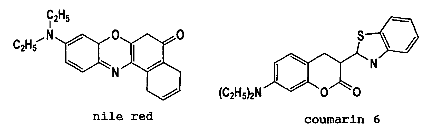
- nile red and coumarin 6 are shown below:
- the wavelength of light emitted by nile red is 580 nm (emission of red light) and that of coumarin 6 is 490 nm (emission of green light).
- emission center-forming compounds may be used either singly or in combination.
- a resin having film-forming properties e.g., a thermoplastic resin, a thermosetting resin
- a resin having film-forming properties e.g., a thermoplastic resin, a thermosetting resin
- thermoplastic resin examples include a olefinic resin such as a polyethylene, a polypropylene, an ethylene-propylene copolymer and a polybutene; a styrenic resin such as a polystyrene, a rubber-modified (or rubber-containing, rubber-reinforced) polystyrene (HIPS), an acrylonitrile-styrene copolymer and an acrylonitrile-butadiene-styrene copolymer; an acrylic resin [for example, a homo- or copolymer of a (meth)acrylic monomer (e.g., a C 1-6 alkyl (meth)acrylate such as methyl (meth)acrylate, ethyl (meth)acrylate and butyl (meth)acrylate, a hydroxyC 2-4 alkyl (meth)acrylate such as hydroxyethyl (meth)acrylate and hydroxypropyl (meth)
- thermosetting resin examples include a phenolic resin, an amino resin (e.g., a urea resin and a melamine resin), a thermosetting acrylic resin, an unsaturated polyester resin, an alkyd resin, a diallyl phthalate resin, an epoxy resin, and a silicone resin.
- the binder may be used singly or in combination.
- the content of the emission center-forming compound in the source is not particularly limited to a specific content, and is about 0.1 to 100% by weight, preferably about 1 to 90% by weight, and more preferably about 5 to 80% by weight.
- the content of the emission center-forming compound is not particularly limited to a specific content, and for example is about 0.1 to 60 parts by weight, preferably about 1 to 30 parts by weight, and more preferably about 3 to 20 parts by weight relative to 100 parts by weight of the binder.
- the source is usually used in the form of a film.
- the source may be a film or coat of the above emission center-forming compound singly formed on the substrate or the target, or that of the above emission center-forming compound and the binder.
- the substrate need only be sufficiently transparent to transmit laser beams, examples of which are a glass plate such as a soda glass, a no-alkali glass, and a quartz glass; and a polymer sheet or film of a polyester, a polystyrene, an acrylic resin, a vinyl-series resin (e.g., a polyvinyl acetal), a polysulfone, and of a polyethersulfone.
- a process of forming a source film there is no particular restriction as to a process of forming a source film, and a conventional process [e.g., dry processes such as vapor deposition (vacuum deposition), wet coating processes that use a solvent, such as spin coating, dip coating and die coating] may be employed.
- a conventional process e.g., dry processes such as vapor deposition (vacuum deposition), wet coating processes that use a solvent, such as spin coating, dip coating and die coating
- the film may be formed in accordance with a conventional film-forming process (e.g., casting method and extrusion method).
- the source may be incorporated a solvent (e.g., water; alcohols such as methanol and ethanol; esters such as ethyl acetate and isobutyl acetate; ketones such as acetone and methyl ethyl ketone; aromatic hydrocarbons such as toluene; alicyclic hydrocarbons such as cyclohexane; halogenated hydrocarbons such as chloroform and chlorobenzene; ethers; cellosolves; carbitols).
- the thickness of the film (coat) may be about 0.01 to 50 ⁇ m, preferably about 0.1 to 30 ⁇ m, and more preferably about 0.5 to 20 ⁇ m.
- the source may not be defined in a pattern, or the source itself may be defined in a given pattern.
- a film (layer, deposit) defined in a pattern, if necessary, on a substrate (base material) or a target may be used as a source.
- a film or sheet comprising an emission center-forming compound may be patterned by punching or other means to give a source.
- the substrate need only be sufficiently transparent to transmit laser beams, examples of which are a glass plate such as a soda glass, a no-alkali glass, and a quartz glass; and a polymer sheet or film of a polyester, a polystyrene, an acrylic resin, a vinyl-series resin (e.g., a polyvinyl acetal), a polysulfone, and of a polyethersulfone.
- a glass plate such as a soda glass, a no-alkali glass, and a quartz glass
- a polymer sheet or film of a polyester, a polystyrene, an acrylic resin, a vinyl-series resin (e.g., a polyvinyl acetal), a polysulfone, and of a polyethersulfone examples of which are a glass plate such as a soda glass, a no-alkali glass, and a quartz glass; and a polymer sheet or film of a polyester, a polyst
- the pattern is selected according to the intended application, and for example may be any of a one dimensional pattern [a dotted pattern, a lined pattern (e.g., parallel, random, grid)] and a two-dimensional pattern [a plane pattern (e.g., circular, oval, polygonal such as triangle and rectangle, star-shaped)].
- the predetermined pattern is provided on the substrate or the target by, for example, printing such as screen printing, ink jet system, melt or thermal transfer, or vapor deposition (sublimation printing) involving masking.
- the target has at least one function selected from the electron-transporting function and the hole-transporting function
- the target may be (I) a resin having at least one function selected from the electron-transporting function and the hole-transporting function, or (II) a resin composition comprising a resin which inherently has neither the electron-transporting function nor the hole-transporting function but given with at least one function selected from these.
- resins for the use of (I) and (II) resins (binder) having film- or coat-forming properties are preferred.
- the target is transmittable of the laser beam.
- a polyphenylenevinylene for example, a homo- or copolymer of a C- 6- 12 arylenevinylene, which may have a substituent (e.g., a C 1-10 alkoxy group), such as a polyphenylenevinylene, a poly(2,5-dimethoxyphenylenevinylene) and a polynaphthalenevinylene]; a polyphenylene (in particular, a polyparaphenylene) [for example, a homo- or copolymer of a phenylene, which may have a substituent (e.g., a C 1-10 alkoxy group), such as a polyparaphenylene and a poly-2,5-dimethoxyparaphenylene]; a polythiophene [a homo- or copolymer of a polyC 1-20 alkylthiophene such as
- the resin can be used either singly or in combination.
- the preferred target includes a copolymer comprising a poly-N-vinylcarbazole or N-vinylcarbazole as a main component (not less than 50% by weight, and preferably about 60 to 98% by weight), and a polymer having an aromatic amine derivative in a side chain or main chain thereof.
- PVK is amorphous and excellent in heat resistance (glass transition temperature Tg: 224°C).
- the degree of polymerization of PVK is not particularly restricted, and is, for example, about 200 to 5,000 (e.g., 300 to 3,000), and preferably about 500 to 2,000 (e.g., 500 to 1,500).
- the electron- or hole-transporting function may be given to the resin (I).
- Examples of the compound having an electron-transporting function are an oxadiazole derivative [for example, an oxadiazole derivative having a C 6-20 aryl group which may have a substituent, such as 2-(4-biphenyl)-5-(4-tert-butylphenyl)-1,3,4-oxadiazole (PBD), 2,5-bis(1-naphtyl)-1,3,4-oxadiazole (BND), 1,3-bis[5-(4-tert-butylphenyl]-1,3,4-oxadiazole)]benzene (BPOB), 1,3,5-tris[5-(4-tert-butylphenyl)-1,3,4-oxadiazole]benzene (TPOB) and 1,3,5-tris[5-(1-naphtyl)-1,3,4-oxadiazole]benzene (TNOB)]; a diphenoquinone [for example, a
- an aromatic tertiary amine such as N,N'-diphenyl-N,N'-bis(3-methylphenyl)-1,1'-biphenyl-4,4'-diamine (TPD), N.N'-diphenyl-N.N'-bis(1-naphthyl)-1,1'-biphenyl-4,4'-diamine (NPD), 1.1-bis[(di-4-tolylamino)phenyl]cyclohexane, N.N.N'N'-tetra(3-methylphenyl)-1,3-diaminobenzene (PDA), 4,4' , 4", tris (3 -methylphenylphenylamino) triphenylamine (m-MTDATA), 4.4'.4"-tris(1-naphthylphenylamino)triphenylamine(1-
- the above compound can be used either singly or in combination.
- a compound emitting a light by being excited by an electron and/or a hole may be used as an emission center-forming compound.
- the proportion of the above-mentioned component contained in the resin (I) can be selected within the range not adversely affecting the functions qualifying the resin as an organic EL device material, and is, for example, about 10 to 300 parts by weight, and preferably about 20 to 200 parts by weight relative to 100 parts by weight of the resin (I).
- the organic EL device which will later be described can be made so as to have a single-layered structure, and the organic EL device so fabricated not only has improved luminous efficiency but also is economically advantageous.
- a resin to be used in the resin composition (II) there is no specific restriction as to a resin to be used in the resin composition (II), and such a variety of above-mentioned binders having the film-forming properties (e.g., thermoplastic resins, thermosetting resins) are available. At least one function selected from the electron-transporting function and the hole-transporting function may be given to these resins. Exemplified as the compound(s) to be used to provide the electron- or hole-transporting function are compounds similar to those listed above.
- the amount of the compound having an electron-transporting or hole-transporting function to be added is about 10 to 300 parts by weight (e.g., about 10 to 200 parts by weight) and preferably about 20 to 100 parts by weight (e.g., about 20 to 80 parts by weight) relative to 100 parts by weight of the binder resin.
- the resin (I) and the resin composition (II) may be used in combination, and such combined material may further be given at least one function selected from the electron-transporting function and the hole-transporting function.
- a form (shape or configuration) of the target is not particularly limited to a specific form, and usually, is used in the form of a film. Moreover, the target is formed in the same manner as in the source, and usually is formed on the above-mentioned substrate.
- the process for producing materials for organic EL devices of the present invention comprises implanting an emission center-forming compound in a source into the target by irradiating (or exposing) a laser beam, and wherein (1) the laser beam and at least the target are relatively moved with irradiating the beam to form the emission center with a predetermined pattern, or (2) the emission center at an area, corresponding to an interference pattern of an interference light, of the target is formed by irradiating the interference light of the laser beam.
- the laser beam may be irradiated from the source (A) side or the target (B) side.
- a film is usually employed to produce a film for an organic EL device.
- the target may be brought into contact with the source.
- the laser beam to be used in the present invention are, though it differs with the species of the emission center-forming compound to be used, those having an oscillation wavelength within the range of 190 to 1,100 nm.
- the frequency is about 0.5 to 50 Hz and preferably about 0.5 to 30 Hz.
- the pulse width varies with the wavelength of the laser beam, it is about 10 ps to 10 ⁇ s (e.g., about 10 ps to 1 ⁇ s), preferably about 50 ps to 100 ns (e.g., about 100 ps to 50 ns). The shorter the pulse width (duration) is, the less the decomposition of the emission center-forming compound occurs, and therefore, the emission center-forming compound is hardly damaged.
- gas laser [ArF excimer laser (193 nm), KrF excimer laser (248 nm), XeCl excimer laser (308 nm), XeF excimer laser (351 nm), nitrogen laser (337 nm)]
- dye laser [nitrogen laser, excimer laser, or YAG laser excitation, 300 to 1,000 nm]
- solid-state laser [(Nd:YAG excitation, semiconductor laser excitation, etc.), ruby laser (694 nm), semiconductor laser (650 to 980 nm), tunable diode laser (630 to 1,550 nm), titanium-sapphire laser (Nd:YAG excitation, 345 to 500 nm, 690 to 1,000 nm), and Nd:YAG laser (FHG: 266 nm, THG: 354 nm, SHG: 532 nm, fundamental wave: 1,064 nm)].
- irradiation of a laser beam with an intensity of or below the ablation threshold of the source makes it possible to effectively implant the emission center-forming compound into the target.
- the amount of the emission center-forming compound to be implanted can be controlled by regulating, e.g., the intensity and wavelength of the laser beam, and the number of times the laser beam is shot.
- the ablation threshold of the source (A) varies with the species of the emission center-forming compound constituting the source. Moreover, the ablation threshold also depends on the wavelength and pulse width of the laser beam. Therefore, in the present invention, the ablation threshold is defined as follows.
- ablation threshold value used in the present invention is defined as a term referring to, assuming that a source is irradiated with one shot of a laser beam and observed by a contact-type (mode) surface morphology measuring apparatus (e.g., DEKTAK3030ST, manufactured by SLOAN), the lowest laser intensity (mJ/cm 2 ) measured on the surface irradiated with the laser beam at which the surface might suffer changes in surface conditions by a depth of 50 nm or more.
- the source and the laser beam are the same as those employed in the present invention.
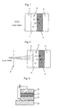
- Figure 1 shows a schematic view showing a production process in the method (1) of the present invention.
- Figure 2 shows a schematic view showing a production process in the method (2) of the present invention.
- a source 1, a target 2, an emission center-forming compound 3, a substrate resided in the target side 4, a substrate resided in the source side 5, and a hole 6 are illustrated in Figures.
- the source 1 formed on the substrate 5 is brought into contact with or closely contact with the target 2 formed on the substrate 4, and irradiated with a laser beam with an intensity of or below the ablation threshold of the source from the source 1 side with relatively moving the beam relative to the target.
- the emission center-forming compound, which absorbed the laser beam obtains high translational energy and is injected or implanted into the target 2 without being decomposed, and a material for an organic EL device (particularly, a film) is obtained.
- the source 1 formed on the substrate 5 is brought into contact with or closely contact with the target 2 formed on the substrate 4, and irradiated with a laser beam with an intensity of or below the ablation threshold of the source from the source 1 side with causing an interference by introducing the beam into a hole 6.
- the emission center-forming compound, which absorbed the laser beam obtains high translational energy and is injected or implanted into an area, corresponding to an interference pattern of the interference light, of the target 2 without being decomposed, and a material for an organic EL device (particularly, a film) is obtained.
- the laser beam is shot about 1 to 200 times, preferably about 1 to 150 times, and more preferably about 1 to 100 times (e.g., about 5 to 50 times).
- the laser beam may be shot from the target side.
- the source may be formed on the target directly as a surface layer. The source formed on the target can be removed from the target easily after implanting the emission-center compound. Moreover, the source may be formed by a surface layer removable or separable from the target.
- the substrate to be used need only have sufficient transparency to transmit a laser beam, examples of which are the above-mentioned substrates (e.g., a glass plate such as a quartz glass, a polymer sheet or film).
- a substrate used on forming of a source or a target film may be employed without modification, or a substrate produced freshly may be employed.
- the shape that the cross-section of the laser beam takes there is no particular restriction as to the shape that the cross-section of the laser beam takes, and it may be circular, oval, or polygonal (e.g., triangle, rectangle).
- the average beam area of the laser beam is not particularly limited to a specific area, and can be selected from a wide range for any purpose.
- the area is about 0.01 to 5,000 ⁇ m 2 , preferably about 0.1 to 4,000 ⁇ m 2 , and more preferably about 1 to 3,000 ⁇ m 2 .
- a pattern may be defined or formed by narrowing an area of a laser beam down a desired size and scanning a predetermined pattern, or an emission center-forming compound may be implanted into a target in a predetermined area by enlarging the area of the laser beam to use a source having a predetermined pattern or relatively scanning a laser beam through a photomask.
- a plurality of sources having emission center-forming compounds different from one another may be employed.
- the use of a compound capable of emitting a light in visible light region (a compound capable of emitting a light such as yellow, red, green or blue) realizes a desired emission color.
- the use of a plurality of sources realizes that an emission light such as red, green and blue can be arranged or arrayed as corresponding to an interference fringe or pattern (e.g., vertical stripe, delta arrangement and tetragonal arrangement). Therefore, the present invention makes it possible to obtain materials for organic EL devices capable of emitting various colors and having various patterns.
- the method (1) has a characteristic that the laser beam and at least the target are relatively moved for implanting an emission center-forming compound of a source into the target with a predetermined pattern.
- the source and the target are contacted with each other and positioned, and the source may be moved with the target, or the source may be movable relative to the target relatively.
- an irradiation of a laser beam may, for example, be conducted either by (1-1) moving a light path of the laser beam relative to the source and the target, or by (1-2) moving the source and the target relative to a light path of the laser beam.
- the light path of the laser beam is movable not only by moving a laser light source relatively but also (1-3) by using means for controlling the light path.
- the means for controlling the light path includes a process of utilizing physical means or physico-optical means [for example, an optical device (or optical member) such as an optical fiber, a reflection mirror (e.g., a total reflection mirror, a half reflection mirror), a lens (e.g., condenser) and a deflecting prism, or means in combination with them], a process of utilizing electro-optical means [(e.g., applying a voltage to an electro-optical crystal (a birefringent crystal)] to move a light path of a light beam of a waveguide, and a process of utilizing supersonic waves.
- an optical device or optical member
- a reflection mirror e.g., a total reflection mirror, a half reflection mirror
- a lens e.g., condenser
- deflecting prism e.g., condenser
- electro-optical means e.g., applying a voltage to an electro-optical crystal (a bire
- the waveguide in a process of utilizing supersonic waves, can be moved by using a crystalline material (such as water, a chalcogenide-series vitreous material, PbMoO4, TeO 2 , Ge, LiNbO 3 and GaP) as a medium, and applying a voltage to the medium through a piezoelectric thin film transducer (e.g., a piezoelectric device such as LiNbO 3 and ZnO) to generate supersonic waves to the medium.
- a crystalline material such as water, a chalcogenide-series vitreous material, PbMoO4, TeO 2 , Ge, LiNbO 3 and GaP
- a piezoelectric thin film transducer e.g., a piezoelectric device such as LiNbO 3 and ZnO
- the laser beam is capable of moving relatively and two-dimensionally relative to at least a target. Therefore, an emission center-forming compound of a source can be implanted into a target with a predetermined pattern efficiently, and the emission center can be formed in the form of a two-dimensional pattern.
- a target and a laser beam are relatively shifted by relatively moving the laser beam relative to at least the target according to the above-mentioned manner by synchronizing with a pulse cycle, and an emission center-forming compound can be implanted into a target efficiently.
- the target may be moved relative to the laser beam, and usually synchronizing with pulse cycle controls the laser beam or a light path of the laser beam.
- a laser beam may be relatively moved relative to at least a target, and a source may be moved relative to the laser beam.
- a source may be moved relative to the laser beam.
- a plurality of emission centers different from each other in emission color can be also formed efficiently.
- a plurality of areas comprising each of emission center-forming compounds e.g., an area comprising a yellow emission center-forming compound, an area comprising a red emission center-forming compound, and an area comprising a blue emission center-forming compound
- the use of such a source ensures that a plurality of emission centers different from each other in emission color can be formed with use of a single source by relatively moving the source relative to the laser beam and/or the target toward X-axial and/or Y-axial direction(s).
- Figure 7 shows a schematic view explaining another production process according to the method (1).
- a production process of a red emission center comprises moving a light path of a laser beam (light source or waveguide) relative to a target toward a longitudinal direction and/or a lateral direction, irradiating (or exposing) the laser beam to an area comprising a green emission center-forming compound of a source to form a green emission center into the target, moving the source relative to the laser beam, then irradiating the laser beam to an area comprising a red emission center-forming compound to form a red emission center into the target.
- a blue emission center is produced in the same manner as described above, and a material for an organic EL device capable of emitting a full-colored light can be produced.
- a pulse laser is irradiated (or emitted) to the target through the source with scanning toward a longitudinal direction and/or a lateral direction, and the source 1 and the target 2 is capable of contacting with each other at an irradiation site of the laser beam.
- the source 1 is movable to X-axial and/or Y-axial direction(s) by means of a feed apparatus.
- the use of a single source realizes that a plurality of emission centers different from each other in emission color are produced.
- An emission center-forming compound is used without wasting, the emission center-forming compound is implanted efficiently, and the process is advantageous in terms of cost.
- the source may be formed with an undefined length film or the like. The use of such a film realizes a continuous or successive production of an emission center-forming compound.
- the method (2) has a characteristic that the utilization of high coherence (coherency) of a laser beam realizes a production of an emission center into an area corresponding to an interference pattern of an interference light in the target by the interference light of the laser beam.
- "interference” also includes diffraction (considered as an interference of small wave (secondary wave) by the Principle of Huygens) ("Basis and Experiment of Laser", Koreiwa Matsudaira, issued by Kyoritsu Shuppan, Co., Ltd., the 11th edition, page 54).
- an interference of a laser beam may be obtained from optical path difference caused by splitting a laser beam from the single light source into a plurality of light paths.
- a process for interfering with a laser beam is not limited to one using a hole as shown in Figure 2, and for example, may be conducted either by (2-1) introducing a laser beam into a hole or a slit to cause an interference, or by (2-2) reflecting a laser beam through a plurality of reflection paths capable of reflecting to cause an interference.
- a slit width (in case of the hole, the average hole diameter) is not particularly limited, and is about 0.01 to 100 mm, preferably about 0.1 to 10 mm, and more preferably about 0.5 to 5 mm (e.g., about 0.5 to 3 mm).
- a shape of the hole there is no particular restriction as to a shape of the hole, and may be mentioned circular, oval, or polygonal (e.g., triangle, rectangle).
- the average diameter means an average diameter of circumscribed circle of the hole.
- the hole and the slit may be a single hole or slit, or each of them may be used plurally or in combination (e.g., double slit). Moreover, the hole and the slit may be used in combination.
- a laser beam guided by the hole or the slit is interfered by the optical path difference (in case of using a single hole or slit, diffracted), and interference fringe (or diffraction fringe) occurs.
- a mirror e.g., a semitransparent mirror, a reflecting mirror
- a semitransparent mirror ensures that an optical path difference between a transmitted light and a reflected light generates simply.
- the process comprises being incident a laser beam on a semitransparent mirror, which is disposed with gradient of a predetermined angle from an incident direction of the laser beam, transmitting part of the laser beam and reflecting the residual laser beam in an orthogonal direction to the incident direction of the laser beam.
- the transmitted light is incident on a first reflection mirror apart from the semitransparent mirror at a predetermined distance.
- the reflected light is incident on a second reflection mirror apart from the semitransparent mirror at a distance different from the above distance.
- a laser beam which is obtained by reflecting with use of the first and the second reflection mirror, going through a different reflection path and being incident on the semitransparent mirror again, is incident on the target, and as a result, an interference occurs by an optical path difference.
- a desired interference pattern can be obtained.
- each of the semitransparent mirror(s) and the reflection mirror(s) may be used singly or in combination.
- the laser beam may be made parallel pencil through a lens (such as a telemeter lens) and may be incident on the semitransparent mirror.
- a distance between interference fringes, or a shape (or form) of interference fringe can be adjusted by selecting parameters such as a hole diameter or a slit width and a mirror position suitably, and by varying an optical path distance.
- a desired interference pattern (interference fringe) can be obtained without through a mask and the like.
- the hole diameter or the slit width is turned down to a wavelength of the laser beam, interference fringe having a fine distance can be obtained, and fine patterning of an emission center-forming compound can be conducted easily.
- the interference fringe is usually a concentric pattern (symmetric figure) in which a center energy is most highest, the amount to be implanted of the emission center-forming compound can be adjusted.
- the production process of the present invention realizes that an emission center-forming compound is implanted into a target not in a dispersed or diffused form but in a step form (that is, an oblong form, in which the depth of the compound implanted into the target is uniform).
- the depth is varied depending on a kind or species of the emission center-forming compound or the target, or intensity of a laser beam, and for example, is about 10 to 300 nm, preferably about 15 to 200 nm, and more preferably about 20 to 100 nm.
- irradiation of the laser beam with an intensity of or below the ablation threshold value ensures that an emission center-forming compound is implanted efficiently without deterioration in surface smoothness of a material for an organic EL device.
- the organic electroluminescent device of the present invention comprises a material for an organic EL device obtained by the process described above (particularly, a light-emitting layer constituted of a target film into which an emission center-forming compound has been implanted) and a pair of electrodes.
- a transparent electrode formed by vacuum deposition or other methods e.g., indium-tin-oxide (ITO) electrode
- ITO indium-tin-oxide
- a highly conductive metal having a small work function e.g., magnesium, lithium, aluminum, or silver
- the magnesium may be coevaporated with a small amount of silver (e.g., 1 to 10% by weight) for improving the adhesion with an organic EL device-use film.
- the organic EL device of the present invention can be made so as to have a single-layered structure.
- a layer having the desired function may be laminated on the light-emitting layer by a conventional vapor deposition technique or a solution coating technique. These layers may be of low-molecular weight compounds or macromolecular compounds, and either will do.
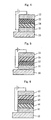
- the organic EL device can take, for example, a single-layer structure or a multilayer-structure as shown in Figures 3 to 6.
- the organic EL device may be one composed of a substrate 10, an anode 11 formed thereon, a light-emitting layer 12, and a cathode 13 laminated on the anode in this order, or, as shown in Figure 4, it may be one composed of a substrate 20, an anode 21 formed thereon, a hole-transporting layer 24, a light-emitting layer 22, and a cathode 23 laminated on the anode in this order.
- the organic EL device may be one composed of a substrate 30, an anode 31 formed thereon, a light-emitting layer 32, an electron-transporting layer 35, and a cathode 33 laminated on the anode in this order, or, as shown in Figure 6, it may be one composed of a substrate 40, an anode 41 formed thereon, a hole-transporting layer 44, a light-emitting layer 42, an electron-transporting layer 45, and a cathode 43 laminated on the anode in this order.
- each of the layers constituting the organic EL device is not particularly limited, and is about 10 nm to 1 ⁇ m(e.g., about 10 to 500 nm), preferably about 30 to 300 nm, more preferably about 30 to 200 nm, particularly about 5 to 20 nm.
- the thickness of each film can be selected within the ranges mentioned above.
- the substrate Exemplified as the substrate are those mentioned above, such as substrates having sufficient transparency to transmit laser beams (e.g., a glass plate, such as a soda glass, a no-alkali glass, and a quartz glass, a polymer sheet or film of a polyester, a polysulfone, and a polyethersulfone).
- a glass plate such as a soda glass, a no-alkali glass, and a quartz glass
- a polymer sheet or film of a polyester e.g., a soda glass, a no-alkali glass, and a quartz glass
- a polymer sheet or film of a polyester e.g., a polysulfone, and a polyethersulfone
- the substrate e.g., a substrate used on the molecular implantation may be employed without modification, or a substrate produced freshly may be employed.
- the present invention fine and multicolor patterning of an organic EL device made with macromolecular compounds which had long been difficult to realize was made possible. Further, since the material for the organic EL device (particularly, film for organic EL device) of the present invention is excellent in surface smoothness, it makes closely contact with the electrodes, and the organic EL device of the present invention is free from the irregularity in voltage caused upon application of voltage because of the emission center-forming compound implanted therein step-like.
- the present invention ensure that high positioning is conducted by relatively moving a laser beam relative to at least a target, fine patterning is conducted simply, and the use of an optical fiber realizes high-precision fine patterning. Moreover, an efficient implantation of emission center-forming compound is realized by relatively moving a laser beam and at least a target with moving a source relative to the laser beam.
- the utilization of high coherence (coherency) of a laser beam realizes a production of an emission center into an area corresponding to an interference pattern by an interference light of the laser beam. Since the interference pattern can be adjusted to a desired shape (form) and distance by selecting a parameter such as a hole diameter and a slit width suitably, fine patterning can be conducted simply.
- a polybutylmethacrylate (manufactured by Aldrich Chemical Company, Inc., molecular weight: 3.4 ⁇ 10 5 ) containing 5% by weight of coumarin 6 (manufactured by Nippon Kankoh Shikiso, K.K.) was dissolved in chlorobenzene, and a layer having 1 ⁇ m thick was produced on a quartz substrate by a spin coating method.
- a poly-N-vinylcarbazol having a hole-transporting function PVK: manufactured by Kanto Kagaku, K.K.
- PVK hole-transporting function
- PPD 2-(4-biphenyl)-5-(4-tert-butylphenyl)-1,3,4-oxadiazole having an electron-transporting function
- a coat layer of indium-tin-oxide (ITO) was formed on a glass substrate.
- ITO indium-tin-oxide
- An emission center-forming compound was implanted into a pattern having an area of 20 mm 2 by bringing thus obtained source film into contact with thus obtained target film, fixing them on a table movable for X-axial and Y-axial directions with a target film surface turning up, using a laser processing apparatus capable of oscillating XeF excimer laser (wavelength: 351 nm) having 10 ns of a pulse width at 20 mm 2 of a beam area, and moving the table relative to the laser beam toward X-Y-axial direction.
- a laser processing apparatus capable of oscillating XeF excimer laser (wavelength: 351 nm) having 10 ns of a pulse width at 20 mm 2 of a beam area, and moving the table relative to the laser beam toward X-Y-axial direction.
- a 200 nm thick Al/Li electrode (manufactured by Kohjundo Kagaku, K.K.; Li content: 0.78% by weight) was formed on the molecular-implanted target film (test piece 1) by vacuum deposition to provide an organic EL device 1.
- a target film was produced in the same manner as in Example 1.
- test piece constituted of two films obtained above being in contact with each other, was fabricated, and, from the direction of the target substrate, the test piece was irradiated with third harmonic of YAG laser (wavelength: 355 nm, pulse width: 3 ns, irradiation energy per unit area: 20 mJ/cm 2 , beam diameter: 1.8 mm) 10 times through a pinhole having a diameter of 1 mm.
- third harmonic of YAG laser wavelength: 355 nm, pulse width: 3 ns, irradiation energy per unit area: 20 mJ/cm 2 , beam diameter: 1.8 mm
- a 200 nm thick Al/Li electrode layer (manufactured by Kohjundo Kagaku, K.K.; Li content: 0.78% by weight) was formed on the molecular-implanted target film by vacuum deposition to provide an organic EL device.
- the ITO electrode of the above organic EL device as the anode
- the Al/Li electrode layer as the cathode
- a direct electric field was applied between the electrodes in the atmospheric air to cause the organic EL device to emit light.
- emission of light was observed.
- An emission form (shape) reflected that of light interference generated on the occasion when YAG laser beam passed through the pinhole, and emission ring pattern being green concentrically was observed.
- emission of blue due to PVK was observed
- emission of green light due to coumarin 6 was observed.
Landscapes
- Physics & Mathematics (AREA)
- Optics & Photonics (AREA)
- Engineering & Computer Science (AREA)
- Manufacturing & Machinery (AREA)
- Electroluminescent Light Sources (AREA)
Abstract
Description
Claims (17)
- A process for producing a material, for an organic electroluminescent device, having an emission center, which comprises implanting an emission center-forming compound constituting a source into a target having at least one function selected from the group consisting of an electron-transporting function and a hole-transporting function by irradiating a laser beam, and wherein(1) the laser beam and at least the target are relatively moved with irradiating the beam to form the emission center with a predetermined pattern, or(2) the emission center at an area, corresponding to an interference pattern of an interference light, of the target is formed by irradiating the interference light of the laser beam.
- A process according to claim 1, wherein, in the method (1), the source and the target being in contact with each other are moved relative to the laser beam for forming the emission center with a predetermined pattern.
- A process according to claim 1, wherein, in the method (1), the irradiation is conducted through a waveguide.
- A process according to claim 1, wherein, in the method (1), the irradiation is conducted with the use of an optical fiber.
- A process according to claim 1, wherein, in the method (1), the laser beam and the target are relatively moved with irradiating the beam and with moving the source relative to the beam for forming the emission center.
- A process according to claim 1, wherein, in the method (2), a laser beam from a single light source is split into a plurality of light paths to cause the interference by an optical path difference.
- A process according to claim 6, wherein the interference is caused by introducing the laser beam into a hole or a slit.
- A process according to claim 6, wherein the interference is caused by reflecting the laser beam through a plurality of reflection paths.
- A process according to claim 1, which comprises irradiating the laser beam with an intensity of or below the ablation threshold value of the source.
- A process according to claim 1, wherein the laser beam comprises a pulse laser beam.
- A process according to claim 10, wherein, in the method (1), the laser beam and the target are relatively moved with synchronizing the beam with a cycle of the pulse.
- A process according to claim 1, wherein the target comprises an organic polymer.
- A process according to claim 1, wherein the target comprises a compound having at least one function selected from the group consisting of the electron-transporting function and the hole-transporting function, and a film-formable organic polymer.
- A process according to claim 13, wherein the compound comprises at least one compound selected from the group consisting of an oxadiazole derivative having the electron-transporting function, and an aromatic tertiary amine having the hole-transporting function.
- A material for an organic electroluminescent device, which is obtainable by a process recited in claim 1.
- An organic electroluminescent device which comprises a pair of electrodes, and a material recited in claim 15 which is interposed between the electrodes.
- An organic electroluminescent device according to claim 16, wherein a single layer formed with a material in claim 12 is interposed between the pair of electrodes.
Applications Claiming Priority (5)
| Application Number | Priority Date | Filing Date | Title |
|---|---|---|---|
| JP2000387823A JP2002190386A (en) | 2000-12-20 | 2000-12-20 | Material for organic electroluminescence element and method for producing the same |
| JP2000387823 | 2000-12-20 | ||
| JP2000068611 | 2001-03-12 | ||
| JP2001068611A JP2002270370A (en) | 2001-03-12 | 2001-03-12 | Material for organic electroluminescence element, and its manufacturing method |
| PCT/JP2001/010966 WO2002051212A1 (en) | 2000-12-20 | 2001-12-14 | Material for organic electroluminescence device and its manufacturing method |
Publications (2)
| Publication Number | Publication Date |
|---|---|
| EP1347670A1 true EP1347670A1 (en) | 2003-09-24 |
| EP1347670A4 EP1347670A4 (en) | 2009-01-14 |
Family
ID=26606211
Family Applications (1)
| Application Number | Title | Priority Date | Filing Date |
|---|---|---|---|
| EP01271789A Pending EP1347670A4 (en) | 2000-12-20 | 2001-12-14 | MATERIAL FOR ELECTROLUMINESCENT DEVICES AND ITS MANUFACTURING METHOD |
Country Status (4)
| Country | Link |
|---|---|
| US (1) | US6797920B2 (en) |
| EP (1) | EP1347670A4 (en) |
| KR (1) | KR20020077484A (en) |
| CN (1) | CN1401204A (en) |
Cited By (9)
| Publication number | Priority date | Publication date | Assignee | Title |
|---|---|---|---|---|
| US8334057B2 (en) | 2005-06-08 | 2012-12-18 | Semiconductor Energy Laboratory Co., Ltd. | Light-emitting element, light-emitting device, and electronic device |
| US8734915B2 (en) | 2008-02-29 | 2014-05-27 | Semiconductor Energy Laboratory Co., Ltd. | Film-formation method and manufacturing method of light-emitting device |
| US20160005608A1 (en) * | 2004-09-24 | 2016-01-07 | President & Fellows Of Harvard College | Femtosecond Laser-Induced Formation Of Submicrometer Spikes On A Semiconductor Substrate |
| US10229951B2 (en) | 2010-04-21 | 2019-03-12 | Sionyx, Llc | Photosensitive imaging devices and associated methods |
| US10244188B2 (en) | 2011-07-13 | 2019-03-26 | Sionyx, Llc | Biometric imaging devices and associated methods |
| US10269861B2 (en) | 2011-06-09 | 2019-04-23 | Sionyx, Llc | Process module for increasing the response of backside illuminated photosensitive imagers and associated methods |
| US10347682B2 (en) | 2013-06-29 | 2019-07-09 | Sionyx, Llc | Shallow trench textured regions and associated methods |
| US10374109B2 (en) | 2001-05-25 | 2019-08-06 | President And Fellows Of Harvard College | Silicon-based visible and near-infrared optoelectric devices |
| US10505054B2 (en) | 2010-06-18 | 2019-12-10 | Sionyx, Llc | High speed photosensitive devices and associated methods |
Families Citing this family (4)
| Publication number | Priority date | Publication date | Assignee | Title |
|---|---|---|---|---|
| US7338820B2 (en) * | 2002-12-19 | 2008-03-04 | 3M Innovative Properties Company | Laser patterning of encapsulated organic light emitting diodes |
| US20080233297A1 (en) * | 2007-03-23 | 2008-09-25 | Xerox Corporation | Methods of forming a photoreceptor device having a self-assembled patterned binder layer |
| US20160233425A1 (en) * | 2013-10-01 | 2016-08-11 | Sumitomo Chemical Company, Limited | Light emitting device |
| CN110504389B (en) * | 2019-08-14 | 2022-07-05 | 昆山国显光电有限公司 | Preparation method of light-emitting device, light-emitting device and display panel |
Family Cites Families (16)
| Publication number | Priority date | Publication date | Assignee | Title |
|---|---|---|---|---|
| JPS59123193A (en) | 1982-12-29 | 1984-07-16 | 日本精機株式会社 | Field light emitting display element |
| JPH06297457A (en) | 1993-04-17 | 1994-10-25 | Kanegafuchi Chem Ind Co Ltd | Manufacturing method of functional materials |
| JPH08106006A (en) | 1994-10-05 | 1996-04-23 | Dainippon Ink & Chem Inc | Dye molecule injection method, image forming method, and color filter manufacturing method |
| JP3509385B2 (en) | 1995-07-24 | 2004-03-22 | 株式会社リコー | Toner bottle |
| JPH0963770A (en) | 1995-08-24 | 1997-03-07 | Kemipuro Kasei Kk | Single layer white light emitting organic EL device |
| US6566156B1 (en) * | 1996-06-12 | 2003-05-20 | The Trustees Of Princeton University | Patterning of thin films for the fabrication of organic multi-color displays |
| US5714301A (en) * | 1996-10-24 | 1998-02-03 | Eastman Kodak Company | Spacing a donor and a receiver for color transfer |
| KR20010021742A (en) * | 1997-07-11 | 2001-03-15 | 게리 더블유. 존스 | Laser ablation method to fabricate color organic light emitting diode displays |
| JP4547723B2 (en) | 1998-03-09 | 2010-09-22 | セイコーエプソン株式会社 | Manufacturing method of organic EL display device |
| JPH11302393A (en) | 1998-04-21 | 1999-11-02 | Japan Atom Energy Res Inst | Laser-driven molecular injection into polymer solids using organic molecule-dispersed polymer pellets |
| KR100282393B1 (en) * | 1998-06-17 | 2001-02-15 | 구자홍 | method for fabricating Organic Electroluminescent display Device |
| JP3468450B2 (en) | 1998-07-17 | 2003-11-17 | 科学技術振興事業団 | Method for selective reforming inside solid material and solid material having selectively reformed inside |
| KR100625730B1 (en) * | 1998-09-01 | 2006-09-20 | 다이셀 가가꾸 고교 가부시끼가이샤 | Material for organic electroluminescent device and manufacturing method thereof |
| JP3532469B2 (en) | 1998-09-01 | 2004-05-31 | ダイセル化学工業株式会社 | Material for organic electroluminescence element and method for producing the same |
| JP3621283B2 (en) | 1999-03-05 | 2005-02-16 | 日本原子力研究所 | Method of injecting organic molecules into small regions in polymer solids |
| JP3545981B2 (en) | 1999-12-09 | 2004-07-21 | ダイセル化学工業株式会社 | Material for organic electroluminescence element and method for producing the same |
-
2001
- 2001-12-14 EP EP01271789A patent/EP1347670A4/en active Pending
- 2001-12-14 CN CN01805026A patent/CN1401204A/en active Pending
- 2001-12-14 KR KR1020027010799A patent/KR20020077484A/en not_active Withdrawn
- 2001-12-14 US US10/203,476 patent/US6797920B2/en not_active Expired - Fee Related
Cited By (13)
| Publication number | Priority date | Publication date | Assignee | Title |
|---|---|---|---|---|
| US10374109B2 (en) | 2001-05-25 | 2019-08-06 | President And Fellows Of Harvard College | Silicon-based visible and near-infrared optoelectric devices |
| US10361083B2 (en) | 2004-09-24 | 2019-07-23 | President And Fellows Of Harvard College | Femtosecond laser-induced formation of submicrometer spikes on a semiconductor substrate |
| US10741399B2 (en) | 2004-09-24 | 2020-08-11 | President And Fellows Of Harvard College | Femtosecond laser-induced formation of submicrometer spikes on a semiconductor substrate |
| US20160005608A1 (en) * | 2004-09-24 | 2016-01-07 | President & Fellows Of Harvard College | Femtosecond Laser-Induced Formation Of Submicrometer Spikes On A Semiconductor Substrate |
| US9263645B2 (en) | 2005-06-08 | 2016-02-16 | Semiconductor Energy Laboratory Co., Ltd. | Light-emitting element, light-emitting device, and electronic device |
| US8334057B2 (en) | 2005-06-08 | 2012-12-18 | Semiconductor Energy Laboratory Co., Ltd. | Light-emitting element, light-emitting device, and electronic device |
| US8734915B2 (en) | 2008-02-29 | 2014-05-27 | Semiconductor Energy Laboratory Co., Ltd. | Film-formation method and manufacturing method of light-emitting device |
| US10229951B2 (en) | 2010-04-21 | 2019-03-12 | Sionyx, Llc | Photosensitive imaging devices and associated methods |
| US10505054B2 (en) | 2010-06-18 | 2019-12-10 | Sionyx, Llc | High speed photosensitive devices and associated methods |
| US10269861B2 (en) | 2011-06-09 | 2019-04-23 | Sionyx, Llc | Process module for increasing the response of backside illuminated photosensitive imagers and associated methods |
| US10244188B2 (en) | 2011-07-13 | 2019-03-26 | Sionyx, Llc | Biometric imaging devices and associated methods |
| US10347682B2 (en) | 2013-06-29 | 2019-07-09 | Sionyx, Llc | Shallow trench textured regions and associated methods |
| US11069737B2 (en) | 2013-06-29 | 2021-07-20 | Sionyx, Llc | Shallow trench textured regions and associated methods |
Also Published As
| Publication number | Publication date |
|---|---|
| CN1401204A (en) | 2003-03-05 |
| EP1347670A4 (en) | 2009-01-14 |
| KR20020077484A (en) | 2002-10-11 |
| US20030075533A1 (en) | 2003-04-24 |
| US6797920B2 (en) | 2004-09-28 |
Similar Documents
| Publication | Publication Date | Title |
|---|---|---|
| JP4345278B2 (en) | PATTERNING METHOD, FILM FORMING METHOD, PATTERNING APPARATUS, ORGANIC ELECTROLUMINESCENCE ELEMENT MANUFACTURING METHOD, COLOR FILTER MANUFACTURING METHOD, ELECTRO-OPTICAL DEVICE MANUFACTURING METHOD, AND ELECTRONIC DEVICE MANUFACTURING METHOD | |
| US6797920B2 (en) | Material for organic electroluminescent device and its manufacturing method | |
| KR101202515B1 (en) | Methods of making displays | |
| US6690109B2 (en) | Organic electroluminescence element and manufacturing method thereof | |
| US20070080634A1 (en) | Thermal transfer of light-emitting dendrimers | |
| EP1043915B1 (en) | Material for organic electroluminescence device and method for producing the same | |
| KR100611156B1 (en) | Donor substrate for laser transfer and organic electroluminescent element manufactured using the substrate | |
| WO2002051212A1 (en) | Material for organic electroluminescence device and its manufacturing method | |
| KR100543000B1 (en) | Donor film for full color organic electroluminescent element, manufacturing method of donor film, and full color organic electroluminescent element using this donor film | |
| EP1107331A2 (en) | Material for organic electroluminescence device and process for producing the same | |
| JP3545981B2 (en) | Material for organic electroluminescence element and method for producing the same | |
| JP3532469B2 (en) | Material for organic electroluminescence element and method for producing the same | |
| JP2002270370A (en) | Material for organic electroluminescence element, and its manufacturing method | |
| JP2005158357A (en) | Diffusion method and electroluminescent material | |
| JP2002030283A (en) | Material for organic electroluminescence element and method for producing the same | |
| HK1036819A (en) | Material for organic electroluminescence device and process for producing the same | |
| JP2005108749A (en) | Source composition and method for producing material for organic electroluminescence device | |
| HK1030130B (en) | Material for organic electroluminescence device and method for producing the same | |
| KR20070031914A (en) | Deposition method of organic layer for OLD | |
| JP2002015864A (en) | Method of manufacturing organic electroluminescent element | |
| JP2007087642A (en) | Donor film for full color organic light emitting device, method for producing full color organic light emitting device, full color organic light emitting device and use thereof |
Legal Events
| Date | Code | Title | Description |
|---|---|---|---|
| PUAI | Public reference made under article 153(3) epc to a published international application that has entered the european phase |
Free format text: ORIGINAL CODE: 0009012 |
|
| 17P | Request for examination filed |
Effective date: 20020807 |
|
| AK | Designated contracting states |
Kind code of ref document: A1 Designated state(s): AT BE CH CY DE DK ES FI FR GB GR IE IT LI LU MC NL PT SE TR |
|
| RIN1 | Information on inventor provided before grant (corrected) |
Inventor name: KITAGUCHI, TORU Inventor name: KAMBARA, SHIGEKI |
|
| RBV | Designated contracting states (corrected) |
Designated state(s): AT BE GB NL |
|
| REG | Reference to a national code |
Ref country code: DE Ref legal event code: 8566 |
|
| RAP1 | Party data changed (applicant data changed or rights of an application transferred) |
Owner name: DAICEL CHEMICAL INDUSTRIES, LTD. |
|
| A4 | Supplementary search report drawn up and despatched |
Effective date: 20081215 |
|
| STAA | Information on the status of an ep patent application or granted ep patent |
Free format text: STATUS: THE APPLICATION IS DEEMED TO BE WITHDRAWN |