EP1347389A2 - Bus twisting scheme for distributed coupling and low power - Google Patents
Bus twisting scheme for distributed coupling and low power Download PDFInfo
- Publication number
- EP1347389A2 EP1347389A2 EP03006069A EP03006069A EP1347389A2 EP 1347389 A2 EP1347389 A2 EP 1347389A2 EP 03006069 A EP03006069 A EP 03006069A EP 03006069 A EP03006069 A EP 03006069A EP 1347389 A2 EP1347389 A2 EP 1347389A2
- Authority
- EP
- European Patent Office
- Prior art keywords
- lines
- line
- bus
- twisted
- twisting
- Prior art date
- Legal status (The legal status is an assumption and is not a legal conclusion. Google has not performed a legal analysis and makes no representation as to the accuracy of the status listed.)
- Granted
Links
Images




Classifications
-
- G—PHYSICS
- G06—COMPUTING OR CALCULATING; COUNTING
- G06F—ELECTRIC DIGITAL DATA PROCESSING
- G06F13/00—Interconnection of, or transfer of information or other signals between, memories, input/output devices or central processing units
- G06F13/38—Information transfer, e.g. on bus
- G06F13/40—Bus structure
- G06F13/4063—Device-to-bus coupling
- G06F13/4068—Electrical coupling
- G06F13/4086—Bus impedance matching, e.g. termination
-
- G—PHYSICS
- G06—COMPUTING OR CALCULATING; COUNTING
- G06F—ELECTRIC DIGITAL DATA PROCESSING
- G06F30/00—Computer-aided design [CAD]
- G06F30/30—Circuit design
- G06F30/39—Circuit design at the physical level
-
- G—PHYSICS
- G11—INFORMATION STORAGE
- G11C—STATIC STORES
- G11C7/00—Arrangements for writing information into, or reading information out from, a digital store
- G11C7/02—Arrangements for writing information into, or reading information out from, a digital store with means for avoiding parasitic signals
-
- G—PHYSICS
- G11—INFORMATION STORAGE
- G11C—STATIC STORES
- G11C7/00—Arrangements for writing information into, or reading information out from, a digital store
- G11C7/10—Input/output [I/O] data interface arrangements, e.g. I/O data control circuits, I/O data buffers
- G11C7/1048—Data bus control circuits, e.g. precharging, presetting, equalising
-
- G—PHYSICS
- G11—INFORMATION STORAGE
- G11C—STATIC STORES
- G11C7/00—Arrangements for writing information into, or reading information out from, a digital store
- G11C7/18—Bit line organisation; Bit line lay-out
-
- Y—GENERAL TAGGING OF NEW TECHNOLOGICAL DEVELOPMENTS; GENERAL TAGGING OF CROSS-SECTIONAL TECHNOLOGIES SPANNING OVER SEVERAL SECTIONS OF THE IPC; TECHNICAL SUBJECTS COVERED BY FORMER USPC CROSS-REFERENCE ART COLLECTIONS [XRACs] AND DIGESTS
- Y02—TECHNOLOGIES OR APPLICATIONS FOR MITIGATION OR ADAPTATION AGAINST CLIMATE CHANGE
- Y02D—CLIMATE CHANGE MITIGATION TECHNOLOGIES IN INFORMATION AND COMMUNICATION TECHNOLOGIES [ICT], I.E. INFORMATION AND COMMUNICATION TECHNOLOGIES AIMING AT THE REDUCTION OF THEIR OWN ENERGY USE
- Y02D10/00—Energy efficient computing, e.g. low power processors, power management or thermal management
Definitions
- One embodiment of the present invention relates to bus twisting method.
- one embodiment of the present invention relates to an algorithm used to twist bus lines or wiring resulting in distributed coupling, lower capacitance and low power.
- Memory structures have become integral parts of modern VLSI systems, including digital line processing systems. Although typically it is desirable to incorporate as many memory cells as possible into a given area, memory cell density is usually constrained by other design factors such as layout efficiency, performance, power requirements, and noise sensitivity.
- SRAM static random access memory
- DRAM dynamic RAM
- SRAM subsystems of many VLSI systems frequently are integrated relative to particular design implementations, with specific adaptations of the SRAM subsystem limiting, or even precluding, the scalability of the SRAM subsystem design.
- SRAM memory subsystem designs even those considered to be "scalable”, often fail to meet such design limitations once these memory subsystem designs are scaled-up for use in a VLSI system needing a greater memory cell population and/or density.
- a number of such memory structures including SRAM modules or subsystems, not to mention the VLSI systems themselves among other systems and devices, have a number of lines, bitlines for example, that physically run in parallel (alternatively referred to as a "bus"). Switching one of the bitlines up and down on the bus may cause the other lines in spaced relationship to the switching lines, lines above and below for example, to couple with the switching lines, thus increasing the capacitance and power requirements of at least the line, if not the entire bus.
- One embodiment of the present invention relates to a method for equalizing the capacitance between at least two lines.
- the method includes determining a twisting pattern for the lines using an algorithm. After determining the twisting pattern, the lines are twisted according to the pattern so that each of the lines runs along every other line for a same distance across the length of the bus.
- One embodiment of the present invention relates to a method for equalizing the capacitance between at least two lines. This method includes determining a twisting pattern for the lines, then twisting the lines according to said pattern so that each of the lines runs along every other line for a same distance across at least a portion of the length thereof.
- Yet another embodiment of the present invention relates to a device having at a plurality of lines, where at least two lines run in parallel for at least a portion of their length. These lines are twisted so each line runs along every other line for a same distance.
- One embodiment of the present invention provides a memory device having at least one logical memory subsystem and a plurality of lines connected to the logical memory subsystem, where the lines running parallel for at least a portion of their length.
- the lines are twisted according to an algorithm so that a capacitance of the lines is equalized.
- one embodiment of the present invention may be used with a memory architecture such as a SRAM module or subsystem similar to the SRAM module illustrated in commonly assigned U.S. Application No. 10/100,757 filed March 19, 2003, titled “Synchronously Controlled, Self-Timed Local SRAM Block", the complete subject matter of which is incorporated herein by reference in its entirety.
- one embodiment of the present invention may be used with the disclosed Local Sense Amp including a plurality of untwisted bitlines, bit and bit_n for example, that physically run in parallel.
- the present invention is discussed with respect to a multiple bitlines in a memory architecture, a SRAM module or other memory device for example, it is contemplated that the present invention may be used with any system or device having a plurality of lines running in parallel, including busses on chips or boards for example, wherein switching one line may cause one or more of the other lines to switch.
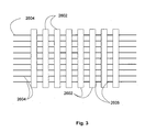
- FIG. 1 One example of an untwisted 9-bit bus line generally designated 2400 is illustrated in Fig. 1. Switching one of the bitlines 2402 up and down may cause the other lines, in spaced relationship to the switching lines, to couple with the switching lines, increasing the capacitance and power requirements of the bus 2400 and the bitlines 2402 on the bus.
- shielded lines or power rails to separate the bitlines from nearby pairs, reducing coupling capacitance on the bus.
- Using such shield lines take up space in the memory structure. Furthermore, such shield lines have their own power requirements.
- One embodiment of the present invention relates to minimizing the worst case power dissipation in a bus, having multiple parallel lines running along every other line in the bus for the same length. More particularly, one embodiment of the present invention relates to twisting a bus (similar to bus 2400 of Fig. 1) of multiple interconnect lines or bitline (similar to bitlines 2402) for the purpose of equalizing the capacitance between any two of the bit lines and reducing the maximum power dissipation. It should be appreciated that, if the bus switching (i.e., rising and falling transitions) are driven at different times, power dissipation may be reduced even further, as discussed below. Furthermore, if one of the bus lines is used as a reference, the power dissipation may be reduced even further through the use of limited swing techniques.
- One embodiment of the present invention provides for twisting a set of n bus lines such that each line is coupled to every other line equally and each line runs along every other line in the bus for the same amount of distance across the length of the bus.
- One embodiment of the present invention provides for using either n -1 or n identical twisting sections.
- line 1 is connected to line 0 (i.e., line i goes to 0 is line 1 goes to 0).
- Fig. 1 illustrates one embodiment of an untwisted bus 2400 of 9 lines 2402 as mentioned above.
- each line is capacitively coupled to its immediate neighbors (or neighbor) over the entire length of the bus, but is not coupled (to the first order) to more distant lines.
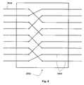
- twisting pattern in each section 2602 is the same. As a result, assembling a memory subsystem, or any other system having a bus or parallel lines, using the twisting sections 2602 is straight forward, as the pattern is simply repeated n - 1 (or n times) as provided below.
- twisting section 2062 containing twisted bus lines 2608 is illustrated in Fig. 4.
- Fig. 5 illustrates an embodiment of a twisted bus 2800 with n twisting sections 2802, 9 for example, in accordance with the present invention. All the bus lines 2804 are equally coupled similar to that described previously. In this embodiment, sections 2804 are all the same length except section 2808, where section 2808 is used to de-scramble the output. In one embodiment, section 2808 has a length of zero.
- Fig. 6 illustrates one embodiment of the present invention comprises a compact layout 2900, where the interconnection is implemented on at least two metal layers. Several vias or interconnects 2902 are used at the metal interconnection points to reduce the overall contact resistance.
- the bus may be broken up into smaller bundles. For example if a wide bus contains 256 lines, the bus may be broken down into 32 bundles of 8 lines each. Each bundle may be individually twisted.
- a shield line similar to the shield lines illustrated in Fig. 12 may be inserted between adjacent bundles. The shield lines are adapted to prevent unequalized coupling between bus lines in adjacent bundles.
- Yet another embodiment of the present invention comprises staggering the bitlines, or more particularly staggering the signals on the bitlines of a bus.
- a plurality of buffers 3000 (best viewed in Fig. 7) interface with at least one end of the bitlines, adapted to stagger the bitlines, or at least the signals or data on the bitlines. Staggering the lines reduces the maximum power consumption.
- coupling capacitance for twisted bus is 1 ⁇ 2 of that for untwisted bus.
- Data is transmitted across the lines in the bus at frequency f .
- each line of the bus rises from VSS to VDD (i.e., switching up), falls from VDD to VSS (i.e., switching down) or remains the same if the data is unchanged from one cycle to the next.
- the capacitance for the full length of the bus between any one line on the bus and its immediate neighbor is represented as C C .
- the capacitance between any particular line and ground is represented as C G .
- the maximum power dissipation in all cases occurs when all the bus lines are switching, but each line is switching in the opposite direction to its two neighbors.
- Fig. 7 illustrates buffer 3000 in accordance with one embodiment of the present invention.
- buffer 3000 comprises two inverters 3002 and 3004, where the output of inverter 3002 is coupled to the input of inverter 3004.
- each inverter has a PMOS transistor, 3002A and 3004A, and a NMOS transistor, 3002B and 3004B.
- the two inverters 3002 and 3004 are skewed so that NMOS in 3002 and PMOS in 3004 are larger than the symmetric ratio. This arrangement results in a rising transition that propagates faster than a falling transition, thereby causing an output buffer (not shown) to switch up earlier (i.e., faster) than it switches down.
- the data or signal transmitted on any of the lines is switched from VSS to VDD (alternatively referred to as "rail-to-rail").
- data may be transmitted on any of the lines in one direction from 0 to VDD, or on in the other direction, from VDD to 0 as provided above.
- using an amplifier 3100 as illustrated in Fig. 8 amplifies a limited swing voltage.
- amplifier 3100 may amplify the limited swing voltage to a full rail-to-rail voltage or some lesser voltage for example. It takes less power and is faster to switch the limited swing voltage than to switch a rail-to-rail voltage.
- the amplifier 3100 may have paired bitlines comprising a reference input signal and comparable input signals that are distinguishable or far enough apart from the reference input signal so the amplifier 3100 makes a correct determination.
- amplifier 3100 includes an input 3102 for the high or low signals 3102 (alternatively referred to as "H" and "L") and an input 3104 for the reference signal.
- the input H may be equal to VDD, for example, input L may be equal to VDD - 200mv, while the reference may be equal to (H + L)/2.
- a large number of amplifiers 3100 are generally required, each amplifier having a reference input and associated signal input for comparison.
- a large bus may have 8 amplifiers, each amplifier 3100 having a reference input 3104 and its own input signal 3102. (H/L inputs).
- one embodiment of the present invention comprises twisting one reference line with a plurality of input lines.
- a reference line 3200 is twisted with 7 signal lines 3202A, 3202B, 3202C, 3202D, 3202E, 3202F, 3202G, and 3202H according to the algorithm discussed above. It should be appreciated that, in this embodiment, the reference line 3200 runs along every other line 3202A-3202H for the same distance, similar to that described above.
- the voltage drop for any one input line depends on its distance from the reference line 3200. However, in this embodiment, with twisting the reference line 3200 runs along every other line 3202A-3202H for the same distance, so that the drop for each line 3202 is the same. For example if 7 input lines are twisted with one reference line 3200, and the voltage across two input lines is dropped (6 lines aren't dropped), the total voltage drop is the same so that all the lines are pulled down by the same amount as illustrated in Fig. 10. If however the voltage on 7 lines is dropped and 1 line isn't, the voltage drop is still the same (i.e., the swing about the reference line is the same), although total drop is greater as illustrated in Fig. 11.
Landscapes
- Engineering & Computer Science (AREA)
- Theoretical Computer Science (AREA)
- Computer Hardware Design (AREA)
- General Engineering & Computer Science (AREA)
- Physics & Mathematics (AREA)
- General Physics & Mathematics (AREA)
- Evolutionary Computation (AREA)
- Geometry (AREA)
- Design And Manufacture Of Integrated Circuits (AREA)
- Dram (AREA)
Abstract
Description
| [A] i is even and less than n-2 | line i goes to line i+2 |
| [B] i is even and equals n-2 | line i goes to line n-1 |
| [C] i is even and equals n-1 | line i goes to line n-2 |
| [D] i is odd and greater than 1 | line i goes to line i-2 |
| [E] i equals 1 | line i goes to |
| Maximum power | |
| Untwisted bus | |
| 1 / 2fV 2(4CC + CG ) | |
| | 1 / 2fV 2(2CC + CG ) |
| Untwisted staggered | 1 / 2fV 2 (2CC + CG ) |
| Twisted staggered | 1 / 2fV 2 (CC + CG ) |
Claims (20)
- A method for equalizing the capacitance between at least two lines, the method comprising:determining a twisting pattern for the lines; andtwisting the lines according to said pattern so that each of the lines runs along every other line for a same distance.
- The method of Claim 1, wherein said twisting pattern is determined according to an algorithm.
- The method of Claim 1, further including staggering switching transitions for the lines.
- The method of Claim 3, wherein staggering said switching transition includes switching up transitions.
- The method of Claim 3, wherein staggering said switching transitions includes switching down transitions.
- The method of Claim 1, including twisting at least a portion of the lines according to said twisting pattern, forming at least one twisting section.
- The method of Claim 6, further including forming a plurality of twisted sections.
- The method of Claim 7, including forming n twisted sections for n lines.
- The method of Claim 7, including forming n - 1 twisted sections for n lines.
- A method for reducing power consumption in a bus line, said method comprising:staggering switching up and switching down transition in time;and skewing at least one inverter.
- A method for equalizing the capacitance between at a plurality of lines forming a bus running in parallel for a portion of their length, the method comprising:determining a twisting pattern for the lines; andtwisting the lines according to said pattern so that each of the lines runs along every other line for a same distance across the length of the bus.
- A device having at a plurality of lines comprising at least two lines running in parallel for at least a portion of their length, wherein the lines are twisted so each line runs along every other line for a same distance.
- The device of Claim 12, wherein the lines are twisted according to an algorithm.
- A memory device comprising;at least one logical memory subsystem; andand a plurality of lines connected to said logical memory subsystem running in parallel for at least a portion of their length, wherein said lines are twisted to equalize a capacitance of said lines.
- The memory device of Claim 14, further including at least one twisting section containing said plurality of twisted lines.
- The memory device of Claim 14, further including a plurality of twisted sections, each said section containing said plurality of twisted lines.
- The memory device of Claim 16, wherein for n number of lines there are n twisted sections.
- The memory device of Claim 16, wherein for n number of lines there are n - 1 twisted sections.
- The memory device of Claim 14, including a staggering device adapted to stagger data on said lines in at least two different directions.
- The memory device of claim 19, including an amplifying device adapted to limit a swing voltage on said lines.
Applications Claiming Priority (4)
| Application Number | Priority Date | Filing Date | Title |
|---|---|---|---|
| US100872 | 1998-06-22 | ||
| US10/100,872 US6894231B2 (en) | 2002-03-19 | 2002-03-19 | Bus twisting scheme for distributed coupling and low power |
| US10/100,757 US6646954B2 (en) | 2001-02-02 | 2002-03-19 | Synchronous controlled, self-timed local SRAM block |
| US100757 | 2002-03-19 |
Publications (3)
| Publication Number | Publication Date |
|---|---|
| EP1347389A2 true EP1347389A2 (en) | 2003-09-24 |
| EP1347389A3 EP1347389A3 (en) | 2010-04-07 |
| EP1347389B1 EP1347389B1 (en) | 2013-05-15 |
Family
ID=27791207
Family Applications (1)
| Application Number | Title | Priority Date | Filing Date |
|---|---|---|---|
| EP03006069.3A Expired - Lifetime EP1347389B1 (en) | 2002-03-19 | 2003-03-19 | Bus twisting scheme for equalizing coupling and low power |
Country Status (1)
| Country | Link |
|---|---|
| EP (1) | EP1347389B1 (en) |
Cited By (1)
| Publication number | Priority date | Publication date | Assignee | Title |
|---|---|---|---|---|
| US7221577B2 (en) * | 2002-03-19 | 2007-05-22 | Broadcom Corporation | Bus twisting scheme for distributed coupling and low power |
Family Cites Families (3)
| Publication number | Priority date | Publication date | Assignee | Title |
|---|---|---|---|---|
| JPH10107208A (en) * | 1996-09-30 | 1998-04-24 | Toshiba Corp | Semiconductor integrated circuit device |
| KR100300047B1 (en) * | 1998-05-30 | 2001-09-22 | 김영환 | Semicondcutor device with data line arrangement for preventing of noise interference |
| US6188598B1 (en) * | 1999-09-28 | 2001-02-13 | Infineon Technologies North America Corp. | Reducing impact of coupling noise |
-
2003
- 2003-03-19 EP EP03006069.3A patent/EP1347389B1/en not_active Expired - Lifetime
Non-Patent Citations (1)
| Title |
|---|
| "Low-Power SRAM Design Using Half-Swing Puls-Mode Techniques", IEEE JOURNAL OF SOLID STATE CIRCUITS, vol. 33, no. 11, November 1988 (1988-11-01) |
Cited By (1)
| Publication number | Priority date | Publication date | Assignee | Title |
|---|---|---|---|---|
| US7221577B2 (en) * | 2002-03-19 | 2007-05-22 | Broadcom Corporation | Bus twisting scheme for distributed coupling and low power |
Also Published As
| Publication number | Publication date |
|---|---|
| EP1347389B1 (en) | 2013-05-15 |
| EP1347389A3 (en) | 2010-04-07 |
Similar Documents
| Publication | Publication Date | Title |
|---|---|---|
| US7215561B2 (en) | Semiconductor memory system having multiple system data buses | |
| US8143966B2 (en) | Coupling cancellation scheme | |
| US12068325B2 (en) | Optimization of semiconductor cell of vertical field effect transistor (VFET) | |
| US11581338B2 (en) | Optimization of semiconductor cell of vertical field effect transistor (VFET) | |
| US8022484B2 (en) | Semiconductor memory device | |
| US5991224A (en) | Global wire management apparatus and method for a multiple-port random access memory | |
| US6894231B2 (en) | Bus twisting scheme for distributed coupling and low power | |
| US4779227A (en) | Semiconductor memory device | |
| US7167409B2 (en) | Semiconductor memory device | |
| EP1347389B1 (en) | Bus twisting scheme for equalizing coupling and low power | |
| US20030057500A1 (en) | Semiconductor memory device | |
| US4956850A (en) | Digital electronic system | |
| JP3216409B2 (en) | Semiconductor integrated circuit device | |
| US5694328A (en) | Method for designing a large scale integrated (LSI) layout | |
| US7327594B2 (en) | Read-only memory with twisted bit lines | |
| US6522597B2 (en) | Semiconductor memory device and bit line isolation gate arrangement method thereof | |
| US4969123A (en) | Distributed signal transmission to an integrated circuit array | |
| JPH10177439A (en) | Malfunction prevention circuit for data wiring and semiconductor integrated circuit | |
| KR100498448B1 (en) | Synchronous semiconductor device and Method for minimizing coupling between data bus | |
| US20230298635A1 (en) | Memory device and method for forming sense amplifiers of memory device | |
| US12609154B2 (en) | Data buffer circuit structure, layout structure of multiple data buffer circuits, and memory | |
| US6870398B2 (en) | Distributed memory and logic circuits | |
| JP3266189B2 (en) | Signal transmission equipment | |
| EP4651137A1 (en) | Storage array, storage apparatus, and electronic device | |
| JP3031173B2 (en) | Semiconductor integrated circuit device |
Legal Events
| Date | Code | Title | Description |
|---|---|---|---|
| PUAI | Public reference made under article 153(3) epc to a published international application that has entered the european phase |
Free format text: ORIGINAL CODE: 0009012 |
|
| AK | Designated contracting states |
Kind code of ref document: A2 Designated state(s): AT BE BG CH CY CZ DE DK EE ES FI FR GB GR HU IE IT LI LU MC NL PT RO SE SI SK TR |
|
| AX | Request for extension of the european patent |
Extension state: AL LT LV MK |
|
| RAP1 | Party data changed (applicant data changed or rights of an application transferred) |
Owner name: BROADCOM CORPORATION |
|
| RIC1 | Information provided on ipc code assigned before grant |
Ipc: G06F 17/50 20060101ALI20090925BHEP Ipc: G06F 13/40 20060101AFI20030715BHEP Ipc: G11C 7/00 20060101ALI20090925BHEP |
|
| PUAL | Search report despatched |
Free format text: ORIGINAL CODE: 0009013 |
|
| AK | Designated contracting states |
Kind code of ref document: A3 Designated state(s): AT BE BG CH CY CZ DE DK EE ES FI FR GB GR HU IE IT LI LU MC NL PT RO SE SI SK TR |
|
| AX | Request for extension of the european patent |
Extension state: AL LT LV MK |
|
| 17P | Request for examination filed |
Effective date: 20101007 |
|
| AKX | Designation fees paid |
Designated state(s): DE FR GB |
|
| 17Q | First examination report despatched |
Effective date: 20111207 |
|
| REG | Reference to a national code |
Ref country code: DE Ref legal event code: R079 Ref document number: 60344029 Country of ref document: DE Free format text: PREVIOUS MAIN CLASS: G06F0013400000 Ipc: G11C0007020000 |
|
| RIC1 | Information provided on ipc code assigned before grant |
Ipc: G06F 13/40 20060101ALI20120730BHEP Ipc: G11C 7/02 20060101AFI20120730BHEP Ipc: G11C 7/10 20060101ALI20120730BHEP Ipc: G06F 17/50 20060101ALI20120730BHEP |
|
| GRAP | Despatch of communication of intention to grant a patent |
Free format text: ORIGINAL CODE: EPIDOSNIGR1 |
|
| GRAS | Grant fee paid |
Free format text: ORIGINAL CODE: EPIDOSNIGR3 |
|
| GRAA | (expected) grant |
Free format text: ORIGINAL CODE: 0009210 |
|
| AK | Designated contracting states |
Kind code of ref document: B1 Designated state(s): DE FR GB |
|
| REG | Reference to a national code |
Ref country code: GB Ref legal event code: FG4D |
|
| REG | Reference to a national code |
Ref country code: DE Ref legal event code: R081 Ref document number: 60344029 Country of ref document: DE Owner name: AVAGO TECHNOLOGIES GENERAL IP (SINGAPORE) PTE., SG Free format text: FORMER OWNER: BROADCOM CORP., IRVINE, CALIF., US |
|
| REG | Reference to a national code |
Ref country code: DE Ref legal event code: R096 Ref document number: 60344029 Country of ref document: DE Effective date: 20130711 |
|
| PLBE | No opposition filed within time limit |
Free format text: ORIGINAL CODE: 0009261 |
|
| STAA | Information on the status of an ep patent application or granted ep patent |
Free format text: STATUS: NO OPPOSITION FILED WITHIN TIME LIMIT |
|
| 26N | No opposition filed |
Effective date: 20140218 |
|
| REG | Reference to a national code |
Ref country code: DE Ref legal event code: R097 Ref document number: 60344029 Country of ref document: DE Effective date: 20140218 |
|
| GBPC | Gb: european patent ceased through non-payment of renewal fee |
Effective date: 20140319 |
|
| REG | Reference to a national code |
Ref country code: FR Ref legal event code: ST Effective date: 20141128 |
|
| PG25 | Lapsed in a contracting state [announced via postgrant information from national office to epo] |
Ref country code: FR Free format text: LAPSE BECAUSE OF NON-PAYMENT OF DUE FEES Effective date: 20140331 Ref country code: GB Free format text: LAPSE BECAUSE OF NON-PAYMENT OF DUE FEES Effective date: 20140319 |
|
| REG | Reference to a national code |
Ref country code: DE Ref legal event code: R082 Ref document number: 60344029 Country of ref document: DE Representative=s name: BOSCH JEHLE PATENTANWALTSGESELLSCHAFT MBH, DE Ref country code: DE Ref legal event code: R081 Ref document number: 60344029 Country of ref document: DE Owner name: AVAGO TECHNOLOGIES INTERNATIONAL SALES PTE. LT, SG Free format text: FORMER OWNER: BROADCOM CORPORATION, IRVINE, CALIF., US Ref country code: DE Ref legal event code: R081 Ref document number: 60344029 Country of ref document: DE Owner name: AVAGO TECHNOLOGIES GENERAL IP (SINGAPORE) PTE., SG Free format text: FORMER OWNER: BROADCOM CORPORATION, IRVINE, CALIF., US |
|
| REG | Reference to a national code |
Ref country code: DE Ref legal event code: R082 Ref document number: 60344029 Country of ref document: DE Representative=s name: BOSCH JEHLE PATENTANWALTSGESELLSCHAFT MBH, DE Ref country code: DE Ref legal event code: R081 Ref document number: 60344029 Country of ref document: DE Owner name: AVAGO TECHNOLOGIES INTERNATIONAL SALES PTE. LT, SG Free format text: FORMER OWNER: AVAGO TECHNOLOGIES GENERAL IP (SINGAPORE) PTE. LTD., SINGAPORE, SG |
|
| PGFP | Annual fee paid to national office [announced via postgrant information from national office to epo] |
Ref country code: DE Payment date: 20200331 Year of fee payment: 18 |
|
| REG | Reference to a national code |
Ref country code: DE Ref legal event code: R119 Ref document number: 60344029 Country of ref document: DE |
|
| PG25 | Lapsed in a contracting state [announced via postgrant information from national office to epo] |
Ref country code: DE Free format text: LAPSE BECAUSE OF NON-PAYMENT OF DUE FEES Effective date: 20211001 |