EP1345340A2 - Structure and apparatus for a very short haul, free space, and fiber optic interconnect and data link - Google Patents
Structure and apparatus for a very short haul, free space, and fiber optic interconnect and data link Download PDFInfo
- Publication number
- EP1345340A2 EP1345340A2 EP02022781A EP02022781A EP1345340A2 EP 1345340 A2 EP1345340 A2 EP 1345340A2 EP 02022781 A EP02022781 A EP 02022781A EP 02022781 A EP02022781 A EP 02022781A EP 1345340 A2 EP1345340 A2 EP 1345340A2
- Authority
- EP
- European Patent Office
- Prior art keywords
- optical
- array
- receiver
- arrays
- vcsel
- Prior art date
- Legal status (The legal status is an assumption and is not a legal conclusion. Google has not performed a legal analysis and makes no representation as to the accuracy of the status listed.)
- Granted
Links
Images



Classifications
-
- H—ELECTRICITY
- H04—ELECTRIC COMMUNICATION TECHNIQUE
- H04B—TRANSMISSION
- H04B10/00—Transmission systems employing electromagnetic waves other than radio-waves, e.g. infrared, visible or ultraviolet light, or employing corpuscular radiation, e.g. quantum communication
- H04B10/80—Optical aspects relating to the use of optical transmission for specific applications, not provided for in groups H04B10/03 - H04B10/70, e.g. optical power feeding or optical transmission through water
- H04B10/801—Optical aspects relating to the use of optical transmission for specific applications, not provided for in groups H04B10/03 - H04B10/70, e.g. optical power feeding or optical transmission through water using optical interconnects, e.g. light coupled isolators, circuit board interconnections
Definitions
- This invention relates generally to optical communication systems, and more particularly to an improved structure and apparatus for a low-cost, high-performance, free space or fiber optic interconnect and data link.
- optical systems are presently being used for high bandwidth, high-speed voice and video communications. As a result, optical systems are one of the fastest growing constituents in the communications systems market.
- the expression "optical system,” as used herein, relates to any system that uses an optical signal to transport data and or application content across an optical medium.
- most optical systems were configured as single channel systems carrying a single wavelength over an optical medium such as a fiber optic cable or some form of free space interconnect.
- the increase in traffic has led to a need for greater channel carrying capacity. Due to the high cost of expanding the transport facilities of an optical communications or network system, increasing the capacity by laying more cable, for example, is generally impractical. Thus, it has become important to develop a technique that could expand the channel-carrying capacity of these existing facilities.
- TDM time division multiplexing
- these fractional units are referred to as time slots.
- TDM is a scheme by which the contents from multiple sources are divided into a plurality of segments. Each segment is then inserted into a pre-assigned time slot and transmitted via a composite carrier signal in a predictable, specified order via a single optical channel.
- the data streams are then reconstructed and routed to the appropriate receiver. While this is a useful technique for conveying data or content from a plurality of sources on a single channel, the dispersion and nonlinearity of the optical media tend to limit the performance and transmission capacity of the channel.
- a practical method to increase the total capacity of a transport medium beyond the capacity of a single channel is to create a number of signals or channels having different non-interfering wavelengths. These signals or channels are then transmitted through a single optical transport medium such as fiber optic cable or, in the case of some very short-haul optical communications systems, a free space interconnect by using a technique called wavelength division multiplexing.
- Wavelength division multiplexing converts the optical signals from several sources into a set of carrier channels, each having a specified, non-interfering wavelength, that can be simultaneously transmitted over a single optical fiber or free space interconnect. Since each channel is completely isolated from the others, these discrete channels are simply combined or mixed, thereby creating an array of "virtual optical channels" that can be transported through a single optical transport medium.
- Fig. 1 is a block diagram illustrating a typical WDM-based optical communications system as implemented in the prior art.
- wavelength multiplexing and demultiplexing components are used to combine and separate the individual wavelengths, respectively.
- a plurality of transmitters 110 direct a plurality of signals, each having a different wavelength ( ⁇ 1 , ⁇ 2 , ⁇ 3 , ... ⁇ n ) from an array of data sources 112 to multiplexer 102 that combines these signals into a single multiplexed signal 120.
- the multiplexed signal is then transmitted through a fiber optic cable 106.
- demultiplexer 104 receives and separates the combined signal into individual signals according to wavelength ( ⁇ 1 , ⁇ 2 , ⁇ 3 , ... ⁇ n ) and then directs these signals to the appropriate receivers 108.
- a single optical channel is selected from the multiplexed optical signal.
- the demutilplexer is designed to separate the individual wavelengths based on the precise center wavelength and bandwidth for each channel.
- One method of demutiplexing is to use an optical splitter followed by optical filters to select the precise bandwidth of each channel.
- WDM optical frequency division multiplexing
- a four-channel WDM optical system will experience as much as a four-fold increase in capacity and performance as compared to a conventional single channel system.
- the problem is that such an arrangement requires a precise correspondence between the wavelength of each optical signal and the wavelength selection element for each channel in order to avoid "crosstalk," that is, interference between adjacent channels.
- most of the conventional multiplexing and demultiplexing components used in such systems or networks tend to suffer from performance deficiencies requiring some form of amplification to be added to the configuration. As a result, these systems are very complex and have a significant impact on the cost of increasing the capacity of an existing optical communications or network system.
- Fig. 2 is a schematic diagram that illustrates a prior art scheme for a WDM optical data link.
- One approach used to reduce the cost of a WDM optical data link is an array of optical signals that are transmitted by a monolithic, very tightly coupled VCSEL-based transmitter array 202 to a channel-matched, wavelength-selective, monolithic photodetector array 204 through a single multimode fiber optic cable 206 without the use of either a waveguide combiner or distributor.
- the transmitter array and the detector array are mounted to respective substrates 212 and 216 by suitable conductive means such as solder balls 210.
- VCSEL-based transmitter array This is accomplished by circularly arranging all the elements of VCSEL-based transmitter array to be in line with the core of fiber optic cable 206 so that the entire VCSEL-based transmitter array is simultaneously interfaced to the fiber optic cable.
- An adhesive bond 214 such as epoxy resin is used to couple both VCSEL-based transmitter array 202 and photodetector 204 array to either end of fiber optic cable 206.
- the VCSEL-based transmitter array and the photodetector array are designed in a conventional cylindrical shape. Additionally, transmitter array 202 and photodetector array 204 have flat planar-surface structures that facilitate proper alignment with fiber optic cable 206.
- the disadvantage of this technique is that if either the VCSEL-based transmitter array or the photodetector array is not precisely aligned with the fiber optic cable or does not exactly match the outer circumference of the fiber optic cable, the optical data link will experience a significant level of loss, thus reducing the overall performance of the optical link. Also, the VCSEL-based monolithic transmitter array and monolithic photodetector array must have wavelengths that match. Otherwise significant crosstalk and interference may occur at the receiver.
- wavelength dependent multiplexing and demultiplexing components are used to direct the signals from a transmitter array through an open space to a photodetector array at the other end.
- an array of transmitter elements each emitting an optical signal having a different wavelength, is directed to a combiner or multiplexer.
- the combiner merges the received signals into an aggregate signal and transmits it across the specified open space or channel to a corresponding demultiplexer.
- the optical signals are split and directed through separate optical paths, and the separated optical signals are then detected by a photodetector that is tuned for a particular wavelength.
- a short haul, free space facility that employs an optical multiplexer and demultiplexer will also experience a performance deficiency. In this case, it can be as much as a 12dB loss per channel for a four-channel WDM link.
- such a configuration requires precise alignment between the transmitter and the wavelength selection element of each detector in order to avoid interference between adjacent channels.
- Another disadvantage is that if the transmission elements of a transmitter array are too tightly grouped together, it will also generate additional signal interference and electrical crosstalk due to interference from the driving signals.
- a two-dimensional, free space optical data link or interconnect that employs an array of vertical cavity surface emitting lasers (VCSELs) to transmit multiple optical signals simultaneously to an array of detectors that selectively receive the transmitted optical signals.
- VCSELs vertical cavity surface emitting lasers
- Such an optical interconnect is more cost effective, provides greater capacity and higher performance than other conventional optical interconnects.
- the two-dimensional, free space optical link includes a transmitter array constructed with a plurality of multiple-wavelength transmitter elements that broadcast a specified set of multiplexed optical signals, comprising a number of channels at different wavelengths, through a short haul, free space channel to a receiver array.
- the receiver array has a corresponding number of filter/detector elements that separate the received multiplexed signals into several individual channels, each according to its wavelength.
- Each transmitter element has collimating optics and a vertical cavity surface emitting laser (VCSEL) array.
- VCSEL vertical cavity surface emitting laser
- the VCSEL array is a tightly bound structure of at least four VCSELs, each emitting an optical signal having a different wavelength.
- This tightly bound array may be constructed from discrete VCSELs and assembled onto a substrate, or may be a monolithic design.
- the collimating optics are positioned directly in front of each VCSEL array to collimate the emitted optical signals and direct them as a multiplexed signal to the receiver array at the other end.
- multiple VCSELs in each transmitter element and an equivalent number of detectors in the receiver array multiple signals may be transmitted over the same short distance, free space link simultaneously.
- the receiver array may be constructed using discrete photodetectors and filters assembled into an array, or using monolithic photodiode arrays with filters attached.
- optical fibers may be used instead of free space to couple the transmitted optical signals to the receiver.
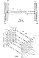
- Fig. 3 is a schematic diagram illustrating two-dimensional, free space optical link comprised of a two-dimensional transmitter array 302 and a two-dimensional receiver array 310.
- Transmitter array 302 is constructed of a plurality of multi-wavelength transmitter elements 304. Each multi-wavelength transmitter element broadcasts a multiplexed optical signal 306, comprising a number of channels at different wavelengths, through short haul, free space channel 308 to receiver array 310.
- Receiver array 310 is comprised of a corresponding number of filter/detector elements 312, each of which splits the multiplexed signal into several individual channels according to its wavelength.
- Fig. 4 shows the transmitter array of the invention.
- Two-dimensional transmitter array 302 comprises a set of collimating optics 408 and a corresponding set of vertical cavity surface emitting laser (VCSEL) arrays 410 that have been mounted to substrate 406, such as by a solder bond 402.
- VCSEL array 410 is a tightly bound structure of four VCSELs, each emitting an optical signal with a different wavelength. Either bottom-emitting or top-emitting VCSELs can be used for this application, but in this case, bottom-emitting VCSELs are preferred.
- bottom-emitting VCSELs allow the flip-chip solder bonding technique to be used to affix VCSEL array 410 onto substrate 406, which allows for convenient access to the contact pads for the VCSELs which are used to transmit the electrical data.
- the use of discrete VCSELs rather than a monolithic array of VCSELs reduces the thermal crosstalk between channels.
- Receiver array 310 comprises a plurality of filters 502 and a matching set of photodetectors 504 in arrangements that are affixed to substrate 508 by suitable means such as solder bond 510.
- Each filter element 502 and each photodetector element 504 comprises four electrically isolated segments designed to facilitate an optical signal of specified wavelength that has been broadcast through a short haul, free space channel from one of the transmitter arrays.
- Each segment of filter 502 has a filter element 512 that has been configured to select a specific signal having a particular wavelength.
- each photodetector 504 has a corresponding detector element 506 to detect one portion of the transmitted combined optical signal, thus isolating and converting only one optical signal having a specific wavelength.
- the filter may be thought of as a pie-shaped segment, as shown, of a partitioned filter. It may also be comprised of separate segments mounted together on the corresponding detector or on an optically transparent surface to which both the filters and the detectors are mounted.
- Transmitter array 302 comprises transmitter elements 304 (see Fig. 3), each having a tightly bound cluster of VCSELs 606 (shown as four in Fig. 4), each transmitting an optical signal at a different wavelength, and collimating optics 604.
- the collimating optics are designed to combine the optical signals emitted from each of the VCSELs into a single broadcasted signal 610 that is, in turn, transmitted through a short haul, free space channel 612 to receiver array 310.
- Positioning the emitters of each VCSEL 606 in a tight rectangular cluster and forcing the emitted signal through collimating optics allow multiple optical channels to be transmitted over a free space channel without the need of either an optical multiplexer or a demultiplexer.
- Receiver array 310 in Fig. 6 comprises tightly coupled sets of filter/detectors 312 comprised of multiple elements.
- Each filter/detector element consists of a tightly bound cluster of filters 616 and photodetecters 618.
- each filter 616 in the array passes the appropriate optical signal in accordance with an assigned wavelength, permitting the desired signal to be passed through to photodetector 618 while reflecting the rest.
- filter 616 is used as a wavelength-selecting device, only accepting the precise bandwidth of a specified optical signal, thus ensuring that each signal is properly selected.
- photodetector 618 converts the optical signal into an electrical signal for distribution through substrate 620 to a set of electronics 621, such as a receiver integrated circuit (IC), attached to backplane 622 that is able to transmit the converted signal to an appropriate receiver or source (not shown).
- a set of electronics 621 such as a receiver integrated circuit (IC)
- IC receiver integrated circuit
- backplane 622 that is able to transmit the converted signal to an appropriate receiver or source (not shown).
- substrate 620 is optional. It is possible that the filter/detector assemblies can be mounted directly to the receiver IC.
- Fig. 7 simply shows that the optical interconnection between transmitter 702 and receiver 706 may be through optical fibers 705. There is one fiber for each element of transmitter array 703 which transmits the signal through collimating optics 704. The signals are selected by filters 708 and detected by detectors 707 on receiver IC 706. The Fig. 7 version otherwise operates the same as the Fig. 6 apparatus.
- the free space distance may be between racks in a communication apparatus and could be as small a distance as physically practical, possibly 0.5 inch, and as distant as practical for line of sight coupling, possibly approximately one meter.
- the Fig. 7 embodiment, using optical fiber coupling could be any practical length and is not limited to line of sight.
- focusing optics may be employed on the receiver side of the apparatus of the invention, in addition to the collimating optics shown on the emitter side.
Landscapes
- Physics & Mathematics (AREA)
- Electromagnetism (AREA)
- Engineering & Computer Science (AREA)
- Computer Networks & Wireless Communication (AREA)
- Signal Processing (AREA)
- Optical Communication System (AREA)
- Optical Couplings Of Light Guides (AREA)
Abstract
Description
Claims (15)
- A two-dimensional free space optical link comprising:an array (302) of tightly-coupled, multi-wavelength arrays (410) of vertical cavity surface emitting lasers (VCSELs) (606), operating at predetermined wavelengths;collimating optics (408) for collimating the optical signals emitted from each said multi-wavelength array of VCSELs into a single uniform optical signal; andan array (310) of tightly-coupled optical receiver arrays (312), each said receiver array being configured to receive the signals from one of said VCSEL arrays, wherein the wavelengths of the received signals generally match the wavelengths of the signals transmitted by said VCSEL arrays such that multiple optical wavelengths can be simultaneously communicated at high-speed from one of said VCSEL arrays to one of said receiver arrays across a very short haul channel.
- The optical link recited in claim 1, wherein said VCSEL array is configured as a tightly-bound cluster of VCSELs.
- The optical link recited in claim 1 or 2, wherein the emitting elements of each VCSEL in said cluster form a small group positioned at the focal point of said collimating optics.
- The optical link recited in one of the preceding claims, wherein said tightly-coupled optical receiver array of the said receiver arrays comprise partitioned optical filters (502) and mating photodetectors (504).
- The optical link recited in claim 4, wherein said optical filters of each said optical receiver array further comprise multiple segments (616), each segment having an individual filter element designed to pass a transmitted optical signal with a specific wavelength range.
- The optical link recited in claim 4 or 5, wherein said photodetectors of each said optical receiver array further comprise multiple segments (618), each segment having an individual photodetector element that converts the transmitted optical signal received from each said filter element to an electrical signal.
- The optical link recited in one of the preceding claims, wherein said short' haul channel is free space.
- The optical link recited in one of the preceding claims, wherein said short haul channel is optical fibers (705).
- A method of creating a two-dimensional optical link, the method comprising:assembling a vertical cavity surface emitting laser (VCSEL) emitter array (302), wherein the VCSEL emitters (606) in the array are arranged in a regular pattern and each VCSEL emitter is set for a different emissive wavelength;fabricating a receiver array (310), wherein the receiver array comprises a plurality of optical filters (502) and mating photodetector arrangements (504); andmounting the VCSEL emitter array and receiver array onto respective transmitter and receiver electronic circuits configured to receive the respective emitter and receiver arrays.
- The method recited in claim 9, wherein each optical filter and photodetector arrangement has a plurality of segments (616, 618), each segment having an individual filter and a mating photodector element where each filter is configured to pass one wavelength and each photodetector converts a specific optical signal with a specified wavelength to an electrical signal.
- The method recited in claim 9 or 10, and further comprising transmitting signals from the emitter array to the receiver array through free space.
- The method recited in claim 9, 10 or 11, and further comprising transmitting signals from the emitter array to the receiver array through optical fibers (705).
- A two-dimensional optical link comprising:an array (302) of tightly-coupled, multi-wavelength arrays (410) of vertical cavity surface emitting lasers (VCSELs) (606), transmitting signals at predetermined wavelengths;collimating optics (408) for collimating the optical signals emitted from each said multi-wavelength array of VCSELs into a single uniform optical signal; andan array (310) of tightly coupled optical receiver arrays (312), each said receiver array being configured to receive a signal from one of said VCSEL arrays, wherein the wavelengths of the signals received from said VCSEL arrays generally match the wavelengths of the signals transmitted by said VCSEL arrays such that multiple optical wavelengths can be simultaneously communicated at high-speed from said VCSEL arrays to said receiver arrays across a channel.
- The optical link recited in claim 13, wherein the signals from said VCSEL arrays are transmitted across the channel, to said receiver arrays through free space.
- The optical link recited in claim 13, wherein the signals from said VCSEL arrays are transmitted across the channel to said receiver arrays through optical fibers (705).
Applications Claiming Priority (2)
| Application Number | Priority Date | Filing Date | Title |
|---|---|---|---|
| US80944 | 2002-02-22 | ||
| US10/080,944 US7978981B2 (en) | 2002-02-22 | 2002-02-22 | Structure and apparatus for a very short haul, free space, and fiber optic interconnect and data link |
Publications (3)
| Publication Number | Publication Date |
|---|---|
| EP1345340A2 true EP1345340A2 (en) | 2003-09-17 |
| EP1345340A3 EP1345340A3 (en) | 2004-11-17 |
| EP1345340B1 EP1345340B1 (en) | 2009-01-28 |
Family
ID=27765248
Family Applications (1)
| Application Number | Title | Priority Date | Filing Date |
|---|---|---|---|
| EP02022781A Expired - Lifetime EP1345340B1 (en) | 2002-02-22 | 2002-10-11 | Structure and apparatus for a very short haul, free space interconnect and data link |
Country Status (3)
| Country | Link |
|---|---|
| US (1) | US7978981B2 (en) |
| EP (1) | EP1345340B1 (en) |
| DE (2) | DE20221906U1 (en) |
Cited By (2)
| Publication number | Priority date | Publication date | Assignee | Title |
|---|---|---|---|---|
| EP1507344A3 (en) * | 2003-08-13 | 2005-09-07 | Northrop Grumman Corporation | Free space optical bus |
| EA008528B1 (en) * | 2005-06-10 | 2007-06-29 | Фонд Сопровождения Инвестиционных Проектов "Генкей" | Method and device for transmitting digital information |
Families Citing this family (25)
| Publication number | Priority date | Publication date | Assignee | Title |
|---|---|---|---|---|
| US7978981B2 (en) * | 2002-02-22 | 2011-07-12 | Avago Technologies Fiber Ip (Singapore) Pte. Ltd. | Structure and apparatus for a very short haul, free space, and fiber optic interconnect and data link |
| US20070127926A1 (en) * | 2003-11-17 | 2007-06-07 | Fabio Marioni | Free space optical conditioner |
| US7680417B2 (en) * | 2005-12-28 | 2010-03-16 | Intel Corporation | Bi-directional parallel optical link |
| JP5031427B2 (en) * | 2007-03-30 | 2012-09-19 | 三星電子株式会社 | Visible light transmitter, visible light receiver, visible light communication system, and visible light communication method |
| US7929865B2 (en) * | 2007-07-27 | 2011-04-19 | Hewlett-Packard Development Company, L.P. | Free space WDM signal detector |
| US8417124B2 (en) * | 2008-11-05 | 2013-04-09 | Broadcom Corporation | Multiple input, multiple output (MIMO) communication via multimode media |
| US10038304B2 (en) | 2009-02-17 | 2018-07-31 | Trilumina Corp. | Laser arrays for variable optical properties |
| US20130223846A1 (en) | 2009-02-17 | 2013-08-29 | Trilumina Corporation | High speed free-space optical communications |
| US8995493B2 (en) | 2009-02-17 | 2015-03-31 | Trilumina Corp. | Microlenses for multibeam arrays of optoelectronic devices for high frequency operation |
| US8995485B2 (en) | 2009-02-17 | 2015-03-31 | Trilumina Corp. | High brightness pulsed VCSEL sources |
| US10244181B2 (en) | 2009-02-17 | 2019-03-26 | Trilumina Corp. | Compact multi-zone infrared laser illuminator |
| US11095365B2 (en) | 2011-08-26 | 2021-08-17 | Lumentum Operations Llc | Wide-angle illuminator module |
| US9160450B2 (en) * | 2011-09-23 | 2015-10-13 | Te Connectivity Nederland B.V. | Multi-channel transceiver |
| US11194224B2 (en) * | 2013-03-15 | 2021-12-07 | Wavefront Research, Inc. | Low power compact optical communication and collision avoidance systems |
| US11726384B1 (en) * | 2013-03-15 | 2023-08-15 | Wavefront Research, Inc. | Low power compact optical communication and collision avoidance systems |
| US10411812B1 (en) * | 2013-03-15 | 2019-09-10 | Forrest Rose | Optical interconnect computing module tolerant to changes in position and orientation |
| JP6339665B2 (en) * | 2013-04-22 | 2018-06-06 | トリルミナ コーポレーション | Microlens for optoelectronic multi-beam array for high frequency operation |
| CN105874662B (en) * | 2013-04-22 | 2019-02-22 | 三流明公司 | Microlenses for multi-beam arrays of optoelectronic devices operating at high frequencies |
| EP3017555B1 (en) * | 2013-07-01 | 2020-10-28 | Nokia Technologies Oy | Directional optical communications |
| JP5991697B2 (en) * | 2013-12-19 | 2016-09-14 | インターナショナル・ビジネス・マシーンズ・コーポレーションInternational Business Machines Corporation | Optical connection apparatus, information processing apparatus, and data transmission method |
| US9800332B2 (en) * | 2013-12-27 | 2017-10-24 | Space Photonics, Inc. | Acquisition, tracking, and pointing apparatus for free space optical communications with moving focal plane array |
| EP2985636B1 (en) * | 2014-08-11 | 2018-07-25 | Leuze electronic GmbH + Co KG | Method for aligning a sensor device |
| CN108008501B (en) * | 2016-11-01 | 2021-10-29 | 住友电工光电子器件创新株式会社 | Optical transmitter apparatus |
| US10263700B2 (en) * | 2017-09-21 | 2019-04-16 | David Lynn | Panels with Li-Fi connectivity |
| CN110470224B (en) * | 2019-09-16 | 2024-05-28 | 广州贝晓德智能科技有限公司 | Panoramic scanning multipoint detection sensor |
Family Cites Families (69)
| Publication number | Priority date | Publication date | Assignee | Title |
|---|---|---|---|---|
| US3573433A (en) * | 1968-01-15 | 1971-04-06 | Ibm | Optical read-only memory |
| US3633035A (en) * | 1968-11-16 | 1972-01-04 | Nippon Selfoc Co Ltd | Multiplexed optical communications system |
| FR2122007A5 (en) * | 1971-01-14 | 1972-08-25 | Thomson Csf | |
| FR2293035A1 (en) * | 1974-11-26 | 1976-06-25 | Thomson Csf | SYSTEM FOR READING OPTICAL BINARY DIGITAL DATA RECORDING |
| FR2520960B1 (en) * | 1982-02-03 | 1986-12-12 | Rozenwaig Boris | IMPROVEMENTS ON MULTI-CELL RECEIVERS OPTO-ELECTRIC SWITCHES |
| US4651297A (en) * | 1984-11-28 | 1987-03-17 | General Dynamics, Pomona Division | Two-dimensional image correlator |
| US4705344A (en) * | 1984-12-19 | 1987-11-10 | American Telephone And Telegraph Company, At&T Bell Laboratories | Optical interconnection arrangement |
| US4641273A (en) * | 1985-03-15 | 1987-02-03 | Teledyne Industries, Inc. | General time, space and frequency multiplexed acousto-optic correlator |
| US4939630A (en) * | 1986-09-09 | 1990-07-03 | Nikon Corporation | Illumination optical apparatus |
| US5078499A (en) * | 1989-08-04 | 1992-01-07 | At&T Bell Laboratories | Optical interconnection arrangement |
| US5333077A (en) * | 1989-10-31 | 1994-07-26 | Massachusetts Inst Technology | Method and apparatus for efficient concentration of light from laser diode arrays |
| US5081637A (en) * | 1989-11-28 | 1992-01-14 | Massachusetts Institute Of Technology | Multiple-laser pump optical system |
| US5093879A (en) * | 1990-06-22 | 1992-03-03 | International Business Machines Corporation | Electro-optical connectors |
| CH682698A5 (en) * | 1990-11-01 | 1993-10-29 | Fisba Optik Ag Bystronic Laser | Method in which several, arranged in one or more rows of radiation sources are imaged and apparatus therefor. |
| US5291324A (en) * | 1992-11-24 | 1994-03-01 | At&T Bell Laboratories | Comparison apparatus with freespace optical interconnections between optoelectronic integrated circuits |
| US5513201A (en) * | 1993-04-30 | 1996-04-30 | Nippon Steel Corporation | Optical path rotating device used with linear array laser diode and laser apparatus applied therewith |
| US5546209A (en) * | 1994-03-11 | 1996-08-13 | University Of Southern California | One-to-many simultaneous and reconfigurable optical two-dimensional plane interconnections using multiple wavelength, vertical cavity, surface-emitting lasers and wavelength-dependent detector planes |
| US5557693A (en) * | 1994-10-21 | 1996-09-17 | Unisys Corporation | Apparatus and method for transmitting optical data |
| US5650612A (en) * | 1995-01-11 | 1997-07-22 | The Boeing Company | Optical sensor using swept wavelength light source |
| DE19514626C2 (en) * | 1995-04-26 | 1997-03-06 | Fraunhofer Ges Forschung | Arrangement for shaping the geometric cross section of a radiation field of one or more solid-state and / or semiconductor lasers |
| JPH0973041A (en) * | 1995-06-26 | 1997-03-18 | Oki Electric Ind Co Ltd | Microoptical system for free space optical wiring and its setting |
| JPH09138712A (en) * | 1995-08-29 | 1997-05-27 | Nec Corp | Mutually connected network |
| US5781671A (en) * | 1995-10-04 | 1998-07-14 | Nec Research Institute, Inc. | Free-space angle-multiplexed optical interconnect network |
| EP0811862B1 (en) * | 1996-06-03 | 2004-08-25 | Nippon Telegraph And Telephone Corporation | Board-to-board and unit-to-unit optical interconnection system |
| US5914976A (en) | 1997-01-08 | 1999-06-22 | W. L. Gore & Associates, Inc. | VCSEL-based multi-wavelength transmitter and receiver modules for serial and parallel optical links |
| US5900981A (en) * | 1997-04-15 | 1999-05-04 | Scitex Corporation Ltd. | Optical system for illuminating a spatial light modulator |
| US5857042A (en) * | 1997-04-29 | 1999-01-05 | Mcgill University | Optical interconnection arrangements |
| US6044096A (en) * | 1997-11-03 | 2000-03-28 | Sdl, Inc. | Packaged laser diode array system and method with reduced asymmetry |
| KR100276968B1 (en) * | 1998-07-11 | 2001-01-15 | 윤덕용 | Optical interconnection structure for enlarging alignment tolerance |
| DE19839902C1 (en) * | 1998-09-02 | 2000-05-25 | Laserline Ges Fuer Entwicklung | Optical arrangement for use in a laser diode arrangement and diode laser |
| US6775480B1 (en) * | 1998-09-10 | 2004-08-10 | Nortel Networks Limited | Free space optical interconnect system |
| CA2308390A1 (en) | 1998-09-10 | 2000-03-23 | Nortel Networks Corporation | Free space optical interconnect system |
| US6215598B1 (en) * | 1998-10-05 | 2001-04-10 | Ruey Jennifer Hwu | Apparatus and method for concentrating beams from broad area diode lasers, diode laser bars and/ or diode laser arrays |
| US7446298B1 (en) * | 1998-10-22 | 2008-11-04 | Wavefront Research, Inc. | Relaxed tolerance optical interconnect systems |
| US6195485B1 (en) | 1998-10-26 | 2001-02-27 | The Regents Of The University Of California | Direct-coupled multimode WDM optical data links with monolithically-integrated multiple-channel VCSEL and photodetector |
| US6005717A (en) * | 1998-11-17 | 1999-12-21 | Ceramoptec Industries, Inc. | Diode laser beam combiner system |
| US6091537A (en) * | 1998-12-11 | 2000-07-18 | Xerox Corporation | Electro-actuated microlens assemblies |
| EP1175742A1 (en) * | 1999-02-11 | 2002-01-30 | QuantumBeam Limited | Optical free space signalling system |
| JP2002541513A (en) * | 1999-03-31 | 2002-12-03 | フラウンホッファー−ゲゼルシャフト ツァ フェルダールング デァ アンゲヴァンテン フォアシュンク エー.ファオ. | Optical array for symmetrical illumination of a two-dimensional array of laser diodes |
| US6486984B1 (en) * | 1999-06-07 | 2002-11-26 | Agilent Technologies, Inc. | Wavelength monitor using hybrid approach |
| US6326600B1 (en) * | 1999-06-21 | 2001-12-04 | Applied Photonics, Inc. | Method and apparatus for distortion reduction in optoelectronic interconnections |
| US6356577B1 (en) * | 1999-07-15 | 2002-03-12 | Silicon Light Machines | Method and apparatus for combining light output from multiple laser diode bars |
| DE19939750C2 (en) * | 1999-08-21 | 2001-08-23 | Laserline Ges Fuer Entwicklung | Optical arrangement for use in a laser diode arrangement and laser diode arrangement with such an optical arrangement |
| US6889010B2 (en) * | 1999-09-03 | 2005-05-03 | Altera Corporation | Star topology network with fiber interconnect on chip |
| US6434308B1 (en) * | 1999-09-03 | 2002-08-13 | Teraconnect, Inc | Optoelectronic connector system |
| US6509992B1 (en) * | 1999-09-09 | 2003-01-21 | Nortel Networks Corporation | Free space optical interconnect system tolerant to misalignments and method of operation thereof |
| US6583904B1 (en) * | 1999-10-01 | 2003-06-24 | Eci Telecom Ltd. | Method and apparatus for aligning optical interconnections between printed circuit boards |
| US6527456B1 (en) * | 1999-10-13 | 2003-03-04 | Teraconnect, Inc. | Cluster integration approach to optical transceiver arrays and fiber bundles |
| US6117193A (en) * | 1999-10-20 | 2000-09-12 | Amkor Technology, Inc. | Optical sensor array mounting and alignment |
| US7020400B2 (en) | 1999-12-24 | 2006-03-28 | Altera Corporation | Multi-wavelength optical communication system |
| GB0000908D0 (en) * | 2000-01-14 | 2000-03-08 | Scient Generics Ltd | Parallel free-space optical communications |
| US6400513B1 (en) * | 2000-03-15 | 2002-06-04 | Quantum Devices, Inc. | Optical beam coupling of multiple wavelengths into an output channel using spatial wavefront segmentation |
| US6530700B2 (en) * | 2000-04-21 | 2003-03-11 | Teraconnect, Inc. | Fiber optic connector |
| US6367989B1 (en) * | 2000-05-22 | 2002-04-09 | Motorola, Inc. | Optical interconnect method and apparatus |
| US6545425B2 (en) * | 2000-05-26 | 2003-04-08 | Exaconnect Corp. | Use of a free space electron switch in a telecommunications network |
| US6353502B1 (en) * | 2000-06-13 | 2002-03-05 | Eastman Kodak Company | VCSEL field correction |
| US6450694B1 (en) | 2000-06-20 | 2002-09-17 | Corona Optical Systems, Inc. | Dynamically configurable backplane |
| US6556352B2 (en) * | 2000-08-23 | 2003-04-29 | Apollo Instruments Inc. | Optical coupling system |
| AU2002211875A1 (en) * | 2000-10-06 | 2002-04-15 | Bae Systems Information And Electronic Sytems Integration Inc. | Optical fiber utilization for vcsel driven communications |
| US6493148B1 (en) * | 2000-11-08 | 2002-12-10 | Opto Power Corporation | Increasing laser beam power density |
| US6516011B1 (en) * | 2000-11-08 | 2003-02-04 | Opto-Power Corp. | Focusing multiple laser beams |
| US6666590B2 (en) * | 2000-12-14 | 2003-12-23 | Northrop Grumman Corporation | High brightness laser diode coupling to multimode optical fibers |
| US6909554B2 (en) * | 2000-12-27 | 2005-06-21 | Finisar Corporation | Wafer integration of micro-optics |
| US6853812B2 (en) * | 2001-05-09 | 2005-02-08 | Robert Mays, Jr. | Polarized-holographic filtering providing improved extinction ratio |
| US6775308B2 (en) * | 2001-06-29 | 2004-08-10 | Xanoptix, Inc. | Multi-wavelength semiconductor laser arrays and applications thereof |
| US6591042B2 (en) * | 2001-10-10 | 2003-07-08 | Schott Optovance, Inc. | Fiber based wavelength de-multiplexing system |
| US7155129B2 (en) * | 2002-01-07 | 2006-12-26 | Xerox Corporation | Steerable free space optical interconnect apparatus |
| US7978981B2 (en) * | 2002-02-22 | 2011-07-12 | Avago Technologies Fiber Ip (Singapore) Pte. Ltd. | Structure and apparatus for a very short haul, free space, and fiber optic interconnect and data link |
| US7116694B2 (en) * | 2002-12-11 | 2006-10-03 | Avago Technologies Fiber Ip (Singapore) Pte. Ltd. | Transmitter array with pixel element that has primary semiconductor laser and at least one secondary semiconductor laser |
-
2002
- 2002-02-22 US US10/080,944 patent/US7978981B2/en not_active Expired - Fee Related
- 2002-10-11 EP EP02022781A patent/EP1345340B1/en not_active Expired - Lifetime
- 2002-10-11 DE DE20221906U patent/DE20221906U1/en not_active Expired - Lifetime
- 2002-10-11 DE DE60231026T patent/DE60231026D1/en not_active Expired - Lifetime
Cited By (3)
| Publication number | Priority date | Publication date | Assignee | Title |
|---|---|---|---|---|
| EP1507344A3 (en) * | 2003-08-13 | 2005-09-07 | Northrop Grumman Corporation | Free space optical bus |
| US7403715B2 (en) | 2003-08-13 | 2008-07-22 | Northrop Grumman Corporation | Free space optical bus |
| EA008528B1 (en) * | 2005-06-10 | 2007-06-29 | Фонд Сопровождения Инвестиционных Проектов "Генкей" | Method and device for transmitting digital information |
Also Published As
| Publication number | Publication date |
|---|---|
| US20040207926A1 (en) | 2004-10-21 |
| DE20221906U1 (en) | 2009-01-15 |
| EP1345340B1 (en) | 2009-01-28 |
| US7978981B2 (en) | 2011-07-12 |
| EP1345340A3 (en) | 2004-11-17 |
| DE60231026D1 (en) | 2009-03-19 |
Similar Documents
| Publication | Publication Date | Title |
|---|---|---|
| US7978981B2 (en) | Structure and apparatus for a very short haul, free space, and fiber optic interconnect and data link | |
| KR101624404B1 (en) | Replaceable transmitting module and optical transceiver having the same | |
| US5896213A (en) | Optical fiber network system | |
| US9306671B2 (en) | Thermally isolated multi-channel transmitter optical subassembly and optical transceiver module including same | |
| US9703054B2 (en) | Aligning and directly optically coupling photodetectors to optical demultiplexer outputs in a multichannel receiver optical subassembly | |
| US20140029943A1 (en) | Coplanar routing for optical transmission | |
| US9847434B2 (en) | Multichannel receiver optical subassembly with improved sensitivity | |
| US20050036789A1 (en) | Free space optical bus | |
| US6243175B1 (en) | WDM optical communication system having reduced loss and cross-talk | |
| US11303379B1 (en) | Communication between data centers using a multi-core fiber | |
| US6928247B2 (en) | WDM ring transmission system | |
| US20030185502A1 (en) | Optical receiving apparatus, optical transmitting apparatus, optical transmitting/receiving apparatus and optical transfer system | |
| US20160291267A1 (en) | Coupling of photodetector array to optical demultiplexer outputs with index matched material | |
| CN1737619B (en) | Optical duplexer and optical triplexer | |
| US7352967B1 (en) | Data transmission system | |
| US20050074203A1 (en) | Device for multiplexing an array of optical channels, use for wavelength and add-drop multiplexing | |
| EP1294118B1 (en) | Data transmission system | |
| EP3075082B1 (en) | Photodetectors aligning and coupling optical demultiplexer outputs | |
| US20260067019A1 (en) | Optical receiving device and optical module | |
| US6694101B1 (en) | Focal plane division multiplexing system and method | |
| CA2289320A1 (en) | Integrating optical adm filters | |
| KR100347127B1 (en) | Method for optical multiplexing and system for performming the same | |
| JPS6253031A (en) | Wavelength multiplex optical fiber transmission system | |
| KR19990068254A (en) | Multipath Optical Multiplexer | |
| KR20060064489A (en) | Broadcast signal transmission method and passive optical subscriber network system in passive optical subscriber network system |
Legal Events
| Date | Code | Title | Description |
|---|---|---|---|
| PUAI | Public reference made under article 153(3) epc to a published international application that has entered the european phase |
Free format text: ORIGINAL CODE: 0009012 |
|
| AK | Designated contracting states |
Kind code of ref document: A2 Designated state(s): AT BE BG CH CY CZ DE DK EE ES FI FR GB GR IE IT LI LU MC NL PT SE SK TR |
|
| AX | Request for extension of the european patent |
Extension state: AL LT LV MK RO SI |
|
| PUAL | Search report despatched |
Free format text: ORIGINAL CODE: 0009013 |
|
| AK | Designated contracting states |
Kind code of ref document: A3 Designated state(s): AT BE BG CH CY CZ DE DK EE ES FI FR GB GR IE IT LI LU MC NL PT SE SK TR |
|
| AX | Request for extension of the european patent |
Extension state: AL LT LV MK RO SI |
|
| 17P | Request for examination filed |
Effective date: 20050418 |
|
| AKX | Designation fees paid |
Designated state(s): DE FR GB |
|
| RAP1 | Party data changed (applicant data changed or rights of an application transferred) |
Owner name: AVAGO TECHNOLOGIES FIBER IP (SINGAPORE) PTE. LTD. |
|
| GRAP | Despatch of communication of intention to grant a patent |
Free format text: ORIGINAL CODE: EPIDOSNIGR1 |
|
| RTI1 | Title (correction) |
Free format text: STRUCTURE AND APPARATUS FOR A VERY SHORT HAUL, FREE SPACE INTERCONNECT AND DATA LINK |
|
| GRAS | Grant fee paid |
Free format text: ORIGINAL CODE: EPIDOSNIGR3 |
|
| GRAA | (expected) grant |
Free format text: ORIGINAL CODE: 0009210 |
|
| AK | Designated contracting states |
Kind code of ref document: B1 Designated state(s): DE FR GB |
|
| REG | Reference to a national code |
Ref country code: GB Ref legal event code: FG4D |
|
| REF | Corresponds to: |
Ref document number: 60231026 Country of ref document: DE Date of ref document: 20090319 Kind code of ref document: P |
|
| PLBE | No opposition filed within time limit |
Free format text: ORIGINAL CODE: 0009261 |
|
| STAA | Information on the status of an ep patent application or granted ep patent |
Free format text: STATUS: NO OPPOSITION FILED WITHIN TIME LIMIT |
|
| 26N | No opposition filed |
Effective date: 20091029 |
|
| REG | Reference to a national code |
Ref country code: FR Ref legal event code: ST Effective date: 20100630 |
|
| PG25 | Lapsed in a contracting state [announced via postgrant information from national office to epo] |
Ref country code: FR Free format text: LAPSE BECAUSE OF NON-PAYMENT OF DUE FEES Effective date: 20091102 |
|
| PG25 | Lapsed in a contracting state [announced via postgrant information from national office to epo] |
Ref country code: GB Free format text: LAPSE BECAUSE OF NON-PAYMENT OF DUE FEES Effective date: 20091011 |
|
| REG | Reference to a national code |
Ref country code: DE Ref legal event code: R082 Ref document number: 60231026 Country of ref document: DE Representative=s name: DILG HAEUSLER SCHINDELMANN PATENTANWALTSGESELL, DE |
|
| REG | Reference to a national code |
Ref country code: DE Ref legal event code: R082 Ref document number: 60231026 Country of ref document: DE Representative=s name: DILG HAEUSLER SCHINDELMANN PATENTANWALTSGESELL, DE Effective date: 20130701 Ref country code: DE Ref legal event code: R081 Ref document number: 60231026 Country of ref document: DE Owner name: AVAGO TECHNOLOGIES GENERAL IP (SINGAPORE) PTE., SG Free format text: FORMER OWNER: AVAGO TECHNOLOGIES FIBER IP (SINGAPORE) PTE. LTD., SINGAPORE, SG Effective date: 20130701 |
|
| PGFP | Annual fee paid to national office [announced via postgrant information from national office to epo] |
Ref country code: DE Payment date: 20150922 Year of fee payment: 14 |
|
| REG | Reference to a national code |
Ref country code: DE Ref legal event code: R119 Ref document number: 60231026 Country of ref document: DE |
|
| PG25 | Lapsed in a contracting state [announced via postgrant information from national office to epo] |
Ref country code: DE Free format text: LAPSE BECAUSE OF NON-PAYMENT OF DUE FEES Effective date: 20170503 |