EP1345237A2 - High voltage generation and regulation system for digital multilevel nonvolatile memory - Google Patents
High voltage generation and regulation system for digital multilevel nonvolatile memory Download PDFInfo
- Publication number
- EP1345237A2 EP1345237A2 EP03250092A EP03250092A EP1345237A2 EP 1345237 A2 EP1345237 A2 EP 1345237A2 EP 03250092 A EP03250092 A EP 03250092A EP 03250092 A EP03250092 A EP 03250092A EP 1345237 A2 EP1345237 A2 EP 1345237A2
- Authority
- EP
- European Patent Office
- Prior art keywords
- voltage
- terminal
- signal
- coupled
- output
- Prior art date
- Legal status (The legal status is an assumption and is not a legal conclusion. Google has not performed a legal analysis and makes no representation as to the accuracy of the status listed.)
- Withdrawn
Links
Images



Classifications
-
- H—ELECTRICITY
- H02—GENERATION; CONVERSION OR DISTRIBUTION OF ELECTRIC POWER
- H02M—APPARATUS FOR CONVERSION BETWEEN AC AND AC, BETWEEN AC AND DC, OR BETWEEN DC AND DC, AND FOR USE WITH MAINS OR SIMILAR POWER SUPPLY SYSTEMS; CONVERSION OF DC OR AC INPUT POWER INTO SURGE OUTPUT POWER; CONTROL OR REGULATION THEREOF
- H02M3/00—Conversion of DC power input into DC power output
- H02M3/02—Conversion of DC power input into DC power output without intermediate conversion into AC
- H02M3/04—Conversion of DC power input into DC power output without intermediate conversion into AC by static converters
- H02M3/06—Conversion of DC power input into DC power output without intermediate conversion into AC by static converters using resistors or capacitors, e.g. potential divider
- H02M3/07—Conversion of DC power input into DC power output without intermediate conversion into AC by static converters using resistors or capacitors, e.g. potential divider using capacitors charged and discharged alternately by semiconductor devices with control electrode, e.g. charge pumps
-
- G—PHYSICS
- G11—INFORMATION STORAGE
- G11C—STATIC STORES
- G11C16/00—Erasable programmable read-only memories
- G11C16/02—Erasable programmable read-only memories electrically programmable
- G11C16/06—Auxiliary circuits, e.g. for writing into memory
- G11C16/30—Power supply circuits
Definitions
- the invention relates to a high voltage signal generator and regulator, and more particularly to a high voltage signal generator and regulator for a memory, such as a digital multilevel nonvolatile memory.
- a conventional mixed mode integrated circuit system frequently uses different voltage supplies.
- Analog signal processing such as amplification, comparison, pulse generation, may be performed at high voltage.
- a FLASH memory applies an erase signal and a program signal to memory cells.
- the erase signal and the program signal have voltage levels greater than a supply voltage. Also in multilevel volatile memories, the variation of the voltage level of the program signal falls in a smaller range for the multibit signals stored in the memory cells.
- the present invention provides a high voltage generation and regulation system that generates at least one voltage signal having a voltage level greater than the supply voltage.
- the system may comprise a charge pump, a loop regulator, and a nested loop regulator.
- the charge pump may comprise at least one pump and an oscillator.
- the oscillator provides clock signals to the at least one pump.
- the output of the oscillator may be disabled without turning off the clock generation.
- the oscillator may be a ring oscillator.
- the ring oscillator and the output stage may comprise inverters with a capacitor coupled to the output of the inverter.
- the ratio of the capacitors in the ring oscillator to the capacitor in the output stage determine the phase shift between the two clock signals.
- the capacitance of the capacitors are identical and a bias applied the ring oscillator and the output stage are ratioed to adjust the phase between the two clock signals.
- the pump may include a plurality of voltage boost stages coupled in series.
- Each voltage boost stage generates an output signal having a voltage level higher than an input voltage applied thereto and comprises a first transistor coupled between the input of voltage and an output voltage, and a power-up assist diode to charge the input voltage applied to the voltage boost stage coupled to the output signal.
- the power-up assist diode also operates for forward VT (threshold voltage) canceling.
- the voltage boost stage may include a backward VT cancellation transistor coupled to the first transistor to substantially cancel threshold voltage of the first transistor in response to the output signal.
- the voltage boost stage may include a high voltage self-biasing circuit to precharge the output signal of the voltage boost stage.
- the regulator may comprise a voltage regulator providing a regulated voltage signal in response to an input voltage signal and a control signal, a comparator coupled to the voltage regulator to generate the control signal in response to the regulated voltage signal, and a slew rate enhancement circuit coupled to an output of the comparator to boost the control signal in the event a regulated voltage signal has a voltage level less than a threshold voltage.
- the slew rate enhancement circuit may include a source follower, and may include a voltage divider that provides a divided signal to the comparator in response to the regulated voltage signal.
- the nested loop regulator monitors the regulated voltage signal and disables the oscillator outputs when the voltage of the regulated voltage signal is substantially identical to a predetermined value.
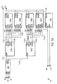
- Figure 1 is a block diagram illustrating a high voltage generation and regulation system in accordance with the present invention.
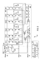
- Figure 1a is a block diagram illustrating a charge pump of the high voltage generation and regulation system of Figure 1.
- Figure 2 is a schematic diagram of an oscillator of the charge pump of Figure 1a.
- Figure 3 is a schematic diagram of a phase driver of the charge pump of Figure 1a.
- Figure 4 is a schematic diagram illustrating a phase buffer of the phase driver of Figure 3.
- Figure 5 is a schematic diagram illustrating a pump of the charge pump of Figure 1a.
- Figure 6 is a schematic diagram illustrating an initial voltage boost stage circuit of the pump of Figure 5.
- Figure 7 is a schematic diagram illustrating an intermediate voltage boost stage circuit of the pump of Figure 5.
- Figure 8 is a schematic diagram illustrating a final voltage boost stage circuit of the pump of Figure 5.
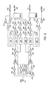
- Figure 9 is a schematic diagram illustrating a pump regulator of the high voltage generation and regulation system of Figure 1.
- FIG. 10 is a schematic diagram illustrating a high medium supply (VHMSUP) voltage regulator of the pump regulator of Figure 9.
- VHMSUP high medium supply
- FIG 11 is a schematic diagram illustrating an output boost circuit of the high medium supply (VHMSUP) voltage regulator of Figure 10.
- VHMSUP high medium supply
- Figure 12 is a schematic diagram illustrating a feedback voltage divider of the voltage regulator of Figure 10.
- Figure 13 is a schematic diagram illustrating a voltage divider multiplexer of the feedback voltage divider of Figure 12.
- Figure 14 is a schematic diagram illustrating a loop regulator of the high voltage generator and regulation system of Figure 1.
- Figure 15 is a schematic diagram illustrating a medium voltage pump generator of the charge pump of Figure 1a.
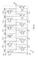
- Figure 16 is a schematic diagram illustrating a medium voltage pump voltage divider of the medium voltage pump generator of Figure 15.
- FIG. 1 is a block diagram illustrating a high voltage generation and regulation system 10 in accordance with the present invention.
- the high voltage generation and regulation system 10 generates a plurality of regulated power signals having different voltage levels and at voltage levels greater than a supply voltage applied to the system 10.
- the high voltage generation and regulation system 10 uses slew rate enhancement for decreased power up time.
- the high voltage generation and regulation system 10 includes nested loop regulation to achieve optimal power efficiency and high precision.
- the high voltage generation and regulation system 10 provides the plurality of regulated power signals to a memory device (not shown).
- the memory device is a digital multilevel nonvolatile memory.
- the high voltage generation and regulation system 10 comprises a charge pump 12, a pump regulator 14, and a loop regulator 16.
- the charge pump 12 generates a high voltage pump (VHPUMP) signal 20 and an oscillator test (POSC) signal 22.
- the high voltage pump (VHPUMP) signal 20 is enabled in response to an enable signal (ENB) 28 from the loop regulator 16.
- ENB is enable bar, which is indicative of an active low signal.
- the oscillator test signal 22 provides a test signal to analyze the output of an oscillator 102 (see Figure 1a) in the charge pump 12 or may be used as an input port to force an oscillator signal into the charge pump 12.
- a power down (PDB) signal 26 turns off the charge pump 12.
- a first reference (IREFN1) signal 24 from a band gap voltage circuit provides a reference current to the charge pump 12 to adjust the bias of the oscillator 102 (see Figure 1a).
- Band gap voltage circuits used in charge pump circuits and memory devices are well known in the art.
- a medium voltage pump (VMPUMP) signal 30 from the pump regulator 14 provides a self bias high voltage level for the charge pump 12.
- the pump regulator 14 generates a plurality of regulated power signals having different voltage levels. Specifically, the pump regulator 14 generates a high voltage supply (VHSUP) signal 40, a medium high voltage supply (VHMSUP) signal 42, the medium voltage pump (VMPUMP) signal 30 and a medium voltage supply (VMSUP) signal 44 in response to the high voltage pump (VHPUMP) signal 20 from the charge pump 12.
- VHSUP high voltage supply
- VHMSUP medium high voltage supply
- VMPUMP medium voltage pump
- VMSUP medium voltage supply
- VHPUMP medium voltage supply
- a reference voltage (VREF) signal 32 sets a reference for regulating the high voltage (VHSUP) signal 40 and the medium high voltage pump (VHMSUP) signal 42.
- a second reference (IREFN2) signal 46 controls the biasing of the pump regulator 14.
- a voltage divider disable (DISVIDB) signal 48 forms an enable/disable signal for the pump regulator 14.
- a plurality of voltage selection signals are applied to the pump regulator 14 for setting a divided voltage as a reference voltage for the pump regulator 14.
- a first voltage selection (FVHMSUP0) signal 50 a second voltage selection (FVHMSUP1) signal 52, a third voltage selection (FVHMSUP2) signal 54, and a fourth voltage selection (FVHMSUP3) signal 56 set a multiplexer 1204 (see Figure 12) to change the voltages of a voltage divider 1006 (see Figure 10) to adjust the reference voltage applied to an operational amplifier 1008 (see Figure 10).
- the power down (PD) signal 38 disables the pump regulator 14 during power down.
- the loop regulator 16 provides nested loop regulation to control the charge pump 12.
- the loop regulator 16 generates the enable (ENB) signal 28 to disable the charge pump 12 in response to the high voltage pump (VHPUMP) signal 20 being above a certain threshold and the enable (EN) signal 36.
- the reference voltage (VREF) signal 32 sets a trigger voltage for comparing to the high voltage pump (VHPUMP) signal 20 in the loop regulator 16 to set the enable (ENB) signal 28.
- a third reference (IREFN3) signal 34 from a band gap voltage circuit (not shown) controls the biasing of an operational amplifier 1404 (see Figure 14) of the loop regulator 16.
- the power down (PD) signal 38 disables the loop regulator 16 during power down.
- FIG. 1a is a block diagram illustrating the charge pump 12, which comprises an oscillator 102, a plurality of phase drivers 104-1 and 104-2, a plurality of pumps 106-1, 106-2, 106-3, and 106-4, and a medium voltage pump generator (VMPUMPGEN) 108.
- the charge pump 12 is a quadrature phase, forward and backward threshold voltage (VT) canceling, high voltage self-biasing charge pump.
- VT threshold voltage
- the oscillator 102 provides oscillator clock signals 110-1 and 110-2 having different phases to the phase drivers 104-1, 104-2, respectively.
- each of the phase drivers 104-1, 104-2 generates two phase clocks 112 and 114 and two non-overlapping clocks 116 and 118 to form four clock phases.
- the phase clocks are applied to the four pumps 106-1 through 106-4.
- the non-overlapping clocks are applied to the pumps 106-1 through 106-4 to provide the VT-canceling function.
- Each of the four pumps 106-1 through 106-4 boosts the voltage at the rise of the clock signal, thereby producing a more continuous, lower ripple output voltage of the high voltage pump (VHPUMP) signal 20.
- the pumps 106 comprise multiple stages (see Figure 5) for boosting the voltage.
- Each stage (see Figures 6, 7, 8) of the pump 106 includes a precharging, high voltage self-biased diode to preset the initial charge on a capacitor in the stage.
- the self-biasing refers to the pumps 106 generating its own bias voltage.
- Each stage also includes a power up-assist diode to enable a more efficient, high speed power up without drawing additional power.
- the power up-assist diode also provides forward VT cancellation.
- the first reference (IREFN1) signal 24 adjusts the bias for the operation of the oscillator 102.
- the power down (PDB) signal 26 turns off the oscillator 102 during power down.
- the enable (ENB) signal 28 disables the outputs of the oscillator 102.
- the phase driver 104-1 provides a first phase drive clock signal 112-1 and a second phase drive clock signal 114-1 to respective input terminals 122 and 124 of the pump 106-1 and to the respective input terminals 124 and 122 of the pump 106-2.
- the first phase drive clock signal 112-1 is 180° from the second phase drive clock signal 114-1.
- the phase driver 104-1 also provides a first phase drive non-overlap clock signal 116-1 and a second phase drive non-overlap clock signal 118-1 to respective input terminals 126 and 128 of the pump 106-1 and to the respective input terminals 128 and 126 of the pump 106-2.
- the phase driver 104-2 provides a first phase drive clock signal 112-2 and a second phase drive clock signal 114-2 to respective input terminals 122 and 124 of the pump 106-3 and to respective input terminals 124 and 122 of the pump 106-4.
- the first phase drive clock signal 112-2 is 180° out of phase from the second phase drive clock signal 114-2.
- the phase driver 104-2 also provides a first phase drive non-overlap clock signal 116-2 and a second phase driver non-overlap clock signal 118-2 to respective input terminals 126 and 128 of the pump 106-3 and to respective input terminals 128 and 126 of the pump 106-4.
- the pumps 106-1, 106-2, 106-3, and 106-4 generate the high voltage pump (VHPUMP) signal 20 using the medium voltage pump (VMPUMP) signal 30 from the medium voltage pump generator (VMPUMPGEN) 108 for high voltage self bias.
- VHPUMP high voltage pump
- VMPUMP medium voltage pump
- VMPUMPGEN medium voltage pump generator
- the medium voltage pump generator (VMPUMPGEN) 108 generates the medium voltage pump (VMPUMP) signal 30 in response to the high voltage pump (VHPUMP) signal 20.
- a power down (PD) signal 38 disables the medium voltage pump generator (VMPUMPGEN) 108.
- a fourth reference (IREFN) signal 120 from a band gap circuit (not shown) controls the biasing of the medium voltage pump generator 108 to adjust the voltage of the medium voltage pump signal 30.
- FIG. 2 is a schematic diagram of the oscillator 102.
- the oscillator 102 comprises a ring oscillator 202, an output inverter stage 204, an output stage capacitor 206, a multiplexer 208, a voltage control circuit 210, and a bias control circuit 212.
- the ring oscillator 202 comprises a plurality of oscillator inverter stages 214-1 through 214-5 and a plurality of oscillator capacitors 216-1 through 216-5.
- the oscillator 102 receives an enable (ENB) signal 28 and a power down (PDB) signal 26 and provides the oscillator clock signals 110-1 and 110-2 that are 90° out of phase of each other.
- ENB enable
- PDB power down
- the oscillator inverter stages 214-1 through 214-5 are connected serially as inverters with the corresponding oscillator capacitor 216-1 through 216-5, respectively, coupled between the output of the oscillator inverter stage 214-1 through 214-5 and ground.
- the output stage capacitor 206 is coupled between the output of the output inverter stage 209 and ground.
- the output inverter stage 204 and the oscillator inverter stages 214-1 through 214-5 each comprise a pair of PMOS transistors 220, 221 and a pair of NMOS transistors 222, 223.
- the PMOS transistors 220, 221 includes drain-source terminals coupled between a power supply voltage Vdd and an output terminal 224.
- the NMOS transistors 223 and 223 include drain-source terminals coupled between the output terminal 224 and ground.
- the gate of the PMOS transistor 220 is connected to an output of the voltage control circuit 210.
- the gates of the PMOS transistor 221 and the NMOS transistor 222 are coupled together to form an inverter.
- the gate of the NMOS transistor 223 is coupled to the first reference (IREF) signal 24 which provides a current bias and also is coupled to the bias control circuit 212.
- the bias control circuit 212 includes a plurality of diode connected NMOS transistors 230 that are coupled together in parallel between the first reference (IREF) signal 24 and ground.
- the number of diode connected NMOS transistors 230 are selectable.
- the power down (PDB) signal 26 enables the voltage control circuit 210 to provide an enable signal to the output inverter stage 204 and the plurality of oscillator inverter stages 214-1 through 214-5.
- the voltage control circuit 210 comprises an inverter 225, PMOS transistors 226, 227, and NMOS transistors 228, 229. Both the PMOS transistors 226, 227 include drain-source terminals coupled between the power supply Vdd and the output terminal of the voltage control circuit 210.
- the PMOS transistor 226 includes a gate enabled by the power down (PDB) signal 26.
- the PMOS transistor 227 is diode connected with a gate and drain coupled together.
- the inverter 225 inverts the power down (PDB) signal 26 and applies it to the gate of the NMOS transistor 228, which includes drain-source terminals coupled between the common node formed of the gate of the NMOS transistor 229 and the first reference (IREF) signal 24, and ground.
- the NMOS transistor 228 is turned on to ground the gate and the first reference (IREF) signal 24, and the NMOS transistor 229 is turned off.
- the multiplexer 208 is coupled between the output of the ring oscillator 202 and the input of the ring oscillator 202.
- the output of the output inverter stage 204 which is filtered by the output stage capacitor 206 to ground is applied to another input to the multiplexer 208.
- the multiplexer 208 provides the oscillator clock signals 110-1 and 110-2.
- the multiplexer 208 comprises NOR gates 232, 234, 236, and inverters 238 through 242.
- the enable (ENB) signal 28 disables the output of the multiplexer 208 and disables the running of the ring oscillator 202. In another embodiment, the enable (ENB) signal 28 does not disable the ring oscillator 202.
- the output inverter stage 204 and the output stage capacitor 206 provide precise generation of the phase shift of the oscillator clock signals 110-1 and 110-2.
- the current control into the output inverter stage 204 is substantially identical as to the current control of the oscillator inverter stages 214-1 through 214-5.
- the degree of phase shift may be controlled by the ratio of the capacitance of the output stage capacitor 206 and the oscillators 216-1 through 216-5.
- the capacitance of the output stage capacitor 206 may be the same as the capacitance of the oscillator capacitors 216-1 through 216-5 and the degree of phase shift may be controlled by the ratio of the bias current applied to the oscillator inverter stages 214-1 through 214-5 to the bias current of the output inverter stage 204.
- FIG 3 is a schematic diagram of the phase driver 104 of the charge pump 12.
- the phase driver 104 receives clock signals from the oscillator 102 and generates two clock signals 180° from each other, and two non-overlapping clocks for each of the first two clocks. These clock signals drive voltage boost stages in the pump 106, described below in conjunction with Figure 5.
- the non-overlapping clocks 116 and 118 enable the Vt-cancellation in the voltage boost stages.
- the phase driver 104 comprises phase buffers 302-1 and 302-2, a plurality of inverters 304 through 334, a plurality of NOR gates 336 and 337, a transfer gate 340, and a plurality of delay circuits 342 through 347.
- the delay circuits are of the same circuit topology for delay tracking. For example, the delay circuits are biased on R-C.
- the oscillator clock signal 110 is applied to the inverter 304 and the transfer gate 340.
- a first signal path is through the inverters 304 through 310, the NOR gate 336, and the delay circuit 343 to the phase buffer 302-1.
- a second signal path branches from the inverter 308 of the first signal path (alternatively through the delay circuit 342 and the inverters 311) through inverters 312-314 to generate the second phase drive non-overlap clock signal 118.
- a third signal path branches from the inverter 306 of the first signal path through the delay circuit 344 and the inverters 317 through 319 to the phase buffer 302-2.
- a fourth signal path is through the transfer gate 340, the inverters 320 through 325, the NOR gate 337 and the delay circuit 346 to the phase buffer 302-2, which generates the second phase drive clock signal 114.
- a first feedback path from the inverter 322 is delayed by the inverters 315 and 316 and applied to the NOR gate 336 of the first signal path.
- a second feedback path from the inverter 307 of the first signal path is delayed by the inverters 326 and 327 and applied to the NOR gate 337 of the fourth signal path.
- a fifth signal path branches from the inverter 323 of the fourth signal path (alternatively through the delay circuit 347 and the inverters 331) through inverters 332-334 to generate the first phase drive non-overlap clock signal 116.
- a sixth signal path branches from the inverter 321 of the fourth signal path through the delay circuit 345 and the inverters 328 through 330 to the phase buffer 302-1.
- FIG. 4 is a schematic diagram illustrating the phase buffer 302 of the phase driver 104 of Figure 3.
- the phase buffer 302 comprises a plurality of driving stage circuits 402-1 through 402-6 coupled between a phase B signal line 404 and a phase signal line 406.
- the output of each driving stage circuit 402-1 through 402-6 is coupled to an output signal line 408.
- the phase B signal line 404 receives the output of the inverter 330
- the phase signal line 406 receives the output of the inverter 310.
- the output signal line 408 provides the first phase drive clock signal 112.
- the phase B signal line 404 receives the output of the inverter 310
- the phase signal line 406 receives the output of the inverter 325.
- the output signal line 408 provides the second phase drive clock signal 114.
- the phase B signal line 404 comprises a plurality of resistors 410-1 through 410-5 connected in series.
- the phase signal line 406 comprises a plurality of resistors 411-1 through 411-5 connected in series.
- the driving stage circuits 402-1 through 402-5 are coupled to the phase B signal line 404 in front of the respective resistor 410-1 through 410-5, and coupled to the phase signal line 406 in front of the respective resistor 411-1 through 411-5.
- the resistors 410-1 through 410-5 and the resistors 411-1 through 411-5 reduce the peak current of the phase buffer 302 in response to the phase B signal line 404 and the phase signal line 406, respectively.
- Each driving stage circuit 402-1 through 402-6 comprises PMOS transistors 412, 414 and NMOS transistors 416, 418.
- the PMOS transistors 412 and 414 each include drain-source terminals coupled between a power line and the output signal line 408, and include a gate terminal coupled to the phase B signal line 404.
- the NMOS transistors 416 and 418 each include drain-source terminals coupled between the output signal line 408 and ground, and includes a gate terminal coupled to the phase signal line 406.
- FIG. 5 is a schematic diagram illustrating a pump 106 of the charge pump 12.
- the pump 106-1 through 106-4 is a Vt-cancellation pump with a powerup-assist diode and high voltage self-biasing.
- the pump 106 comprises a plurality of initial voltage boost stage circuit 502-1, 502-2, a plurality of intermediate voltage boost stage circuits 504-1, 504-2, and 504-3, a plurality of final voltage boost stage circuits 506-1 through 506-5, an input voltage boost stage 508, and a feedback circuit 510.
- a power supply terminal 521 and input terminals 524, 526, 528 are labeled only for the final voltage boost stage 506-1, but the initial voltage boost stage circuits 502, the intermediate voltage boost stage circuits 504, and the final voltage boost stage circuits 506 each include terminals 522, 524, 526, 528.
- the non-overlapping clocks 116 and 118 enable the VT-cancellation in the voltage boost stages 504, 506 and 508.
- the input voltage boost stage 508 selectively couples the supply voltage VDD on the power supply terminal 521 to the first initial voltage boost stage circuit 501-1.
- the output of the input voltage boost stage 508 is coupled to the input of the initial voltage boost stage circuit 502-1.
- the initial voltage boost stage circuit 502-1 and 502-2 are coupled in series, and in turn coupled to the intermediate voltage boost stage circuits 504-1, 504-2, 504-3, which are coupled in series.
- the final voltage boost stage circuit 506-1 through 506-5 are coupled in series and coupled to the intermediate voltage boost stage circuit 504-3.
- the medium voltage pump (VMPUMP) signal 30 is applied to the input terminal 522 of each of the plurality of initial voltage boost stage circuits 502-1, 502-2, each of the plurality of intermediate voltage boost stage circuit 504-1, 504-2, and 504-3, and each of the plurality of final voltage boost stage circuits 506-1 through 506-5.
- the input terminal 122 and the input terminal 126 are coupled to an input terminal 528 and an input terminal 524, respectively, of the initial voltage boost stage 502-1, the intermediate voltage boost stage circuits 504-1, 504-3 and the final voltage boost stage circuits 506-2 and 506-4 to provide the respective first phase drive clock signal 112 and the first phase drive non-overlap clock signal 116.
- the input terminal 124 and the input terminal 128 are coupled to the respective input terminal 528 and the input terminal 524 of the initial voltage boost stage 502-2, the intermediate voltage boost stage circuit 504-2 and the final voltage boost stage circuits 506-1 and 506-3 to provide the respective second phase drive clock signal 114 and the second phase drive non-clock signal 118.
- the input voltage boost stage 508 comprises a capacitor 512, a transfer NMOS transistor 514, a backward VT-canceling transistor 516, and a powerup assist and forward VT-canceling diode 518.
- the drain-source terminals of the transfer NMOS transistor 514 couple the power signal Vdd terminal 521 to the input of the initial voltage boost stage circuits 502-1.
- the power-up assist and forward VT-canceling diode 518 is coupled between the drain and the gate of the transfer NMOS transistor 514.
- the diode 518 is a diode connected NMOS transistor.
- the drain-source terminals of the VT canceling transistor 516 couple the power supply Vdd to the gate of the transfer NMOS transistor 514.
- the forward VT-canceling of transistor 516 and/or backward VT-canceling action of diode 516 effectively cancel the effects of the threshold voltage of the transfer NMOS transistor 514.
- the drain-source terminals of the NMOS transistor 514 couple the Vdd voltage terminal 521 signal to the input of the initial voltage boost stage 502-1.
- the drain-source terminals of the NMOS transistor 516 couple the Vdd voltage terminal 521 signal to the gate of the NMOS transistor 514.
- the gate of the NMOS transistor 516 is coupled to the source of the NMOS transistor 516.
- the drain-source terminals of the NMOS transistor 518 couple the Vdd voltage terminal 521 to the gate of the NMOS transistor 514.
- the gate of the NMOS transistor 518 is coupled to the Vdd voltage terminal 521.
- the capacitor 512 couples the second phase drive clock signal 118-1 to the gate of the NMOS transistor 514.
- the feedback circuit 510 limits the voltage level of the high voltage pump signal 20 across the last stage 506 by feeding back the high voltage pump signal 20 into the input of the final voltage boost stage circuit 506-5.
- the feedback circuit 510 comprises NMOS transistors 520-1 through 520-5.
- the drain-source terminals of the NMOS transistors 520-1 through 520-5 are connected in series and connected between the high voltage pump (VHPUMP) signal 20, which is provided by an output terminal of the final voltage boost stage circuit 506-5, and the input terminal 526 of the final voltage boost stage circuit 506-5.
- Figure 6 is a schematic diagram illustrating the initial voltage boost stage circuit 502 of the pump 106 of Figure 5.
- the initial voltage boost stage circuit 502 comprises NMOS transistors 602, 604, 606, 608, 610 and capacitors 612, 614.
- the drain-source terminals of the NMOS transistor 602 are coupled between the input terminal 526 and an output terminal 617 of the initial voltage boost stage circuit 502.
- the capacitor 614 is coupled between the input terminal 526 and the oscillator signal on the input terminal 528 (as shown in Figure 5, the oscillator signal may be either the first phase drive non-overlap clock signal 116 or the second phase drive non-overlap clock signal 118).
- the NMOS transistor 604 includes drain-source terminals that are coupled between the drain and gate terminals of the NMOS transistor 602, and includes a gate coupled to the source of the NMOS transistor 602.
- the NMOS transistor 604 cancels the threshold voltage of the NMOS transistor 602.
- the NMOS transistor 606 includes drain-source terminals that are coupled between the drain and gate terminals of the NMOS transistor 602, and includes a gate coupled to the drain of the NMOS transistor 602.
- the NMOS transistor 606 operates as a powerup assist diode and provides forward VT-canceling to charge the stage using the voltage boost from the previous stage.
- the capacitor 612 is coupled between the gate of the NMOS transistor 602 and the oscillator signal on the input terminal 524 (as shown in Figure 5, the oscillator signal may be either the first phase drive clock signal 112 or the second phase drive clock signal 114.
- the output voltage on the output terminal 617 is precharged during power up by the NMOS transistors 608 and 610.
- the NMOS transistor 608 raises the breakdown voltage of the NMOS transistor 610, which self-biases the output voltage of the initial voltage boost stage circuit 502 using the medium pump signal 30.
- the NMOS transistor 608 includes a drain and a gate coupled together and to the power supply Vdd.
- the NMOS transistor 610 includes drain-source terminals coupled between the drain of the NMOS transistor 608 and the output terminal 617, and includes a gate biased by the medium pump (VMPUMP) signal 30. By using the medium pump signal 30, the pump output is fed back to the NMOS transistor 610.
- the voltage level of the medium pump signal 30 may be selected to prevent breakdown of the NMOS transistor 610.
- Figure 7 is a schematic diagram illustrating the intermediate voltage boost stage circuit 504 of the pump 106 of Figure 5.
- the intermediate voltage boost stage circuit 504 is similar to the initial voltage boost stage circuit 502.
- the intermediate voltage boost stage circuit 504 comprises NMOS transistors 702, 704, 706, 708, 710 and capacitors 712, 714.
- the NMOS transistors 702, 704, 706, 708, 710 are coupled together in a manner similar to the respective NMOS transistors 602, 604, 606, 608, 610, but may have different electrical or physical characteristics than said respective NMOS transistors.
- NMOS transistors 702, 704, 706, 708, 710 operate at a higher voltage than the corresponding NMOS transistors in the initial voltage boost stage circuit 502.
- the capacitors 712, 714 are arranged in a manner similar to the respective capacitors 612, 614.
- Figure 8 is a schematic diagram illustrating a final voltage boost stage circuit 506 of the pump 106 of Figure 5.
- the final voltage boost stage circuit 506 is similar to the initial voltage boost stage circuit 502 of Figure 6.
- the final voltage boost stage circuit 506 comprises NMOS transistors 802, 804, 806, 808, 810 and capacitors 812, 814.
- the NMOS transistors 802, 804, 806, 808, 810 are coupled together in a manner similar to the respective NMOS transistors 602, 604, 606, 608, 610.
- the NMOS transistors 802, 804, 806, 808, 810 may have different electrical or physical characteristics than the respective NMOS transistors 602, 604, 606, 608, 610.
- the capacitors 812, 814 are arranged in a manner similar to the capacitors 612, 614.
- the capacitors 812, 814 each may be formed of more than one capacitor to reduce the breakdown voltage.
- FIG 9 is a schematic diagram illustrating a pump regulator 14 of the high voltage generation and regulation system 10 of Figure 1.
- the pump regulator 14 comprises high medium supply (VHMSUP) voltage regulators 902-1 and 902-2 and medium voltage (VM) pump generators 904-1 and 904-2.
- VHMSUP high medium supply
- VM medium voltage
- the pump regulator 14 is a high voltage series regulator with slew rate enhancement and trimmable diode regulation.
- the pump regulator 14 regulates multiple levels of voltage using a high voltage operational amplifier 1008 (see Figure 10) with a trimmable diode regulation feedback loop, and a slew enhancement circuit that provides high speed power up without consuming additional power from the charge pump 12.
- a band gap reference signal is fed into the circuit, and compared to the feedback from a trimmable diode chain (see Figure 12).
- the diode chain provides feedback in the regulator and is trimmed by a multiplexer 1204 (see Figure 12) which shunts out a number of diodes to achieve a different feedback ratio.
- the output of the operational amplifier 1008 controls the current through the two series devices.
- the slew rate (rise time to power up) of the regulated level is slow because power through the operational amplifier 1008 is supplied from the limited power available from the charge pump 12.
- a slew rate enhancement circuit increases the slew rate by boosting the operational amplifier output to just below the regulated level, where the regulator can then assumes control of the regulation level.
- the high medium supply (VHMSUP) voltage regulator 902-1 generates the high voltage supply (VHSUP) signal 40 at an output terminal 906 in response to the high voltage pump (VHPUMP) signal 20 applied to a high voltage input terminal 908 and the medium voltage pump (VMPUMP) signal 30 applied to a medium voltage input terminal 910.
- the third reference (IREFN2) signal 34-2 adjusts biases in the high medium supply (VHMSUP) voltage regulator 902-1.
- the reference voltage (VREF) signal 32 provides a reference for regulating the output voltage.
- the first voltage selection (FVHMSUP0) signal 50 and the second voltage selection (FVHMSUP1) signal 52 are applied to multiplexer control terminals 912 and 913, respectively, to control internal feedback of the high voltage supply signal 40 for comparison to the reference voltage (VREF) signal 32.
- the power down (PD) signal 38 disables the high medium supply (VHMSUP) voltage regulators 902-1 and 902-2 and the medium voltage pump generators 904-1 and 904-2.
- the medium high voltage supply (VHMSUP) regulator 902-2 generates the medium high voltage supply (VHMSUP) signal 42 at an output terminal 906 in response to the high voltage supply (VHSUP) signal 40 being applied to a high voltage input terminal 908 and the medium voltage pump (VMPUMP) signal 30 being applied to a medium voltage input terminal 910.
- the third reference (IREFN3) signal 34-3 adjusts biases in the high medium supply (VHMSUP) voltage regulator 902-2.
- the reference voltage (VREF) signal 32 provides a reference for regulating the medium high voltage supply (VHMSUP) signal 42.
- the third voltage selection (FVHMSUP2) signal 54 and the fourth voltage selection (FVHMSUP3) signal 56 are applied to the multiplexer control terminals 912 and 913, respectively, to control the internal feedback of the medium high voltage supply (VHMSUP) signal for comparison to the reference voltage (VREF) signal 32.
- the medium voltage pump generator 904-1 generates the medium voltage pump (VMPUMP) signal 30 in response to the high voltage pump (VHPUMP) signal 20.
- the third reference (IREFN1) signal 34-1 biases the medium voltage pump generator 904-1 to adjust the medium voltage pump (VMPUMP) signal 30.
- the medium voltage pump generator 904-2 generates the medium voltage supply (VMSUP) signal 44 in response to the high voltage supply (VHSUP) signal 40.
- the third reference (IREFN4) signal 34-4 biases the medium voltage pump generator 904-2 to adjust the medium voltage supply (VMSUP) signal 44.
- FIG 10 is a schematic diagram illustrating the high medium supply (VHMSUP) voltage regulator 902 of the pump regulator of Figure 9.
- the high medium supply (VHMSUP) voltage regulator 902 comprises a high medium (VHM) voltage divider 1002, an output boost circuit 1004, a high voltage divider 1006, an operational amplifier 1008, a power down circuit 1010, a plurality of resistors 1012, 1014, a resistor-capacitor filter 1016, a plurality of NMOS transistors 1018 through 1031, and a capacitor 1032.
- the voltage regulators 902-1 and 902-2 provides a high voltage supply signal 40 and a medium high voltage supply signal 42, respectively, as described above in conjunction with Figure 9, at the output terminal 906.
- both voltage regulators 902-1 and 902-2 have similar circuits.
- the voltage regulator 902 of Figure 10 is described with respect to the voltage regulator 902-1 and its associated input and output signals.
- the drain-source terminals of the NMOS transistors 1018 and 1019 are coupled in series between the input terminal 908, which for the voltage regulator 902-1 receives the high voltage pump (VHPUMP) signal 240, and the output terminal 906 to regulate the output voltage.
- the gates of the NMOS transistors 1018 and 1019 are coupled together. Although two NMOS transistors 1018 and 1019 are shown, more or fewer transistors may be included to adjust the regulation or provide voltage breakdown protection.
- the NMOS transistors 1020 and 1021 are diode connected and coupled in series between the output terminal 906 and the common node formed of the gates of the NMOS transistors 1018 and 1019 to prevent overshoot on the output terminal 906.
- the capacitor 1032 is coupled between the source of the NMOS transistor 1019 and the common node formed of the gates of the NMOS transistors 1018 and 1019 to filter noise.
- the operational amplifier 1008 provides feedback to control the current of the NMOS transistors 1018 and 1019.
- the output of the operational amplifier 1008 is coupled through the resistor 1014 to the common node formed of the gates of the NMOS transistors 1018 and 1019.
- the output of the output boost circuit 1004 is coupled through the series connected resistors 1012 and 1014 to the gates of the NMOS transistors 1018, 1019 for slew rate enhancement.
- the output boost circuit 1004 boosts the output of the operational amplifier 1008 at power up to slew the output to a controlled level after which the operational amplifier 1008 assumes control of the voltage regulation.
- the output boost circuit 1004 provides the slew rate control output in response to a divided voltage signal 1035 from the high voltage divider 1002, which divides the high voltage pump signal as applied to the input terminal 908.
- the power down signal 38 powers down the high voltage divider 1002.
- FIG 11 is a schematic diagram illustrating the output boost (OTA_boost) circuit 1004 of the high medium supply (VHMSUP) voltage regulator 902 of Figure 10.
- OTA_boost output boost circuit 1004 of the high medium supply (VHMSUP) voltage regulator 902 of Figure 10.
- the output boost circuit 1004 is a source-follower connected device controlled by the high voltage divider 1002.
- the output boost circuit 1004 comprises an NMOS transistor 1102, capacitors 1104-1,1104-2, capacitors 1106-1, 1106-2, and an output voltage terminal 1108.
- the capacitors 1104-1 and 1104-2 are series connected between the gate of the NMOS transistor 1102 and ground.
- the capacitors 1106-1 and 1106-2 are series connected between the source of the NMOS transistor 1102 and ground.
- the capacitors 1106-1 and 1106-2 may function as compensation capacitors for the operational amplifier 1008. Although two capacitors 1104 and two capacitors 1106 are shown, fewer or more capacitors may be used depending on device characteristics for avoiding voltage breakdown.
- the high voltage (VHPUMP) pump signal 20 is applied to the high voltage input terminal 908 and thus applied to the drain of the NMOS transistor 1102.
- the high voltage supply signal 40 is applied to the high voltage input terminal 908.
- the divided voltage signal 1035 is applied to the gate of the NMOS 1102.
- the output voltage terminal 1108 provides an output that follows the voltage applied to the gate of the NMOS transistor 1102.
- the output boost circuit 1004 charges at power up the output of the operational amplifier 1008.
- the voltage level of the divided voltage signal 1035 from the high voltage divider 1002 is adjusted so that it slews up to a little below, e.g., a few hundred millivolts, the regulated voltage level, at such level the operational amplifier 1008 takes over the feedback control.
- the drain-source terminals of the NMOS transistors 1030 and 1031 are coupled in series between the output of the operational amplifier 1008 and the common node formed of the input terminal 908 and an input terminal of the filter 1016.
- the filter 1016 is made of an R-C filter.
- the filter 1016 is made of D-C filter, i.e., a diode connected transistor functions as a resistor R.
- the NMOS transistors 1030 and 1031 are each diode connected to prevent overshoot on the output of the operational amplifier 1008.
- the output of the resistor-capacitor filter 1016 is coupled to a high voltage supply terminal of the operational amplifier 1008.
- the resistor-capacitor filter 1016 filters the noise on the high voltage power applied to the operational amplifier 1008 to improve the power supply rejection ratio,
- the feedback voltage divider 1006 provides a feedback divided voltage signal 1039 to the operational amplifier 1008 in response to the output signal on the output terminal 906 and first and second voltage selection signals 1042 and 1044, respectively.
- the first and second voltage selection signals 1042 and 1044 are the first and second voltage selection signals 50 and 52, respectively.
- the first and second voltage selection signals 1042 and 1044 are the third and fourth voltage selection signals 54 and 56, respectively.
- the feedback voltage divider 1006 also provides a divided voltage signal 1038 that can be used as another regulated high voltage.
- a power down signal 1040 from the power down circuit 1010 turns off the feedback voltage divider 1006.
- the power down circuit 1010 provides the power down signal 1040 in response to the power down signal 38 and the enable signal 48.
- FIG 12 is a schematic diagram illustrating the feedback voltage divider 1006 of the voltage regulator 902 of Figure 10.
- the feedback voltage divider 1006 comprises a plurality of PMOS transistors 1202-1 through 1202-18, a voltage divider multiplexer 1204, an inverter 1206 and an NMOS transistor 1208.
- the drain-source terminals of the PMOS transistors are series coupled between the output terminal 906, which receives either the high voltage supply signal 40 or the medium high voltage supply signal 42, and the drain of the NMOS transistor 1208. Because the drain of the NMOS transistor 1208 is connected to the drain of the PMOS transistor 1202-18, its drain to source voltage variation has little or no influence to the voltage on node 1039, which depends mainly on gate to source voltage of the transistor 1202-18. Hence the transistor 1208 contributes little or no error in the regulation.
- the source of the NMOS transistor 1208 is coupled to ground.
- the output of the inverter 1206 is coupled to the gate of the NMOS transistor 1208 for controlling the NMOS transistor 1208 in response to the power down signal 1040.
- the divided voltage signal terminal 1038 is coupled to the drain of the PMOS transistor 1202-3. In another embodiment, the divided voltage signal terminal 1038 may be coupled to another PMOS transistor 1202 in order to provide a different divided voltage.
- the feedback divided voltage signal 1039 is provided by the drain of the PMOS transistor 1202-17. Trim connections between selected ones of the series connected PMOS transistors 1202 may be included for adjusting the voltage on the divided voltage signal terminal 1038 and the feedback divided voltage signal 1039.
- the inverter 1206 applies an inversion of the power down signal 1040 to the gate of the NMOS transistor 1208 to turn off the NMOS transistor 1208 and the feedback voltage divider 1006 during power down.
- the voltage divider multiplexer 1204 has four multiplexer selected outputs 1210-1 through 1210-4 connected to the drains of the PMOS transistors 1202-14 through 1202-17, respectively.
- the voltage divider multiplexer 1204 controls the PMOS transistors 1202-14 through 1202-17 in response to the first and second voltage selections signals applied to the multiplexer control terminals 912 and 913.
- another PMOS transistor 1202 provides the feedback divided voltage signal 1039 and the multiplexer selected outputs 1210 may be connected to other PMOS transistors 1202.
- FIG. 13 is a schematic diagram illustrating a voltage divider multiplexer 1204 of the feedback voltage divider 1006 of Figure 12.
- the voltage divider multiplexer 1204 comprises a plurality of NMOS transistors 1302, 1304, 1306, a NOR gate 1308, an exclusive NOR gate 1310, a NAND gate 1312, and a plurality of inverters 1314, 1316.
- the drain-source terminals of the NMOS transistors 1302, 1304, 1306 are coupled in series to form the first voltage selection signal (VDIV_A) 1210-1 at the drain terminal of the NMOS transistor 1302, a second voltage selection signal (VDIV_B) signal 1210-2 at the drain of the NMOS transistor 1304, a third voltage selection signal (VDIV_C) 1210-3 at the drain of the NMOS transistor 1306, and a fourth voltage selection signal (VDIV_D) 1210-4 at the source of the NMOS transistor 1308.
- VDIV_A first voltage selection signal
- VDIV_B second voltage selection signal
- VDIV_C third voltage selection signal
- VDIV_D fourth voltage selection signal
- the outputs of the NOR gate 1308, the exclusive NOR gate 1310 and the NAND gate 1312 are coupled to the gate of the respective NMOS transistor 1302, 1304 and 1306, and coupled together with the inverters 1314, 1316 to form the selection logic for turning on and off the NMOS transistors 1302, 1304, and 1306 in response to the voltage selection signals applied to the multiplexer control terminals 912 and 913.
- the feedback divided voltage 1039 is applied to the operational amplifier 1008 and compared to the reference voltage 32.
- the operational amplifier 1008 receives the high voltage from the high voltage input terminal 908, which is filtered by the filter 1016, as an operational voltage.
- the operational amplifier 1008 also is biased by the third reference (IREFN) signal 34.
- the output voltage on the output terminal 906 is precharged during power up by the NMOS transistors 1022 and 1023.
- the output terminal 906 is self-biased by the NMOS transistor 1023, which is biased by the medium voltage pump signal 30 applied to a gate thereof.
- the NMOS transistors 1022 and 1023 include drain-source terminals coupled between the supply voltage and the output terminal 906.
- the NMOS transistor 1022 is diode connected.
- the NMOS transistor 1022 raises the breakdown voltage of the NMOS transistor 1023.
- the voltage level of the medium pump signal 30 may be selected to prevent voltage breakdown when the regulator is fully powered up.
- the NMOS transistor 1024 and the NMOS transistor pair 1025 and 1026 are coupled together as a cascode between the output terminal 906 and ground.
- the gates of the NMOS transistors 1025 and 1026 are coupled together and biased by the third reference (IREFN) signal 34.
- the NMOS transistor 1024 is biased by the medium voltage signal 30 applied to the medium voltage input terminal 910.
- the NMOS transistors 1027, 1028 and 1029 are coupled together in a similar manner as the respective NMOS transistors 1024, 1025 and 1026 and selectively coupled in parallel to the NMOS transistors 1024, 1025 and 1026.
- the loop regulator 16 generates the enable (ENB) signal 28 to control the charge pump 12 based on the pre-regulated output of the charge pump 12.
- FIG. 14 is a schematic diagram illustrating the loop regulator 16 of the high voltage generation and regulation system 10.
- the loop regulator 16 comprises a loop voltage divider 1402, a comparator 1404, a NAND circuit 1406, and a pool capacitor 1408.
- the loop regulator 16 provides a nested loop within a larger regulation loop of the pump regulator 14 and the charge pump 12 to control the charge pump 12 by enabling and disabling the oscillator 102 based on the pre-regulated output (high voltage pump signal 20) of the charge pump 12. This output can then be fed into the larger regulation loop for supplying multiple voltage levels to the external device.
- the nested loop regulation controls breakdown, and also functions by using the comparator 1404 with the inputs from a band gap reference voltage (not shown) and the loop voltage divider 1402 for feedback. Based on the comparison, the output of the charge pump 12 is controlled by enabling or disabling the oscillator 102.
- the loop voltage divider 1402 divides the high voltage pump (VHPUMP) signal 20 from the charge pump 12 to generate a divided voltage signal 1410, which is applied to the comparator 1404.
- the loop voltage divider 1402 may be, for example, a voltage divider 1518 (see Figure 16).
- the pool capacitor 1408 couples the high voltage pump (VHPUMP) signal 20 to ground to filter ripple on the high voltage pump signal 20.
- the loop voltage divider 1402 and the comparator 1404 are disabled by the power down (PD) signal 38.
- the third reference (IREFN3) signal 34 controls the biasing of the comparator 1404.
- the comparator 1404 generates a signal to disable the output of the charge pump 12 in the event that the divided voltage signal 1410 is greater than the reference voltage (VREF) 32 applied to the comparator 1404.
- the NAND circuit 1406 generates the enable (ENB) signal 28 in response to both the output of the comparator 1404 and the enable (EN) signal 36 being high.
- FIG. 15 is a schematic diagram illustrating the medium voltage pump generator 108 of the charge pump 12 of Figure 1a.
- the VM pump generator 108 comprises a pump medium voltage divider (vdivider_vmpump) 1502, an output boost (OTA_boost) circuit 1004, a NMOS transistor 1504, an NMOS transistor pair 1506, NMOS transistors 1508, 1510, an NMOS transistor pair 1512, an NMOS transistor 1514, and an NMOS transistor pair 1516.
- vdivider_vmpump pump medium voltage divider
- OTA_boost output boost
- the output boost circuit 1004 (described above in conjunction with Figure 10) is a source-follower device.
- the output boost circuit 1004 provides the medium voltage pump signal at an output terminal 1517, which is coupled to the source terminal of the NMOS transistor 1504 and to the drain terminals of the NMOS transistors 1510, 1514. Biasing of the NMOS transistor 1102 (see Figure 11) in the output boost circuit 1004 is controlled by a divided voltage signal 1518 from the medium voltage pump voltage divider 1502.
- FIG 16 is a schematic diagram illustrating the medium voltage pump voltage divider 1502 of the medium voltage pump generator 108.
- the pump medium voltage divider 1502 comprises PMOS transistors 1602-1 through 1602-18, an NMOS transistor 1604, and an inverter 1606.
- the PMOS transistors 1602-1 through 1602-18 each include a bulk that is coupled to its source.
- the PMOS transistors 1602-1 through 1602-17 each include a gate that is coupled to its drain.
- the PMOS transistor 1602-18 includes a gate coupled to ground.
- the drain-source terminals of the PMOS transistors 1602-1 through 1602-18 are coupled in series between the high voltage pump (VHPUMP) signal 20 and a drain of the NMOS transistor 1604.
- the source of the NMOS transistor 1604 is coupled to ground.
- the inverter 1606 inverts the power down signal 38 and applies the inverted signal to the gate of the NMOS transistor 1604 to turn off the NMOS transistor 1604 and the voltage divider 1502 during power down. Turning off the NMOS transistor 1604 at power down controls the voltages on the PMOS transistors 1602 to prevent high voltage breakdown.
- the divided voltage signal 1518 is provided from the drain of the PMOS transistor 1602-6.
- the number of PMOS transistors 1602 may be changed to adjust the voltage of the divided voltage signal 1518.
- some of the PMOS transistors 1602 may be selected by trimming trace connections on the device that short the sources of some of the PMOS transistors 1602 together. For illustrative purposes, the PMOS transistors 1602-14 through 1602-17 have their sources shorted together.
- the drain of the NMOS transistor 1510 is coupled to the common node of the source of the NMOS transistor 1504 and the medium voltage pump signal 30.
- the NMOS transistor pair 1512 comprises two NMOS transistors including drain-source terminals coupled together in series between the source of the NMOS transistor 1510 and ground, and including gate terminals coupled together.
- the NMOS transistor pair 1516 includes two NMOS transistors having drain-source terminals coupled in series between the source of the NMOS transistor 1514 and ground and having gate terminals coupled together.
- the NMOS transistor 1508 includes drain-source terminals coupled between the common node formed of the gates of the NMOS transistor pairs 1512, 1516 and the fourth reference (IREFN) signal 120 and ground, and includes a gate coupled to receive the power down (PD) signal 38 to turn off the NMOS transistor pairs 1512 and 1514.
- the NMOS transistor pair 1506 includes two NMOS transistors with drain-source terminals connected in series and coupled between the fourth reference (IREFN) signal 120 and ground, and with a gate coupled together and to the fourth reference (IREFN) signal 120.
Landscapes
- Engineering & Computer Science (AREA)
- Power Engineering (AREA)
- Dc-Dc Converters (AREA)
- Dram (AREA)
Abstract
A high voltage generator provides high voltage signals with different regulated voltage
levels. A charge pump generates the high voltage, and includes a quadrature phase forward and
backward Vt-canceling high-voltage self-biasing charge pump with a powerup-assist diode. A
high voltage series regulator generates the high voltage supply levels, and includes slew rate
enhancement and trimmable diode regulation. A nested loop regulator eliminates shunt
regulation.
A high voltage generator provides high voltage signals with
different regulated voltage levels. A charge pump (12) generates
the high voltage (20), and includes a quadrature phase forward and
backward Vt-cancelling high-voltage self-biasing charge pump with a
powerup-assist diode. A high voltage series regulator (14)
generates the high voltage supply levels, and includes slew rate
enhancement and trimmable diode regulation. A nested loop
regulator (16) eliminates shunt regulation.
Description
- The invention relates to a high voltage signal generator and regulator, and more particularly to a high voltage signal generator and regulator for a memory, such as a digital multilevel nonvolatile memory.
- A conventional mixed mode integrated circuit system frequently uses different voltage supplies. Analog signal processing, such as amplification, comparison, pulse generation, may be performed at high voltage. A FLASH memory applies an erase signal and a program signal to memory cells. The erase signal and the program signal have voltage levels greater than a supply voltage. Also in multilevel volatile memories, the variation of the voltage level of the program signal falls in a smaller range for the multibit signals stored in the memory cells.
- The present invention provides a high voltage generation and regulation system that generates at least one voltage signal having a voltage level greater than the supply voltage. The system may comprise a charge pump, a loop regulator, and a nested loop regulator. The charge pump may comprise at least one pump and an oscillator.
- In one aspect, the oscillator provides clock signals to the at least one pump. The output of the oscillator may be disabled without turning off the clock generation. The oscillator may be a ring oscillator. In one aspect, the ring oscillator and the output stage may comprise inverters with a capacitor coupled to the output of the inverter. In one aspect, the ratio of the capacitors in the ring oscillator to the capacitor in the output stage determine the phase shift between the two clock signals. In another aspect, the capacitance of the capacitors are identical and a bias applied the ring oscillator and the output stage are ratioed to adjust the phase between the two clock signals.
- In one aspect, the pump may include a plurality of voltage boost stages coupled in series. Each voltage boost stage generates an output signal having a voltage level higher than an input voltage applied thereto and comprises a first transistor coupled between the input of voltage and an output voltage, and a power-up assist diode to charge the input voltage applied to the voltage boost stage coupled to the output signal. The power-up assist diode also operates for forward VT (threshold voltage) canceling. The voltage boost stage may include a backward VT cancellation transistor coupled to the first transistor to substantially cancel threshold voltage of the first transistor in response to the output signal. The voltage boost stage may include a high voltage self-biasing circuit to precharge the output signal of the voltage boost stage.
- The regulator may comprise a voltage regulator providing a regulated voltage signal in response to an input voltage signal and a control signal, a comparator coupled to the voltage regulator to generate the control signal in response to the regulated voltage signal, and a slew rate enhancement circuit coupled to an output of the comparator to boost the control signal in the event a regulated voltage signal has a voltage level less than a threshold voltage. The slew rate enhancement circuit may include a source follower, and may include a voltage divider that provides a divided signal to the comparator in response to the regulated voltage signal.
- The nested loop regulator monitors the regulated voltage signal and disables the oscillator outputs when the voltage of the regulated voltage signal is substantially identical to a predetermined value.
- Figure 1 is a block diagram illustrating a high voltage generation and regulation system in accordance with the present invention.
- Figure 1a is a block diagram illustrating a charge pump of the high voltage generation and regulation system of Figure 1.
- Figure 2 is a schematic diagram of an oscillator of the charge pump of Figure 1a.
- Figure 3 is a schematic diagram of a phase driver of the charge pump of Figure 1a.
- Figure 4 is a schematic diagram illustrating a phase buffer of the phase driver of Figure 3.
- Figure 5 is a schematic diagram illustrating a pump of the charge pump of Figure 1a.
- Figure 6 is a schematic diagram illustrating an initial voltage boost stage circuit of the pump of Figure 5.
- Figure 7 is a schematic diagram illustrating an intermediate voltage boost stage circuit of the pump of Figure 5.
- Figure 8 is a schematic diagram illustrating a final voltage boost stage circuit of the pump of Figure 5.
- Figure 9 is a schematic diagram illustrating a pump regulator of the high voltage generation and regulation system of Figure 1.
- Figure 10 is a schematic diagram illustrating a high medium supply (VHMSUP) voltage regulator of the pump regulator of Figure 9.
- Figure 11 is a schematic diagram illustrating an output boost circuit of the high medium supply (VHMSUP) voltage regulator of Figure 10.
- Figure 12 is a schematic diagram illustrating a feedback voltage divider of the voltage regulator of Figure 10.
- Figure 13 is a schematic diagram illustrating a voltage divider multiplexer of the feedback voltage divider of Figure 12.
- Figure 14 is a schematic diagram illustrating a loop regulator of the high voltage generator and regulation system of Figure 1.
- Figure 15 is a schematic diagram illustrating a medium voltage pump generator of the charge pump of Figure 1a.
- Figure 16 is a schematic diagram illustrating a medium voltage pump voltage divider of the medium voltage pump generator of Figure 15.
- Figure 1 is a block diagram illustrating a high voltage generation and
regulation system 10 in accordance with the present invention. The high voltage generation andregulation system 10 generates a plurality of regulated power signals having different voltage levels and at voltage levels greater than a supply voltage applied to thesystem 10. The high voltage generation andregulation system 10 uses slew rate enhancement for decreased power up time. The high voltage generation andregulation system 10 includes nested loop regulation to achieve optimal power efficiency and high precision. - In one embodiment, the high voltage generation and
regulation system 10 provides the plurality of regulated power signals to a memory device (not shown). In another embodiment, the memory device is a digital multilevel nonvolatile memory. - The high voltage generation and
regulation system 10 comprises acharge pump 12, apump regulator 14, and aloop regulator 16. - The
charge pump 12 generates a high voltage pump (VHPUMP)signal 20 and an oscillator test (POSC)signal 22. The high voltage pump (VHPUMP)signal 20 is enabled in response to an enable signal (ENB) 28 from theloop regulator 16. (The ENB is enable bar, which is indicative of an active low signal). Theoscillator test signal 22 provides a test signal to analyze the output of an oscillator 102 (see Figure 1a) in thecharge pump 12 or may be used as an input port to force an oscillator signal into thecharge pump 12. A power down (PDB)signal 26 turns off thecharge pump 12. A first reference (IREFN1)signal 24 from a band gap voltage circuit (not shown) provides a reference current to thecharge pump 12 to adjust the bias of the oscillator 102 (see Figure 1a). Band gap voltage circuits used in charge pump circuits and memory devices are well known in the art. A medium voltage pump (VMPUMP)signal 30 from thepump regulator 14 provides a self bias high voltage level for thecharge pump 12. - The
pump regulator 14 generates a plurality of regulated power signals having different voltage levels. Specifically, thepump regulator 14 generates a high voltage supply (VHSUP)signal 40, a medium high voltage supply (VHMSUP)signal 42, the medium voltage pump (VMPUMP)signal 30 and a medium voltage supply (VMSUP)signal 44 in response to the high voltage pump (VHPUMP)signal 20 from thecharge pump 12. A reference voltage (VREF)signal 32 sets a reference for regulating the high voltage (VHSUP)signal 40 and the medium high voltage pump (VHMSUP)signal 42. A second reference (IREFN2)signal 46 controls the biasing of thepump regulator 14. A voltage divider disable (DISVIDB)signal 48 forms an enable/disable signal for thepump regulator 14. A plurality of voltage selection signals are applied to thepump regulator 14 for setting a divided voltage as a reference voltage for thepump regulator 14. Specifically, a first voltage selection (FVHMSUP0)signal 50, a second voltage selection (FVHMSUP1)signal 52, a third voltage selection (FVHMSUP2)signal 54, and a fourth voltage selection (FVHMSUP3) signal 56 set a multiplexer 1204 (see Figure 12) to change the voltages of a voltage divider 1006 (see Figure 10) to adjust the reference voltage applied to an operational amplifier 1008 (see Figure 10). The power down (PD)signal 38 disables thepump regulator 14 during power down. - The
loop regulator 16 provides nested loop regulation to control thecharge pump 12. Theloop regulator 16 generates the enable (ENB) signal 28 to disable thecharge pump 12 in response to the high voltage pump (VHPUMP) signal 20 being above a certain threshold and the enable (EN)signal 36. The reference voltage (VREF) signal 32 sets a trigger voltage for comparing to the high voltage pump (VHPUMP) signal 20 in theloop regulator 16 to set the enable (ENB)signal 28. A third reference (IREFN3) signal 34 from a band gap voltage circuit (not shown) controls the biasing of an operational amplifier 1404 (see Figure 14) of theloop regulator 16. The power down (PD)signal 38 disables theloop regulator 16 during power down. - Figure 1a is a block diagram illustrating the
charge pump 12, which comprises anoscillator 102, a plurality of phase drivers 104-1 and 104-2, a plurality of pumps 106-1, 106-2, 106-3, and 106-4, and a medium voltage pump generator (VMPUMPGEN) 108. Thecharge pump 12 is a quadrature phase, forward and backward threshold voltage (VT) canceling, high voltage self-biasing charge pump. - The
oscillator 102 provides oscillator clock signals 110-1 and 110-2 having different phases to the phase drivers 104-1, 104-2, respectively. In response, each of the phase drivers 104-1, 104-2 generates twophase clocks non-overlapping clocks signal 20. The pumps 106 comprise multiple stages (see Figure 5) for boosting the voltage. Each stage (see Figures 6, 7, 8) of the pump 106 includes a precharging, high voltage self-biased diode to preset the initial charge on a capacitor in the stage. In one embodiment, the self-biasing refers to the pumps 106 generating its own bias voltage. Each stage also includes a power up-assist diode to enable a more efficient, high speed power up without drawing additional power. The power up-assist diode also provides forward VT cancellation. - The first reference (IREFN1) signal 24 adjusts the bias for the operation of the
oscillator 102. The power down (PDB) signal 26 turns off theoscillator 102 during power down. The enable (ENB)signal 28 disables the outputs of theoscillator 102. - The phase driver 104-1 provides a first phase drive clock signal 112-1 and a second phase drive clock signal 114-1 to
respective input terminals respective input terminals respective input terminals respective input terminals - The phase driver 104-2 provides a first phase drive clock signal 112-2 and a second phase drive clock signal 114-2 to
respective input terminals respective input terminals respective input terminals respective input terminals - The medium voltage pump generator (VMPUMPGEN) 108 generates the medium voltage pump (VMPUMP) signal 30 in response to the high voltage pump (VHPUMP)
signal 20. A power down (PD)signal 38 disables the medium voltage pump generator (VMPUMPGEN) 108. A fourth reference (IREFN) signal 120 from a band gap circuit (not shown) controls the biasing of the mediumvoltage pump generator 108 to adjust the voltage of the mediumvoltage pump signal 30. - Figure 2 is a schematic diagram of the
oscillator 102. Theoscillator 102 comprises aring oscillator 202, anoutput inverter stage 204, anoutput stage capacitor 206, amultiplexer 208, avoltage control circuit 210, and abias control circuit 212. Thering oscillator 202 comprises a plurality of oscillator inverter stages 214-1 through 214-5 and a plurality of oscillator capacitors 216-1 through 216-5. As an overview, theoscillator 102 receives an enable (ENB)signal 28 and a power down (PDB)signal 26 and provides the oscillator clock signals 110-1 and 110-2 that are 90° out of phase of each other. By controlling the current on each oscillator inverter stage 214 and theoutput inverter stage 204 to charge and discharge thecapacitors 216 and 206, theoscillator 102 provides precise timing control of the oscillator clock signals 110. - The oscillator inverter stages 214-1 through 214-5 are connected serially as inverters with the corresponding oscillator capacitor 216-1 through 216-5, respectively, coupled between the output of the oscillator inverter stage 214-1 through 214-5 and ground. The
output stage capacitor 206 is coupled between the output of the output inverter stage 209 and ground. - The
output inverter stage 204 and the oscillator inverter stages 214-1 through 214-5 each comprise a pair ofPMOS transistors PMOS transistor PMOS transistors output terminal 224. The NMOS transistors 223 and 223 include drain-source terminals coupled between theoutput terminal 224 and ground. The gate of thePMOS transistor 220 is connected to an output of thevoltage control circuit 210. The gates of thePMOS transistor 221 and the NMOS transistor 222 are coupled together to form an inverter. The gate of the NMOS transistor 223 is coupled to the first reference (IREF) signal 24 which provides a current bias and also is coupled to thebias control circuit 212. - The
bias control circuit 212 includes a plurality of diode connectedNMOS transistors 230 that are coupled together in parallel between the first reference (IREF)signal 24 and ground. The number of diode connectedNMOS transistors 230 are selectable. - The power down (PDB)
signal 26 enables thevoltage control circuit 210 to provide an enable signal to theoutput inverter stage 204 and the plurality of oscillator inverter stages 214-1 through 214-5. Thevoltage control circuit 210 comprises aninverter 225,PMOS transistors 226, 227, andNMOS transistors PMOS transistors 226, 227 include drain-source terminals coupled between the power supply Vdd and the output terminal of thevoltage control circuit 210. ThePMOS transistor 226 includes a gate enabled by the power down (PDB)signal 26. The PMOS transistor 227 is diode connected with a gate and drain coupled together. Theinverter 225 inverts the power down (PDB)signal 26 and applies it to the gate of theNMOS transistor 228, which includes drain-source terminals coupled between the common node formed of the gate of theNMOS transistor 229 and the first reference (IREF)signal 24, and ground. During power down, theNMOS transistor 228 is turned on to ground the gate and the first reference (IREF)signal 24, and theNMOS transistor 229 is turned off. - The
multiplexer 208 is coupled between the output of thering oscillator 202 and the input of thering oscillator 202. The output of theoutput inverter stage 204 which is filtered by theoutput stage capacitor 206 to ground is applied to another input to themultiplexer 208. Themultiplexer 208 provides the oscillator clock signals 110-1 and 110-2. Themultiplexer 208 comprises NORgates inverters 238 through 242. The enable (ENB)signal 28 disables the output of themultiplexer 208 and disables the running of thering oscillator 202. In another embodiment, the enable (ENB)signal 28 does not disable thering oscillator 202. - The
output inverter stage 204 and theoutput stage capacitor 206 provide precise generation of the phase shift of the oscillator clock signals 110-1 and 110-2. In one embodiment, the current control into theoutput inverter stage 204 is substantially identical as to the current control of the oscillator inverter stages 214-1 through 214-5. The degree of phase shift may be controlled by the ratio of the capacitance of theoutput stage capacitor 206 and the oscillators 216-1 through 216-5. In another embodiment, the capacitance of theoutput stage capacitor 206 may be the same as the capacitance of the oscillator capacitors 216-1 through 216-5 and the degree of phase shift may be controlled by the ratio of the bias current applied to the oscillator inverter stages 214-1 through 214-5 to the bias current of theoutput inverter stage 204. - Figure 3 is a schematic diagram of the phase driver 104 of the
charge pump 12. As an overview, the phase driver 104 receives clock signals from theoscillator 102 and generates two clock signals 180° from each other, and two non-overlapping clocks for each of the first two clocks. These clock signals drive voltage boost stages in the pump 106, described below in conjunction with Figure 5. Thenon-overlapping clocks - The phase driver 104 comprises phase buffers 302-1 and 302-2, a plurality of
inverters 304 through 334, a plurality of NORgates transfer gate 340, and a plurality ofdelay circuits 342 through 347. The delay circuits are of the same circuit topology for delay tracking. For example, the delay circuits are biased on R-C. Theoscillator clock signal 110 is applied to theinverter 304 and thetransfer gate 340. A first signal path is through theinverters 304 through 310, the NORgate 336, and thedelay circuit 343 to the phase buffer 302-1. A second signal path branches from theinverter 308 of the first signal path (alternatively through thedelay circuit 342 and the inverters 311) through inverters 312-314 to generate the second phase drivenon-overlap clock signal 118. A third signal path branches from theinverter 306 of the first signal path through thedelay circuit 344 and theinverters 317 through 319 to the phase buffer 302-2. - A fourth signal path is through the
transfer gate 340, theinverters 320 through 325, the NORgate 337 and thedelay circuit 346 to the phase buffer 302-2, which generates the second phasedrive clock signal 114. A first feedback path from theinverter 322 is delayed by theinverters gate 336 of the first signal path. A second feedback path from theinverter 307 of the first signal path is delayed by theinverters gate 337 of the fourth signal path. A fifth signal path branches from theinverter 323 of the fourth signal path (alternatively through thedelay circuit 347 and the inverters 331) through inverters 332-334 to generate the first phase drivenon-overlap clock signal 116. A sixth signal path branches from theinverter 321 of the fourth signal path through thedelay circuit 345 and theinverters 328 through 330 to the phase buffer 302-1. - Figure 4 is a schematic diagram illustrating the
phase buffer 302 of the phase driver 104 of Figure 3. Thephase buffer 302 comprises a plurality of driving stage circuits 402-1 through 402-6 coupled between a phaseB signal line 404 and aphase signal line 406. The output of each driving stage circuit 402-1 through 402-6 is coupled to anoutput signal line 408. For the phase buffer 302-1, the phaseB signal line 404 receives the output of theinverter 330, and thephase signal line 406 receives the output of theinverter 310. Theoutput signal line 408 provides the first phasedrive clock signal 112. For the phase buffer 302-2, the phaseB signal line 404 receives the output of theinverter 310, and thephase signal line 406 receives the output of theinverter 325. Theoutput signal line 408 provides the second phasedrive clock signal 114. - The phase
B signal line 404 comprises a plurality of resistors 410-1 through 410-5 connected in series. Thephase signal line 406 comprises a plurality of resistors 411-1 through 411-5 connected in series. The driving stage circuits 402-1 through 402-5 are coupled to the phaseB signal line 404 in front of the respective resistor 410-1 through 410-5, and coupled to thephase signal line 406 in front of the respective resistor 411-1 through 411-5. The resistors 410-1 through 410-5 and the resistors 411-1 through 411-5 reduce the peak current of thephase buffer 302 in response to the phaseB signal line 404 and thephase signal line 406, respectively. - Each driving stage circuit 402-1 through 402-6 comprises
PMOS transistors NMOS transistors PMOS transistors output signal line 408, and include a gate terminal coupled to the phaseB signal line 404. TheNMOS transistors output signal line 408 and ground, and includes a gate terminal coupled to thephase signal line 406. - Figure 5 is a schematic diagram illustrating a pump 106 of the
charge pump 12. As an overview, the pump 106-1 through 106-4 is a Vt-cancellation pump with a powerup-assist diode and high voltage self-biasing. The pump 106 comprises a plurality of initial voltage boost stage circuit 502-1, 502-2, a plurality of intermediate voltage boost stage circuits 504-1, 504-2, and 504-3, a plurality of final voltage boost stage circuits 506-1 through 506-5, an inputvoltage boost stage 508, and afeedback circuit 510. For simplicity and clarify of the drawings, apower supply terminal 521 andinput terminals terminals non-overlapping clocks - The input
voltage boost stage 508 selectively couples the supply voltage VDD on thepower supply terminal 521 to the first initial voltage boost stage circuit 501-1. The output of the inputvoltage boost stage 508 is coupled to the input of the initial voltage boost stage circuit 502-1. The initial voltage boost stage circuit 502-1 and 502-2 are coupled in series, and in turn coupled to the intermediate voltage boost stage circuits 504-1, 504-2, 504-3, which are coupled in series. The final voltage boost stage circuit 506-1 through 506-5 are coupled in series and coupled to the intermediate voltage boost stage circuit 504-3. - The medium voltage pump (VMPUMP) signal 30 is applied to the
input terminal 522 of each of the plurality of initial voltage boost stage circuits 502-1, 502-2, each of the plurality of intermediate voltage boost stage circuit 504-1, 504-2, and 504-3, and each of the plurality of final voltage boost stage circuits 506-1 through 506-5. Theinput terminal 122 and theinput terminal 126 are coupled to aninput terminal 528 and aninput terminal 524, respectively, of the initial voltage boost stage 502-1, the intermediate voltage boost stage circuits 504-1, 504-3 and the final voltage boost stage circuits 506-2 and 506-4 to provide the respective first phasedrive clock signal 112 and the first phase drivenon-overlap clock signal 116. Theinput terminal 124 and theinput terminal 128 are coupled to therespective input terminal 528 and theinput terminal 524 of the initial voltage boost stage 502-2, the intermediate voltage boost stage circuit 504-2 and the final voltage boost stage circuits 506-1 and 506-3 to provide the respective second phasedrive clock signal 114 and the second phase drivenon-clock signal 118. - The input
voltage boost stage 508 comprises acapacitor 512, atransfer NMOS transistor 514, a backward VT-canceling transistor 516, and a powerup assist and forward VT-cancelingdiode 518. The drain-source terminals of thetransfer NMOS transistor 514 couple the power signal Vdd terminal 521 to the input of the initial voltage boost stage circuits 502-1. The power-up assist and forward VT-cancelingdiode 518 is coupled between the drain and the gate of thetransfer NMOS transistor 514. In one embodiment, thediode 518 is a diode connected NMOS transistor. The drain-source terminals of the VT canceling transistor 516 couple the power supply Vdd to the gate of thetransfer NMOS transistor 514. The forward VT-canceling of transistor 516 and/or backward VT-canceling action of diode 516 effectively cancel the effects of the threshold voltage of thetransfer NMOS transistor 514. - The drain-source terminals of the
NMOS transistor 514 couple theVdd voltage terminal 521 signal to the input of the initial voltage boost stage 502-1. The drain-source terminals of the NMOS transistor 516 couple theVdd voltage terminal 521 signal to the gate of theNMOS transistor 514. The gate of the NMOS transistor 516 is coupled to the source of the NMOS transistor 516. The drain-source terminals of theNMOS transistor 518 couple theVdd voltage terminal 521 to the gate of theNMOS transistor 514. The gate of theNMOS transistor 518 is coupled to theVdd voltage terminal 521. Thecapacitor 512 couples the second phase drive clock signal 118-1 to the gate of theNMOS transistor 514. - The
feedback circuit 510 limits the voltage level of the highvoltage pump signal 20 across the last stage 506 by feeding back the highvoltage pump signal 20 into the input of the final voltage boost stage circuit 506-5. Thefeedback circuit 510 comprises NMOS transistors 520-1 through 520-5. The drain-source terminals of the NMOS transistors 520-1 through 520-5 are connected in series and connected between the high voltage pump (VHPUMP)signal 20, which is provided by an output terminal of the final voltage boost stage circuit 506-5, and theinput terminal 526 of the final voltage boost stage circuit 506-5. - Figure 6 is a schematic diagram illustrating the initial voltage boost stage circuit 502 of the pump 106 of Figure 5.
- The initial voltage boost stage circuit 502 comprises
NMOS transistors capacitors NMOS transistor 602 are coupled between theinput terminal 526 and anoutput terminal 617 of the initial voltage boost stage circuit 502. Thecapacitor 614 is coupled between theinput terminal 526 and the oscillator signal on the input terminal 528 (as shown in Figure 5, the oscillator signal may be either the first phase drivenon-overlap clock signal 116 or the second phase drive non-overlap clock signal 118). TheNMOS transistor 604 includes drain-source terminals that are coupled between the drain and gate terminals of theNMOS transistor 602, and includes a gate coupled to the source of theNMOS transistor 602. TheNMOS transistor 604 cancels the threshold voltage of theNMOS transistor 602. TheNMOS transistor 606 includes drain-source terminals that are coupled between the drain and gate terminals of theNMOS transistor 602, and includes a gate coupled to the drain of theNMOS transistor 602. TheNMOS transistor 606 operates as a powerup assist diode and provides forward VT-canceling to charge the stage using the voltage boost from the previous stage. Thecapacitor 612 is coupled between the gate of theNMOS transistor 602 and the oscillator signal on the input terminal 524 (as shown in Figure 5, the oscillator signal may be either the first phasedrive clock signal 112 or the second phasedrive clock signal 114. - The output voltage on the
output terminal 617 is precharged during power up by theNMOS transistors NMOS transistor 608 raises the breakdown voltage of theNMOS transistor 610, which self-biases the output voltage of the initial voltage boost stage circuit 502 using themedium pump signal 30. TheNMOS transistor 608 includes a drain and a gate coupled together and to the power supply Vdd. TheNMOS transistor 610 includes drain-source terminals coupled between the drain of theNMOS transistor 608 and theoutput terminal 617, and includes a gate biased by the medium pump (VMPUMP)signal 30. By using themedium pump signal 30, the pump output is fed back to theNMOS transistor 610. The voltage level of themedium pump signal 30 may be selected to prevent breakdown of theNMOS transistor 610. - Figure 7 is a schematic diagram illustrating the intermediate voltage boost stage circuit 504 of the pump 106 of Figure 5. The intermediate voltage boost stage circuit 504 is similar to the initial voltage boost stage circuit 502. The intermediate voltage boost stage circuit 504 comprises
NMOS transistors capacitors NMOS transistors respective NMOS transistors NMOS transistors capacitors respective capacitors - Figure 8 is a schematic diagram illustrating a final voltage boost stage circuit 506 of the pump 106 of Figure 5. The final voltage boost stage circuit 506 is similar to the initial voltage boost stage circuit 502 of Figure 6. The final voltage boost stage circuit 506 comprises
NMOS transistors NMOS transistors respective NMOS transistors NMOS transistors respective NMOS transistors NMOS transistors capacitors - Figure 9 is a schematic diagram illustrating a
pump regulator 14 of the high voltage generation andregulation system 10 of Figure 1. Thepump regulator 14 comprises high medium supply (VHMSUP) voltage regulators 902-1 and 902-2 and medium voltage (VM) pump generators 904-1 and 904-2. - The
pump regulator 14 is a high voltage series regulator with slew rate enhancement and trimmable diode regulation. As an overview, thepump regulator 14 regulates multiple levels of voltage using a high voltage operational amplifier 1008 (see Figure 10) with a trimmable diode regulation feedback loop, and a slew enhancement circuit that provides high speed power up without consuming additional power from thecharge pump 12. A band gap reference signal is fed into the circuit, and compared to the feedback from a trimmable diode chain (see Figure 12). The diode chain provides feedback in the regulator and is trimmed by a multiplexer 1204 (see Figure 12) which shunts out a number of diodes to achieve a different feedback ratio. The output of theoperational amplifier 1008 controls the current through the two series devices. The slew rate (rise time to power up) of the regulated level is slow because power through theoperational amplifier 1008 is supplied from the limited power available from thecharge pump 12. Thus, a slew rate enhancement circuit increases the slew rate by boosting the operational amplifier output to just below the regulated level, where the regulator can then assumes control of the regulation level. - The high medium supply (VHMSUP) voltage regulator 902-1 generates the high voltage supply (VHSUP) signal 40 at an
output terminal 906 in response to the high voltage pump (VHPUMP) signal 20 applied to a highvoltage input terminal 908 and the medium voltage pump (VMPUMP) signal 30 applied to a mediumvoltage input terminal 910. The third reference (IREFN2) signal 34-2 adjusts biases in the high medium supply (VHMSUP) voltage regulator 902-1. The reference voltage (VREF) signal 32 provides a reference for regulating the output voltage. The first voltage selection (FVHMSUP0)signal 50 and the second voltage selection (FVHMSUP1) signal 52 are applied tomultiplexer control terminals voltage supply signal 40 for comparison to the reference voltage (VREF)signal 32. The power down (PD)signal 38 disables the high medium supply (VHMSUP) voltage regulators 902-1 and 902-2 and the medium voltage pump generators 904-1 and 904-2. - The medium high voltage supply (VHMSUP) regulator 902-2 generates the medium high voltage supply (VHMSUP) signal 42 at an
output terminal 906 in response to the high voltage supply (VHSUP) signal 40 being applied to a highvoltage input terminal 908 and the medium voltage pump (VMPUMP) signal 30 being applied to a mediumvoltage input terminal 910. (For simplicity and clarity, theterminals signal 42. The third voltage selection (FVHMSUP2)signal 54 and the fourth voltage selection (FVHMSUP3) signal 56 are applied to themultiplexer control terminals signal 32. - The medium voltage pump generator 904-1 generates the medium voltage pump (VMPUMP) signal 30 in response to the high voltage pump (VHPUMP)
signal 20. The third reference (IREFN1) signal 34-1 biases the medium voltage pump generator 904-1 to adjust the medium voltage pump (VMPUMP)signal 30. The medium voltage pump generator 904-2 generates the medium voltage supply (VMSUP) signal 44 in response to the high voltage supply (VHSUP)signal 40. The third reference (IREFN4) signal 34-4 biases the medium voltage pump generator 904-2 to adjust the medium voltage supply (VMSUP)signal 44. - Figure 10 is a schematic diagram illustrating the high medium supply (VHMSUP)
voltage regulator 902 of the pump regulator of Figure 9. The high medium supply (VHMSUP)voltage regulator 902 comprises a high medium (VHM)voltage divider 1002, anoutput boost circuit 1004, ahigh voltage divider 1006, anoperational amplifier 1008, a power downcircuit 1010, a plurality ofresistors capacitor filter 1016, a plurality ofNMOS transistors 1018 through 1031, and acapacitor 1032. - The voltage regulators 902-1 and 902-2 provides a high
voltage supply signal 40 and a medium highvoltage supply signal 42, respectively, as described above in conjunction with Figure 9, at theoutput terminal 906. In one embodiment, both voltage regulators 902-1 and 902-2 have similar circuits. For the sake of simplicity and clarity, thevoltage regulator 902 of Figure 10 is described with respect to the voltage regulator 902-1 and its associated input and output signals. - The drain-source terminals of the
NMOS transistors input terminal 908, which for the voltage regulator 902-1 receives the high voltage pump (VHPUMP) signal 240, and theoutput terminal 906 to regulate the output voltage. The gates of theNMOS transistors NMOS transistors - The
NMOS transistors output terminal 906 and the common node formed of the gates of theNMOS transistors output terminal 906. Thecapacitor 1032 is coupled between the source of theNMOS transistor 1019 and the common node formed of the gates of theNMOS transistors - The
operational amplifier 1008 provides feedback to control the current of theNMOS transistors operational amplifier 1008 is coupled through theresistor 1014 to the common node formed of the gates of theNMOS transistors output boost circuit 1004 is coupled through the series connectedresistors NMOS transistors output boost circuit 1004 boosts the output of theoperational amplifier 1008 at power up to slew the output to a controlled level after which theoperational amplifier 1008 assumes control of the voltage regulation. Theoutput boost circuit 1004 provides the slew rate control output in response to a dividedvoltage signal 1035 from thehigh voltage divider 1002, which divides the high voltage pump signal as applied to theinput terminal 908. The power downsignal 38 powers down thehigh voltage divider 1002. - Figure 11 is a schematic diagram illustrating the output boost (OTA_boost)
circuit 1004 of the high medium supply (VHMSUP)voltage regulator 902 of Figure 10. - The
output boost circuit 1004 is a source-follower connected device controlled by thehigh voltage divider 1002. Theoutput boost circuit 1004 comprises anNMOS transistor 1102, capacitors 1104-1,1104-2, capacitors 1106-1, 1106-2, and anoutput voltage terminal 1108. The capacitors 1104-1 and 1104-2 are series connected between the gate of theNMOS transistor 1102 and ground. The capacitors 1106-1 and 1106-2 are series connected between the source of theNMOS transistor 1102 and ground. The capacitors 1106-1 and 1106-2 may function as compensation capacitors for theoperational amplifier 1008. Although two capacitors 1104 and two capacitors 1106 are shown, fewer or more capacitors may be used depending on device characteristics for avoiding voltage breakdown. For the voltage regulator 902-1, the high voltage (VHPUMP)pump signal 20 is applied to the highvoltage input terminal 908 and thus applied to the drain of theNMOS transistor 1102. For the voltage regulator 902-2, the highvoltage supply signal 40 is applied to the highvoltage input terminal 908. The dividedvoltage signal 1035 is applied to the gate of theNMOS 1102. Theoutput voltage terminal 1108 provides an output that follows the voltage applied to the gate of theNMOS transistor 1102. - Referring again to Figure 10. In response to the divided
voltage signal 1035, theoutput boost circuit 1004 charges at power up the output of theoperational amplifier 1008. The voltage level of the dividedvoltage signal 1035 from thehigh voltage divider 1002 is adjusted so that it slews up to a little below, e.g., a few hundred millivolts, the regulated voltage level, at such level theoperational amplifier 1008 takes over the feedback control. - The drain-source terminals of the
NMOS transistors operational amplifier 1008 and the common node formed of theinput terminal 908 and an input terminal of thefilter 1016. In one embodiment thefilter 1016 is made of an R-C filter. In another embodiment thefilter 1016 is made of D-C filter, i.e., a diode connected transistor functions as a resistor R. TheNMOS transistors operational amplifier 1008. The output of the resistor-capacitor filter 1016 is coupled to a high voltage supply terminal of theoperational amplifier 1008. The resistor-capacitor filter 1016 filters the noise on the high voltage power applied to theoperational amplifier 1008 to improve the power supply rejection ratio, - The
feedback voltage divider 1006 provides a feedback dividedvoltage signal 1039 to theoperational amplifier 1008 in response to the output signal on theoutput terminal 906 and first and secondvoltage selection signals voltage selection signals voltage selection signals feedback voltage divider 1006 also provides a dividedvoltage signal 1038 that can be used as another regulated high voltage. A power downsignal 1040 from the power downcircuit 1010 turns off thefeedback voltage divider 1006. The power downcircuit 1010 provides the power downsignal 1040 in response to the power downsignal 38 and the enablesignal 48. - Figure 12 is a schematic diagram illustrating the
feedback voltage divider 1006 of thevoltage regulator 902 of Figure 10. Thefeedback voltage divider 1006 comprises a plurality of PMOS transistors 1202-1 through 1202-18, avoltage divider multiplexer 1204, aninverter 1206 and anNMOS transistor 1208. - The drain-source terminals of the PMOS transistors are series coupled between the
output terminal 906, which receives either the highvoltage supply signal 40 or the medium highvoltage supply signal 42, and the drain of theNMOS transistor 1208. Because the drain of theNMOS transistor 1208 is connected to the drain of the PMOS transistor 1202-18, its drain to source voltage variation has little or no influence to the voltage onnode 1039, which depends mainly on gate to source voltage of the transistor 1202-18. Hence thetransistor 1208 contributes little or no error in the regulation. The source of theNMOS transistor 1208 is coupled to ground. The output of theinverter 1206 is coupled to the gate of theNMOS transistor 1208 for controlling theNMOS transistor 1208 in response to the power downsignal 1040. The dividedvoltage signal terminal 1038 is coupled to the drain of the PMOS transistor 1202-3. In another embodiment, the dividedvoltage signal terminal 1038 may be coupled to another PMOS transistor 1202 in order to provide a different divided voltage. The feedback dividedvoltage signal 1039 is provided by the drain of the PMOS transistor 1202-17. Trim connections between selected ones of the series connected PMOS transistors 1202 may be included for adjusting the voltage on the dividedvoltage signal terminal 1038 and the feedback dividedvoltage signal 1039. Theinverter 1206 applies an inversion of the power downsignal 1040 to the gate of theNMOS transistor 1208 to turn off theNMOS transistor 1208 and thefeedback voltage divider 1006 during power down. Thevoltage divider multiplexer 1204 has four multiplexer selected outputs 1210-1 through 1210-4 connected to the drains of the PMOS transistors 1202-14 through 1202-17, respectively. Thevoltage divider multiplexer 1204 controls the PMOS transistors 1202-14 through 1202-17 in response to the first and second voltage selections signals applied to themultiplexer control terminals voltage signal 1039 and the multiplexer selected outputs 1210 may be connected to other PMOS transistors 1202. - Figure 13 is a schematic diagram illustrating a
voltage divider multiplexer 1204 of thefeedback voltage divider 1006 of Figure 12. Thevoltage divider multiplexer 1204 comprises a plurality ofNMOS transistors gate 1308, an exclusive NORgate 1310, aNAND gate 1312, and a plurality ofinverters NMOS transistors NMOS transistor 1302, a second voltage selection signal (VDIV_B) signal 1210-2 at the drain of theNMOS transistor 1304, a third voltage selection signal (VDIV_C) 1210-3 at the drain of theNMOS transistor 1306, and a fourth voltage selection signal (VDIV_D) 1210-4 at the source of theNMOS transistor 1308.
The outputs of the NORgate 1308, the exclusive NORgate 1310 and theNAND gate 1312 are coupled to the gate of therespective NMOS transistor inverters NMOS transistors multiplexer control terminals - Refer again to Figure 10. The feedback divided
voltage 1039 is applied to theoperational amplifier 1008 and compared to thereference voltage 32. Theoperational amplifier 1008 receives the high voltage from the highvoltage input terminal 908, which is filtered by thefilter 1016, as an operational voltage. Theoperational amplifier 1008 also is biased by the third reference (IREFN)signal 34. - The output voltage on the
output terminal 906 is precharged during power up by theNMOS transistors output terminal 906 is self-biased by theNMOS transistor 1023, which is biased by the mediumvoltage pump signal 30 applied to a gate thereof. TheNMOS transistors output terminal 906. TheNMOS transistor 1022 is diode connected. TheNMOS transistor 1022 raises the breakdown voltage of theNMOS transistor 1023. By using the mediumvoltage pump signal 30, the regulator output is fed back to theNMOS transistor 1023. The voltage level of themedium pump signal 30 may be selected to prevent voltage breakdown when the regulator is fully powered up. - The
NMOS transistor 1024 and theNMOS transistor pair output terminal 906 and ground. The gates of theNMOS transistors signal 34. TheNMOS transistor 1024 is biased by themedium voltage signal 30 applied to the mediumvoltage input terminal 910. TheNMOS transistors respective NMOS transistors NMOS transistors - Refer again to Figure 1. The
loop regulator 16 generates the enable (ENB) signal 28 to control thecharge pump 12 based on the pre-regulated output of thecharge pump 12. - Figure 14 is a schematic diagram illustrating the
loop regulator 16 of the high voltage generation andregulation system 10. Theloop regulator 16 comprises aloop voltage divider 1402, acomparator 1404, aNAND circuit 1406, and apool capacitor 1408. Theloop regulator 16 provides a nested loop within a larger regulation loop of thepump regulator 14 and thecharge pump 12 to control thecharge pump 12 by enabling and disabling theoscillator 102 based on the pre-regulated output (high voltage pump signal 20) of thecharge pump 12. This output can then be fed into the larger regulation loop for supplying multiple voltage levels to the external device. The nested loop regulation controls breakdown, and also functions by using thecomparator 1404 with the inputs from a band gap reference voltage (not shown) and theloop voltage divider 1402 for feedback. Based on the comparison, the output of thecharge pump 12 is controlled by enabling or disabling theoscillator 102. - The
loop voltage divider 1402 divides the high voltage pump (VHPUMP) signal 20 from thecharge pump 12 to generate a dividedvoltage signal 1410, which is applied to thecomparator 1404. Theloop voltage divider 1402 may be, for example, a voltage divider 1518 (see Figure 16). Thepool capacitor 1408 couples the high voltage pump (VHPUMP) signal 20 to ground to filter ripple on the highvoltage pump signal 20. Theloop voltage divider 1402 and thecomparator 1404 are disabled by the power down (PD)signal 38. The third reference (IREFN3) signal 34 controls the biasing of thecomparator 1404. Thecomparator 1404 generates a signal to disable the output of thecharge pump 12 in the event that the dividedvoltage signal 1410 is greater than the reference voltage (VREF) 32 applied to thecomparator 1404. TheNAND circuit 1406 generates the enable (ENB) signal 28 in response to both the output of thecomparator 1404 and the enable (EN) signal 36 being high. - Figure 15 is a schematic diagram illustrating the medium
voltage pump generator 108 of thecharge pump 12 of Figure 1a. TheVM pump generator 108 comprises a pump medium voltage divider (vdivider_vmpump) 1502, an output boost (OTA_boost)circuit 1004, aNMOS transistor 1504, anNMOS transistor pair 1506,NMOS transistors NMOS transistor pair 1512, anNMOS transistor 1514, and anNMOS transistor pair 1516. - The output boost circuit 1004 (described above in conjunction with Figure 10) is a source-follower device. The
output boost circuit 1004 provides the medium voltage pump signal at anoutput terminal 1517, which is coupled to the source terminal of theNMOS transistor 1504 and to the drain terminals of theNMOS transistors output boost circuit 1004 is controlled by a dividedvoltage signal 1518 from the medium voltagepump voltage divider 1502. - Figure 16 is a schematic diagram illustrating the medium voltage
pump voltage divider 1502 of the mediumvoltage pump generator 108. The pumpmedium voltage divider 1502 comprises PMOS transistors 1602-1 through 1602-18, anNMOS transistor 1604, and aninverter 1606. The PMOS transistors 1602-1 through 1602-18 each include a bulk that is coupled to its source. The PMOS transistors 1602-1 through 1602-17 each include a gate that is coupled to its drain. The PMOS transistor 1602-18 includes a gate coupled to ground. The drain-source terminals of the PMOS transistors 1602-1 through 1602-18 are coupled in series between the high voltage pump (VHPUMP)signal 20 and a drain of theNMOS transistor 1604. The source of theNMOS transistor 1604 is coupled to ground. Theinverter 1606 inverts the power downsignal 38 and applies the inverted signal to the gate of theNMOS transistor 1604 to turn off theNMOS transistor 1604 and thevoltage divider 1502 during power down. Turning off theNMOS transistor 1604 at power down controls the voltages on the PMOS transistors 1602 to prevent high voltage breakdown. In one embodiment, the dividedvoltage signal 1518 is provided from the drain of the PMOS transistor 1602-6. The number of PMOS transistors 1602 may be changed to adjust the voltage of the dividedvoltage signal 1518. In one embodiment, some of the PMOS transistors 1602 may be selected by trimming trace connections on the device that short the sources of some of the PMOS transistors 1602 together. For illustrative purposes, the PMOS transistors 1602-14 through 1602-17 have their sources shorted together. - Refer again to Figure 15. The drain of the
NMOS transistor 1510 is coupled to the common node of the source of theNMOS transistor 1504 and the mediumvoltage pump signal 30. TheNMOS transistor pair 1512 comprises two NMOS transistors including drain-source terminals coupled together in series between the source of theNMOS transistor 1510 and ground, and including gate terminals coupled together. Similarly, theNMOS transistor pair 1516 includes two NMOS transistors having drain-source terminals coupled in series between the source of theNMOS transistor 1514 and ground and having gate terminals coupled together. TheNMOS transistor 1508 includes drain-source terminals coupled between the common node formed of the gates of the NMOS transistor pairs 1512, 1516 and the fourth reference (IREFN) signal 120 and ground, and includes a gate coupled to receive the power down (PD) signal 38 to turn off the NMOS transistor pairs 1512 and 1514. TheNMOS transistor pair 1506 includes two NMOS transistors with drain-source terminals connected in series and coupled between the fourth reference (IREFN) signal 120 and ground, and with a gate coupled together and to the fourth reference (IREFN)signal 120. - In this disclosure, there is shown and described only the preferred embodiments of the invention, but, as aforementioned, it is to be understood that the invention is capable of use in various other combinations and environments and is capable of changes or modifications within the scope of the inventive concept as expressed herein.
Claims (82)
- A high voltage generation and regulation system comprising:a charge pump (12) generating a high voltage pump signal in response to an enable signal and a medium voltage pump signal;a pump loop regulator (14) generating a plurality of high voltage signals having different voltage levels and the medium voltage pump signal in response to the high voltage pump signal; anda nested loop regulator (16) generating the enable signal in response to the high voltage pump signal being below a threshold voltage.
- The high voltage generation and regulation system of claim 1 wherein the pump loop regulator (14) comprises a comparator (1008) for controlling the voltage level of the plurality of high voltage signals in response to a control signal and a trimmable voltage divider (1006) for generating the control signal in response to said voltage level.
- The high voltage generation and regulation system of claim 2 wherein the pump loop regulator (14) includes a slew rate enhancement circuit (1004, 1012, 1014) to precharge the comparator output during power up.
- The high voltage generation and regulation system of claim 1 wherein the charge pump (12) generates an oscillator test signal.
- The high voltage generation and regulation system of claim 1 wherein the charge pump (12) includes a test port (22) for monitoring an oscillator signal or receiving a test signal.
- A charge pump system comprising:a pump (106-1, 106-2, 106-3, 106-4) for generating a boosted voltage in response to at least two clock signals; andan oscillator (102) coupled to the pump for generating said at least two clock signals and including a ring oscillator (202), a multiplexer (208), and an output stage (204), the ring oscillator (202) providing one of the at least two clock signals to the multiplexer (208) and the output stage (204) providing another one of the at least two clock signals to the multiplexer (208), the multiplexer (208) outputting the two clock signals in response to a first state of an enable signal (28) and not outputting the two clock signals in response to a second state of the enable signal, the ring oscillator (202) generating said one of the at least two clock signals independent of the enable signal.
- A high voltage generation and regulation system comprising:a charge pump (12) comprising:a pump (106-1, 106-2, 106-3, 106-4) for generating a boosted voltage signal (20) in response to at least two clock signals and a feedback voltage signal; andan oscillator (102) coupled to the pump for generating said at least two clock signals and including a ring oscillator (202), an output stage (204), and a multiplexer (208), the ring oscillator (202) providing one of the at least one clock signals to the multiplexer (208) and the output stage (204) providing another one of the at least two clock signals to the multiplexer (208), the multiplexer outputting the two clock signals in response to a first state of an enable signal (28) and not outputting the two clock signals in response to a second state of the enable signal, the ring oscillator (202) generating said one of the at least two clock signals independent of the enable signal; anda loop regulator (14) generating the feed back voltage signal (30) in response to the boosted voltage signal (20).
- A ring oscillator comprising:a plurality of first inverters (214) coupled in series with an output of one first inverter coupled to the input of another first inverter, one of said first inverters providing a first clock signal;a plurality of first capacitors (216), each of said plurality of first capacitors being coupled to the output of a respective one of said plurality of first inverters;a second inverter (204) having an input coupled to the output of said one first inverter providing said first clock signal and having an output for providing a second clock signal; anda second capacitor (206) coupled to the output of the second inverter (204), the ratio of a capacitance of the second capacitor to a capacitance of the first capacitors being such to adjust the phase between the first and second clock signals to a pre-selected value.
- A high voltage generation and regulation system comprising:a charge pump comprising:a pump for generating a boosted voltage signal in response to at least two clock signals and a feedback voltage signal; anda plurality of first inverters coupled in series with an output of one first inverter coupled to the input of another first inverter, one of said first inverters providing a first clock signal;a plurality of first capacitors, each of said plurality of first capacitors being coupled to the output of a respective one of said plurality of first inverters;a second inverter having an input coupled to the output of said one first inverter providing said first clock signal and having an output for providing a second clock signal; anda second capacitor coupled to the output of the second inverter, the ratio of a capacitance of the second capacitor to a capacitance of the first capacitors being such to adjust the phase between the first and second clock signals to a pre-selected value; anda loop regulator generating the feedback voltage signal in response to the boosted voltage signal.
- A ring oscillator comprising:a plurality of first inverters coupled in series with an output of one first inverter coupled to the input of another first inverter, each of said plurality of inverters providing a first inverted signal having characteristics dependent on an applied first bias current, one of said first inverters providing a first clock signal;a plurality of first capacitors, each of said plurality of first capacitors being coupled to the output of a respective one of said plurality of first inverters;a second inverter having an input coupled to the output of said one first inverter providing said first clock signal and having an output for providing a second clock signal having characteristics dependent on an applied second bias current, the ratio of first bias current to the second bias current being such to adjust the phase between the first and second clock signals to a pre-selected value; anda second capacitor coupled to the output of the second inverter, the capacitance of each of the plurality of first capacitors being equal to the capacitance of the second capacitor.
- A high voltage generation and regulation system comprising:a charge pump comprising:a pump for generating a boosted voltage signal in response to at least two clock signals and a feedback voltage signal,a plurality of first inverters coupled in series with an output of one first inverter coupled to the input of another first inverter, each of said plurality of inverters providing a first inverted signal having characteristics dependent on an applied first bias current, one of said first inverters providing a first clock signal,a plurality of first capacitors, each of said plurality of first capacitors being coupled to the output of a respective one of said plurality of first inverters,a second inverter having an input coupled to the output of said one first inverter providing said first clock signal and having an output for providing a second clock signal having characteristics dependent on an applied second bias current, the ratio of first bias current to the second bias current being such to adjust the phase between the first and second clock signals to a pre-selected value,a second capacitor coupled to the output of the second inverter, the capacitance of each of the plurality of first capacitors being equal to the capacitance of the second capacitor; anda loop regulator generating the feed back voltage signal in response to the boosted voltage signal.
- A charge pump comprising:a plurality of voltage boost stages coupled in series, each of the voltage boost stages generating an output signal having a voltage level higher than an input voltage applied thereto, and each comprising a first transistor including a first terminal coupled to receive said input voltage and including a second terminal for providing said output signal, and further comprising a powerup assist diode to charge the input voltage applied to the voltage boost stage coupled to the output signal.
- The charge pump of claim 13 wherein each voltage boost stage comprises a circuit to forward cancel the threshold voltage of the first transistor.
- The charge pump of claim 13 wherein said circuit comprises a cancellation transistor including a first terminal coupled to the first terminal of the first transistor, including a second terminal spaced apart from said first terminal of the cancellation transistor with a channel therebetween and coupled to a gate of the first transistor and including a gate coupled to the first terminal of the second transistor.
- The charge pump of claim 14 wherein said circuit further comprises a third transistor to backward cancel the threshold voltage of the first transistor.
- The charge pump of claim 15 wherein the third transistor includes a first terminal coupled to the first terminal of the first transistor, and including a second terminal spaced apart from said second terminal with a channel therebetween and coupled to a gate of the first transistor and including a gate for controlling current in said channel and coupled to the second terminal of the first transistor.
- The charge pump of claim 12 wherein each boost stage comprises a circuit to backward cancel the threshold voltage of the first transistor.
- The charge pump of claim 17 wherein the circuit comprises a second transistor including a first terminal coupled to the first terminal of the first transistor, including a second terminal spaced apart from the first terminal of the second transistor with a channel therebetween and coupled to the gate of the first transistor and including a gate for controlling current in said channel and coupled to the second terminal of the first transistor.
- The charge pump of claim 12 wherein each voltage boost stage comprises a cancellation transistor coupled to the first terminal to substantially cancel a threshold voltage of the first transistor in response to the output signal.
- The charge pump of claim 12 wherein at least one of the plurality of voltage boost stages includes a high voltage self-biasing circuit to precharge the output signal before application of said input voltage.
- The charge pump of claim 20 wherein the high voltage self-biasing circuit comprises a second transistor including a first terminal coupled to a supply voltage terminal, including a second terminal spaced apart from said first terminal with a channel therebetween, and including a gate for controlling current in said channel and coupled to said first terminal, and comprises a third transistor including a first terminal coupled to the second terminal of the second transistor, including a second terminal spaced apart from said first terminal with a channel therebetween and coupled to the output signal, and including a gate for controlling current in said channel and coupled to a medium voltage terminal.
- The charge pump of claim 21 wherein a medium voltage applied to the medium voltage terminal has a voltage level between a voltage level of a supply voltage applied to the supply voltage terminal and a voltage level of the output signal of the last voltage boost stage.
- A charge pump comprising:a plurality of voltage boost stages coupled in series, each of the voltage boost stages generating an output signal having a voltage level higher than an input voltage applied thereto, and each comprising a first transistor including a first terminal coupled to receive said input voltage and including a second terminal for providing said output signal, and further comprising a first circuit for canceling the forward threshold voltage of the first transistor and a second circuit for canceling the backward threshold voltage of the first transistor.
- A charge pump comprising:a plurality of voltage boost stages coupled in series, each of the voltage boost stages generating an output signal having a voltage level higher than an input voltage applied thereto, and each comprising a first transistor including a first terminal coupled to received said input voltage and including a second terminal for providing said output signal, at least one of the plurality of voltage boost stages includes a high voltage self-biasing circuit to precharge the output signal for application of said input voltage.
- The charge pump of claim 24 wherein the high voltage self-biasing circuit comprises a second transistor including a first terminal coupled to a supply voltage terminal, including a second terminal spaced apart from said terminal with a channel therebetween and including a gate for controlling current in said channel and coupled to said first terminal, and comprises a third transistor including a first terminal coupled to the second terminal of the second transistor, including a second terminal spaced apart from said first terminal with a channel therebetween and coupled to the output signal, and including a gate for controlling current in said channel and coupled to the median voltage terminal.
- The charge pump of claim 25 wherein a median voltage applied to the median voltage terminal has a voltage level between a voltage level of a supply voltage applied to the supplied voltage terminal and a voltage level of the output signal of the last voltage boost stage.
- A high voltage generation and regulation system comprising:a charge pump generating a boosted voltage signal in response to at least two clock signals and a feedback voltage signal comprising:a plurality of voltage boost stages coupled in series, each of the voltage boost stages generating an output signal having a voltage level higher than an input voltage applied thereto, and each comprising a first transistor including a first terminal coupled to receive said input voltage and including a second terminal for providing said output signal, and further comprising a powerup assist diode to charge the input voltage applied to the voltage boost stage coupled to the output signal, andan oscillator coupled to the plurality of voltage boost stages for generating said at least two clock signals; anda loop regulator generating the feed back voltage signal in response to the boosted voltage signal.
- The high voltage generation and regulation system of claim 27 wherein each voltage boost stage comprises a cancellation transistor coupled to the first terminal to substantially cancel a threshold voltage of the first transistor in response to the output signal.
- The high voltage generation and regulation system of claim 27 wherein at least one of the plurality of voltage boost stages includes a high voltage self-biasing circuit to precharge the output signal before application of said input voltage.
- The high voltage generation and regulation system of claim 29 wherein the high voltage self-biasing circuit comprises a second transistor including a first terminal coupled to a supply voltage terminal, including a second terminal spaced apart from said terminal with a channel therebetween, and including a gate for controlling current in said channel and coupled to said first terminal, and comprises a third transistor including a first terminal coupled to the second terminal of the second transistor, including a second terminal spaced apart from said first terminal with a channel therebetween and coupled to the output signal, and including a gate for controlling current in said channel and coupled to a medium voltage terminal.
- The high voltage generation and regulation system of claim 30 wherein a medium voltage applied to the medium voltage terminal has a voltage level between a voltage level of a supply voltage applied to the supply voltage terminal and a voltage level of the output signal of the last voltage boost stage.
- A regulator circuit comprising:a voltage regulator providing a regulated voltage signal in response to an input voltage signal and a control signal;a comparator coupled to the voltage regulator to generate the control signal in response to the regulated voltage signal; anda slew rate enhancement circuit coupled to an output of the comparator to boost the control signal in the event the regulated voltage signal has a voltage level less than a threshold voltage.
- The regulator circuit of claim 32 wherein the slew rate enhancement circuit comprises a source follower.
- The regulator circuit of claim 33 wherein the slew rate enhancement circuit further comprises a voltage divider to generate a divided voltage signal in response to the input voltage signal and wherein the source follower provides said boost of the control signal in response to said divided voltage signal.
- The regulator circuit of claim 34 wherein a level of said boost of the control signal is adjustable.
- The regulator circuit of claim 32 wherein a level of said boost of the control signal is adjustable.
- The regulator circuit of claim 32 wherein the threshold voltage is below a peak voltage of the regulated voltage signal.
- The regulator circuit of claim 34 further comprising a self-biasing circuit to precharge the output terminal during power up.
- The regulator circuit of claim 33 further comprising a self-biasing circuit to precharge the output terminal during power-up.
- The regulator circuit of claim 32 further comprising a self-biasing circuit to precharge the output terminal during power-up.
- A high voltage generation and regulation system comprising:a charge pump for generating a voltage signal in response to at least two clock signals and a feedback signal;a loop regulator generating the feedback voltage signal in response to the boosted voltage signal, the loop regulator comprising;a voltage regulator providing a regulated voltage signal in response to an input voltage signal and a control signal;a comparator coupled to the voltage regulator to generate the control signal in response to the regulated voltage signal; anda slew rate enhancement circuit coupled to an output of the comparator to boost the control signal in the event the regulated voltage signal has a voltage level less than a threshold voltage.
- The high voltage generation and regulation system of claim 41 wherein the slew rate enhancement circuit comprises a source follower.
- The high voltage generation and regulation system of claim 42 wherein the slew rate enhancement circuit further comprises a voltage regulator to generate a divided voltage signal in response to the input voltage signal and wherein the source follower provides said boost of the control signal in response to said divided voltage signal.
- The high voltage generation and regulation system of claim 43 wherein the slew rate enhancement circuit compensates for the output of the comparator.
- The high voltage generation and regulation system of claim 41 wherein the slew rate enhancement circuit provides compensation for the output of the comparator.
- The high voltage generation and regulation system of claim 41 wherein the threshold voltage is below a peak voltage of the regulated voltage signal.
- The high voltage generation and regulation system of claim 46 wherein the threshold voltage is no greater than 100 millivolts below the peak voltage of the regulated voltage signal.
- The high voltage generation and regulation system of claim 41 further comprising a self-biasing circuit to precharge the output terminal during power up.
- A high voltage series regulator comprising:a high voltage input terminal;an output terminal;a first transistor including a first terminal coupled to the high voltage input terminal, including a second terminal spaced apart from said first terminal with a channel therebetween, and including a gate for controlling current in said channel;a second transistor including a first terminal coupled to the second terminal of the first transistor, including a second terminal coupled to the output terminal to provide an output voltage thereto and spaced apart from said first terminal with a channel therebetween, and including a gate for controlling current in said channel and coupled to the gate of the first transistor;a feedback voltage generator coupled to the output terminal to generate a feedback voltage in response to the output voltage; anda comparator having a first input coupled to the feedback voltage generator, a second input coupled to a reference voltage terminal and an output coupled to the gates of the first and second transistors.
- The high voltage series regulator of claim 49 wherein the feedback voltage generator is a voltage divider.
- The high voltage series regulator of claim 50 wherein the voltage divider comprises:a plurality of third transistors coupled in series between the output terminal and a ground terminal, each of the plurality of third transistors being diode connected, one of the plurality of third transistors providing the feedback voltage.
- The high voltage series regulator of claim 51 wherein the voltage divider further comprises a fourth transistor coupled between another one of the plurality of third transistors and ground to float a voltage of a terminal of said another one of the plurality of third transistor in response to a power down signal.
- The high voltage series regulator of claim 52 wherein at least one of the plurality of third transistors is selectively shunted.
- The high voltage series regulator of claim 51 wherein at least one of the plurality of third transistors is selectively shunted.
- The high voltage series regulator of claim 50 wherein the voltage divider comprises a plurality of p-channel diodes coupled in series between the output terminal and a second terminal at a voltage less than the voltage of the output terminal.
- The high voltage series regulator of claim 50 further comprising a trimming circuit to selectively select ones of said plurality of third transistors.
- The high voltage series regulator of claim 56 wherein the trimming circuit comprises a plurality of fourth transistors coupled in series, each of the plurality of fourth transistors including first and second terminal coupled to respective first and second terminals of a corresponding one of the plurality of third transistors and including a gate coupled to a respective select signal to change the feedback voltage.
- The high voltage series regulator of claim 49 further comprising a filter coupled between the high voltage input terminal and the comparator.
- The high voltage series regulator of claim 58 wherein the filter is a resistor-capacitor filter.
- The high voltage series regulator of claim 49 further comprising:a third transistor including a first terminal coupled to a supply voltage, including a second terminal spaced apart from said first terminal with a channel therebetween, and including a gate coupled to said first terminal for controlling current in said channel, anda fourth transistor including a first terminal coupled to the second terminal of the third transistor, including a second terminal coupled to the output terminal and spaced apart from said first terminal with a channel therebetween, and including a gate for controlling current in said channel in response to a control voltage applied thereto, the control voltage being a function of the voltage on the output terminal.
- The high voltage series regulator of claim 60 wherein the voltage of the control voltage biases the fourth transistor to prevent breakdown of the fourth transistor.
- A high voltage generation and regulation system comprising:a charge pump for generating a voltage signal in response to at least two clock signals and a feedback signal;a loop regulator generating the feedback voltage signal in response to the boosted voltage signal, the loop regulator comprising;a high voltage input terminal;an output terminal;a first transistor including a first terminal coupled to the high voltage input terminal, including a second terminal spaced apart from said first terminal with a channel therebetween, and including a gate for controlling current in said channel;a second transistor including a first terminal coupled to the second terminal of the first transistor, including a second terminal coupled to the output terminal to provide an output voltage thereto and spaced apart from said first terminal with a channel therebetween, and including a gate for controlling current in said channel and coupled to the gate of the first transistor;a feedback voltage generator coupled to the output terminal to generate a feedback voltage in response to the output voltage; anda comparator having a first input coupled to the feedback voltage generator, a second input coupled to a reference voltage terminal and an output coupled to the gates of the first and second transistors.
- The high voltage generation and regulation system of claim 62 wherein the feedback voltage generator is a voltage divider.
- The high voltage generation and regulation system of claim 63 wherein the voltage divider comprises:a plurality of third transistors coupled in series between the output terminal and a ground terminal, each of the plurality of third transistors being diode connected, one of the plurality of third transistors providing the feedback voltage.
- The high voltage generation and regulation system of claim 64 wherein the voltage divider further comprises a fourth transistor coupled between another one of the plurality of third transistors and ground to float a voltage of a terminal of said another one of the plurality of third transistor in response to a power down signal.
- The high voltage generation and regulation system of claim 65 wherein at least one of the plurality of third transistors is selectively shunted.
- The high voltage generation and regulation system of claim 64 wherein at least one of the plurality of third transistors is selectively shunted.
- The high voltage generation and regulation system of claim 63 wherein the voltage divider comprises a plurality of p-channel diodes coupled in series between the output terminal and a second terminal at a voltage less than the voltage of the output terminal.
- The high voltage generation and regulation system of claim 63 further comprising a trimming circuit to selectively select ones of said plurality of third transistors.
- The high voltage generation and regulation system of claim 69 wherein the trimming circuit comprises a plurality of fourth transistors coupled in series, each of the plurality of fourth transistors including first and second terminal coupled to respective first and second terminals of a corresponding one of the plurality of third transistors and including a gate coupled to a respective select signal to change the feedback voltage.
- The high voltage generation and regulation system of claim 62 further comprising a filter coupled between the high voltage input terminal and the comparator.
- The high voltage generation and regulation system of claim 71 wherein the filter is a resistor-capacitor filter.
- The high voltage generation and regulation system of claim 62 further comprising:a third transistor including a first terminal coupled to a supply voltage, including a second terminal spaced apart from said first terminal with a channel therebetween, and including a gate coupled to said first terminal for controlling current in said channel, anda fourth transistor including a first terminal coupled to the second terminal of the third transistor, including a second terminal coupled to the output terminal and spaced apart from said first terminal with a channel therebetween, and including a gate for controlling current in said channel in response to a control voltage applied thereto, the control voltage being a function of the voltage on the output terminal.
- The high voltage generation and regulation system of claim 73 wherein the voltage of the control voltage biases the fourth transistor to prevent breakdown of the fourth transistor.
- A nested loop regulator comprising:a voltage divider generating a divided voltage signal in response to a high voltage output signal from a charge pump; anda comparator having a first input coupled to the voltage divider, having a second input for receiving a reference voltage, and having an output for generating an enable signal to enable a charge pump in response to the divided voltage signal being below the reference voltage.
- The nested loop regulator of claim 75 further compressing a capacitor coupled to an input of the voltage divider to filter said high voltage output signal.
- The nested loop regulator of claim 75, wherein the voltage divider comprises:a plurality of transistors, each transistor including a first terminal, a second terminal spaced apart from said first terminal with a channel therebetween, and a gate for controlling current in said channel, the first terminal of a first one of said plurality of transistors being coupled to receive the charge pump high voltage output signal, the gate of a second one of said plurality of transistors being coupled to ground and the second terminal of said second one of said plurality of transistors being coupled to ground, the first terminal of each of the other ones of said transistors being coupled to the second terminal of another one of said plurality of transistors to form a cascode arrangement.
- The nested loop regulator of claim 77 wherein the voltage divider further comprises another transistor including a first terminal and second terminals, a channel between said first and second terminals, and a gate for controlling current in said channel and coupled to a power enable signal, the first and second terminals of said another transistor being coupled between the second terminal of said second one of the plurality of transistors and ground.
- A voltage regulation system comprising:a charge pump having a first input for receiving an enable signal, having a second input for receiving a regulated voltage signal, and having an output for providing a pump voltage signal in response to the regulated voltage signal and the enable signal;a pump regulator coupled to the charge pump for providing the regulated voltage signal in response to the pump voltage signal; anda nested loop regulator having an input coupled to the output of the charge pump and having an output for generating the enable signal in response to the pump voltage signal being below a threshold voltage.
- The voltage regulation system of claim 79 wherein the nested loop regulator comprises:a voltage divider generating a divided voltage signal in response to the pump voltage signal; anda comparator having a first input coupled to the voltage divider, having a second input for receiving a reference voltage having a threshold voltage level, and having an output for providing the enable signal in response to the divided voltage signal being below the reference voltage.
- The voltage regulation system of claim 79 wherein the voltage divider comprises:a plurality of transistors, each transistor including a first terminal, a second terminal spaced apart from said first terminal with a channel therebetween, and a gate for controlling current in said channel, the first terminal of a first one of said plurality of transistors being coupled to receive the charge pump high voltage output signal, the gate of a second one of said plurality of transistors being coupled to ground and the second terminal of said second one of said plurality of transistors being coupled to ground, the first terminal of each of the other ones of said transistors being coupled to the second terminal of another one of said plurality of transistors to form a cascode arrangement
- The voltage regulation system of claim 81 wherein the voltage divider further comprises another transistor including a first terminal and second terminals, a channel between said first and second terminals, and a gate for controlling current in said channel and coupled to a power enable signal, the first and second terminals of said another transistor being coupled between the second terminal of said second one of the plurality of transistors and ground.
Applications Claiming Priority (2)
| Application Number | Priority Date | Filing Date | Title |
|---|---|---|---|
| US10/044,273 US6867638B2 (en) | 2002-01-10 | 2002-01-10 | High voltage generation and regulation system for digital multilevel nonvolatile memory |
| US44273 | 2002-01-10 |
Publications (1)
| Publication Number | Publication Date |
|---|---|
| EP1345237A2 true EP1345237A2 (en) | 2003-09-17 |
Family
ID=21931451
Family Applications (1)
| Application Number | Title | Priority Date | Filing Date |
|---|---|---|---|
| EP03250092A Withdrawn EP1345237A2 (en) | 2002-01-10 | 2003-01-08 | High voltage generation and regulation system for digital multilevel nonvolatile memory |
Country Status (2)
| Country | Link |
|---|---|
| US (3) | US6867638B2 (en) |
| EP (1) | EP1345237A2 (en) |
Families Citing this family (198)
| Publication number | Priority date | Publication date | Assignee | Title |
|---|---|---|---|---|
| US6864503B2 (en) * | 2002-08-09 | 2005-03-08 | Macronix International Co., Ltd. | Spacer chalcogenide memory method and device |
| US7176750B2 (en) * | 2004-08-23 | 2007-02-13 | Atmel Corporation | Method and apparatus for fast power-on of the band-gap reference |
| US20060087297A1 (en) * | 2004-10-25 | 2006-04-27 | Qi Deng | Multi-mode multi-phase inductor-less DC/DC regulator |
| US20060108667A1 (en) * | 2004-11-22 | 2006-05-25 | Macronix International Co., Ltd. | Method for manufacturing a small pin on integrated circuits or other devices |
| ITMI20042292A1 (en) * | 2004-11-26 | 2005-02-26 | Atmel Corp | METHOD AND SYSTEM FOR THE ADJUSTMENT OF A PROGRAM VOLTAGE VALUE DURING THE PROGRAMMING OF A MULTIPLE MEMORY MEMORY DEVICE |
| EP1815480A4 (en) * | 2004-11-26 | 2009-03-04 | Atmel Corp | Method and system for regulating a program voltage value during multilevel memory device programming |
| US7220983B2 (en) * | 2004-12-09 | 2007-05-22 | Macronix International Co., Ltd. | Self-aligned small contact phase-change memory method and device |
| US7709334B2 (en) | 2005-12-09 | 2010-05-04 | Macronix International Co., Ltd. | Stacked non-volatile memory device and methods for fabricating the same |
| KR100631205B1 (en) * | 2005-02-22 | 2006-10-04 | 삼성전자주식회사 | Ultra Low Power Oscillator |
| US7595682B2 (en) * | 2005-02-24 | 2009-09-29 | Macronix International Co., Ltd. | Multi-stage charge pump without threshold drop with frequency modulation between embedded mode operations |
| KR100697284B1 (en) * | 2005-05-02 | 2007-03-20 | 삼성전자주식회사 | Flash memory device and its program method |
| US7598512B2 (en) * | 2005-06-17 | 2009-10-06 | Macronix International Co., Ltd. | Thin film fuse phase change cell with thermal isolation layer and manufacturing method |
| US7514367B2 (en) * | 2005-06-17 | 2009-04-07 | Macronix International Co., Ltd. | Method for manufacturing a narrow structure on an integrated circuit |
| US7696503B2 (en) | 2005-06-17 | 2010-04-13 | Macronix International Co., Ltd. | Multi-level memory cell having phase change element and asymmetrical thermal boundary |
| US7238994B2 (en) * | 2005-06-17 | 2007-07-03 | Macronix International Co., Ltd. | Thin film plate phase change ram circuit and manufacturing method |
| US7534647B2 (en) | 2005-06-17 | 2009-05-19 | Macronix International Co., Ltd. | Damascene phase change RAM and manufacturing method |
| US7514288B2 (en) * | 2005-06-17 | 2009-04-07 | Macronix International Co., Ltd. | Manufacturing methods for thin film fuse phase change ram |
| US8237140B2 (en) * | 2005-06-17 | 2012-08-07 | Macronix International Co., Ltd. | Self-aligned, embedded phase change RAM |
| US7321130B2 (en) * | 2005-06-17 | 2008-01-22 | Macronix International Co., Ltd. | Thin film fuse phase change RAM and manufacturing method |
| US7397060B2 (en) * | 2005-11-14 | 2008-07-08 | Macronix International Co., Ltd. | Pipe shaped phase change memory |
| US20070111429A1 (en) * | 2005-11-14 | 2007-05-17 | Macronix International Co., Ltd. | Method of manufacturing a pipe shaped phase change memory |
| US7635855B2 (en) | 2005-11-15 | 2009-12-22 | Macronix International Co., Ltd. | I-shaped phase change memory cell |
| US7450411B2 (en) | 2005-11-15 | 2008-11-11 | Macronix International Co., Ltd. | Phase change memory device and manufacturing method |
| US7786460B2 (en) | 2005-11-15 | 2010-08-31 | Macronix International Co., Ltd. | Phase change memory device and manufacturing method |
| US7394088B2 (en) * | 2005-11-15 | 2008-07-01 | Macronix International Co., Ltd. | Thermally contained/insulated phase change memory device and method (combined) |
| US7414258B2 (en) | 2005-11-16 | 2008-08-19 | Macronix International Co., Ltd. | Spacer electrode small pin phase change memory RAM and manufacturing method |
| US7507986B2 (en) | 2005-11-21 | 2009-03-24 | Macronix International Co., Ltd. | Thermal isolation for an active-sidewall phase change memory cell |
| US7479649B2 (en) * | 2005-11-21 | 2009-01-20 | Macronix International Co., Ltd. | Vacuum jacketed electrode for phase change memory element |
| US7449710B2 (en) * | 2005-11-21 | 2008-11-11 | Macronix International Co., Ltd. | Vacuum jacket for phase change memory element |
| TWI318003B (en) * | 2005-11-21 | 2009-12-01 | Macronix Int Co Ltd | Air cell thermal isolation for a memory array formed of a programmable resistive material |
| US7829876B2 (en) | 2005-11-21 | 2010-11-09 | Macronix International Co., Ltd. | Vacuum cell thermal isolation for a phase change memory device |
| US7599217B2 (en) | 2005-11-22 | 2009-10-06 | Macronix International Co., Ltd. | Memory cell device and manufacturing method |
| US7688619B2 (en) | 2005-11-28 | 2010-03-30 | Macronix International Co., Ltd. | Phase change memory cell and manufacturing method |
| US7459717B2 (en) | 2005-11-28 | 2008-12-02 | Macronix International Co., Ltd. | Phase change memory cell and manufacturing method |
| US7521364B2 (en) | 2005-12-02 | 2009-04-21 | Macronix Internation Co., Ltd. | Surface topology improvement method for plug surface areas |
| US7605079B2 (en) * | 2005-12-05 | 2009-10-20 | Macronix International Co., Ltd. | Manufacturing method for phase change RAM with electrode layer process |
| US7642539B2 (en) * | 2005-12-13 | 2010-01-05 | Macronix International Co., Ltd. | Thin film fuse phase change cell with thermal isolation pad and manufacturing method |
| US7531825B2 (en) * | 2005-12-27 | 2009-05-12 | Macronix International Co., Ltd. | Method for forming self-aligned thermal isolation cell for a variable resistance memory array |
| US8062833B2 (en) * | 2005-12-30 | 2011-11-22 | Macronix International Co., Ltd. | Chalcogenide layer etching method |
| US20070158632A1 (en) * | 2006-01-09 | 2007-07-12 | Macronix International Co., Ltd. | Method for Fabricating a Pillar-Shaped Phase Change Memory Element |
| US7595218B2 (en) * | 2006-01-09 | 2009-09-29 | Macronix International Co., Ltd. | Programmable resistive RAM and manufacturing method |
| US7741636B2 (en) | 2006-01-09 | 2010-06-22 | Macronix International Co., Ltd. | Programmable resistive RAM and manufacturing method |
| US7560337B2 (en) * | 2006-01-09 | 2009-07-14 | Macronix International Co., Ltd. | Programmable resistive RAM and manufacturing method |
| US7825396B2 (en) * | 2006-01-11 | 2010-11-02 | Macronix International Co., Ltd. | Self-align planerized bottom electrode phase change memory and manufacturing method |
| US7432206B2 (en) * | 2006-01-24 | 2008-10-07 | Macronix International Co., Ltd. | Self-aligned manufacturing method, and manufacturing method for thin film fuse phase change ram |
| US7456421B2 (en) * | 2006-01-30 | 2008-11-25 | Macronix International Co., Ltd. | Vertical side wall active pin structures in a phase change memory and manufacturing methods |
| US7956358B2 (en) * | 2006-02-07 | 2011-06-07 | Macronix International Co., Ltd. | I-shaped phase change memory cell with thermal isolation |
| US7910907B2 (en) * | 2006-03-15 | 2011-03-22 | Macronix International Co., Ltd. | Manufacturing method for pipe-shaped electrode phase change memory |
| JP2007258981A (en) * | 2006-03-22 | 2007-10-04 | Fujitsu Ltd | Voltage controlled oscillator circuit |
| US7554144B2 (en) * | 2006-04-17 | 2009-06-30 | Macronix International Co., Ltd. | Memory device and manufacturing method |
| US7928421B2 (en) | 2006-04-21 | 2011-04-19 | Macronix International Co., Ltd. | Phase change memory cell with vacuum spacer |
| US8129706B2 (en) * | 2006-05-05 | 2012-03-06 | Macronix International Co., Ltd. | Structures and methods of a bistable resistive random access memory |
| US7608848B2 (en) * | 2006-05-09 | 2009-10-27 | Macronix International Co., Ltd. | Bridge resistance random access memory device with a singular contact structure |
| US7423300B2 (en) | 2006-05-24 | 2008-09-09 | Macronix International Co., Ltd. | Single-mask phase change memory element |
| US7820997B2 (en) * | 2006-05-30 | 2010-10-26 | Macronix International Co., Ltd. | Resistor random access memory cell with reduced active area and reduced contact areas |
| US7732800B2 (en) | 2006-05-30 | 2010-06-08 | Macronix International Co., Ltd. | Resistor random access memory cell with L-shaped electrode |
| US7696506B2 (en) | 2006-06-27 | 2010-04-13 | Macronix International Co., Ltd. | Memory cell with memory material insulation and manufacturing method |
| US7785920B2 (en) * | 2006-07-12 | 2010-08-31 | Macronix International Co., Ltd. | Method for making a pillar-type phase change memory element |
| US7365585B2 (en) * | 2006-08-09 | 2008-04-29 | Atmel Corporation | Apparatus and method for charge pump slew rate control |
| US7442603B2 (en) * | 2006-08-16 | 2008-10-28 | Macronix International Co., Ltd. | Self-aligned structure and method for confining a melting point in a resistor random access memory |
| US7772581B2 (en) * | 2006-09-11 | 2010-08-10 | Macronix International Co., Ltd. | Memory device having wide area phase change element and small electrode contact area |
| US7504653B2 (en) * | 2006-10-04 | 2009-03-17 | Macronix International Co., Ltd. | Memory cell device with circumferentially-extending memory element |
| US7510929B2 (en) * | 2006-10-18 | 2009-03-31 | Macronix International Co., Ltd. | Method for making memory cell device |
| US20080094885A1 (en) * | 2006-10-24 | 2008-04-24 | Macronix International Co., Ltd. | Bistable Resistance Random Access Memory Structures with Multiple Memory Layers and Multilevel Memory States |
| US7527985B2 (en) * | 2006-10-24 | 2009-05-05 | Macronix International Co., Ltd. | Method for manufacturing a resistor random access memory with reduced active area and reduced contact areas |
| US7388771B2 (en) | 2006-10-24 | 2008-06-17 | Macronix International Co., Ltd. | Methods of operating a bistable resistance random access memory with multiple memory layers and multilevel memory states |
| US7863655B2 (en) * | 2006-10-24 | 2011-01-04 | Macronix International Co., Ltd. | Phase change memory cells with dual access devices |
| US7859343B2 (en) | 2006-11-13 | 2010-12-28 | Industrial Technology Research Institute | High-resolution varactors, single-edge triggered digitally controlled oscillators, and all-digital phase-locked loops using the same |
| US8067762B2 (en) | 2006-11-16 | 2011-11-29 | Macronix International Co., Ltd. | Resistance random access memory structure for enhanced retention |
| US7476587B2 (en) * | 2006-12-06 | 2009-01-13 | Macronix International Co., Ltd. | Method for making a self-converged memory material element for memory cell |
| US7473576B2 (en) * | 2006-12-06 | 2009-01-06 | Macronix International Co., Ltd. | Method for making a self-converged void and bottom electrode for memory cell |
| US20080137400A1 (en) * | 2006-12-06 | 2008-06-12 | Macronix International Co., Ltd. | Phase Change Memory Cell with Thermal Barrier and Method for Fabricating the Same |
| US7682868B2 (en) | 2006-12-06 | 2010-03-23 | Macronix International Co., Ltd. | Method for making a keyhole opening during the manufacture of a memory cell |
| US7697316B2 (en) * | 2006-12-07 | 2010-04-13 | Macronix International Co., Ltd. | Multi-level cell resistance random access memory with metal oxides |
| US7903447B2 (en) * | 2006-12-13 | 2011-03-08 | Macronix International Co., Ltd. | Method, apparatus and computer program product for read before programming process on programmable resistive memory cell |
| US8344347B2 (en) * | 2006-12-15 | 2013-01-01 | Macronix International Co., Ltd. | Multi-layer electrode structure |
| US7718989B2 (en) * | 2006-12-28 | 2010-05-18 | Macronix International Co., Ltd. | Resistor random access memory cell device |
| US7515461B2 (en) * | 2007-01-05 | 2009-04-07 | Macronix International Co., Ltd. | Current compliant sensing architecture for multilevel phase change memory |
| US7440315B2 (en) | 2007-01-09 | 2008-10-21 | Macronix International Co., Ltd. | Method, apparatus and computer program product for stepped reset programming process on programmable resistive memory cell |
| US7433226B2 (en) * | 2007-01-09 | 2008-10-07 | Macronix International Co., Ltd. | Method, apparatus and computer program product for read before programming process on multiple programmable resistive memory cell |
| US7535756B2 (en) | 2007-01-31 | 2009-05-19 | Macronix International Co., Ltd. | Method to tighten set distribution for PCRAM |
| US7663135B2 (en) | 2007-01-31 | 2010-02-16 | Macronix International Co., Ltd. | Memory cell having a side electrode contact |
| US7619311B2 (en) * | 2007-02-02 | 2009-11-17 | Macronix International Co., Ltd. | Memory cell device with coplanar electrode surface and method |
| US7701759B2 (en) * | 2007-02-05 | 2010-04-20 | Macronix International Co., Ltd. | Memory cell device and programming methods |
| US7483292B2 (en) * | 2007-02-07 | 2009-01-27 | Macronix International Co., Ltd. | Memory cell with separate read and program paths |
| US7463512B2 (en) * | 2007-02-08 | 2008-12-09 | Macronix International Co., Ltd. | Memory element with reduced-current phase change element |
| US8138028B2 (en) * | 2007-02-12 | 2012-03-20 | Macronix International Co., Ltd | Method for manufacturing a phase change memory device with pillar bottom electrode |
| US7884343B2 (en) * | 2007-02-14 | 2011-02-08 | Macronix International Co., Ltd. | Phase change memory cell with filled sidewall memory element and method for fabricating the same |
| US7619237B2 (en) * | 2007-02-21 | 2009-11-17 | Macronix International Co., Ltd. | Programmable resistive memory cell with self-forming gap |
| US8008643B2 (en) * | 2007-02-21 | 2011-08-30 | Macronix International Co., Ltd. | Phase change memory cell with heater and method for fabricating the same |
| US7956344B2 (en) * | 2007-02-27 | 2011-06-07 | Macronix International Co., Ltd. | Memory cell with memory element contacting ring-shaped upper end of bottom electrode |
| US7786461B2 (en) | 2007-04-03 | 2010-08-31 | Macronix International Co., Ltd. | Memory structure with reduced-size memory element between memory material portions |
| US8610098B2 (en) * | 2007-04-06 | 2013-12-17 | Macronix International Co., Ltd. | Phase change memory bridge cell with diode isolation device |
| US7755076B2 (en) * | 2007-04-17 | 2010-07-13 | Macronix International Co., Ltd. | 4F2 self align side wall active phase change memory |
| US7569844B2 (en) | 2007-04-17 | 2009-08-04 | Macronix International Co., Ltd. | Memory cell sidewall contacting side electrode |
| US7483316B2 (en) * | 2007-04-24 | 2009-01-27 | Macronix International Co., Ltd. | Method and apparatus for refreshing programmable resistive memory |
| JP4405530B2 (en) * | 2007-05-16 | 2010-01-27 | 株式会社東芝 | Power circuit |
| US8232833B2 (en) | 2007-05-23 | 2012-07-31 | Silicon Storage Technology, Inc. | Charge pump systems and methods |
| US8513637B2 (en) * | 2007-07-13 | 2013-08-20 | Macronix International Co., Ltd. | 4F2 self align fin bottom electrodes FET drive phase change memory |
| TWI402980B (en) | 2007-07-20 | 2013-07-21 | Macronix Int Co Ltd | Resistive memory structure with buffer layer |
| US7772919B2 (en) * | 2007-07-26 | 2010-08-10 | International Rectifier Corporation | Double stage compact charge pump circuit |
| US7884342B2 (en) * | 2007-07-31 | 2011-02-08 | Macronix International Co., Ltd. | Phase change memory bridge cell |
| US7729161B2 (en) | 2007-08-02 | 2010-06-01 | Macronix International Co., Ltd. | Phase change memory with dual word lines and source lines and method of operating same |
| US9018615B2 (en) * | 2007-08-03 | 2015-04-28 | Macronix International Co., Ltd. | Resistor random access memory structure having a defined small area of electrical contact |
| KR100865852B1 (en) * | 2007-08-08 | 2008-10-29 | 주식회사 하이닉스반도체 | Regulators and High Voltage Generators |
| US8044705B2 (en) | 2007-08-28 | 2011-10-25 | Sandisk Technologies Inc. | Bottom plate regulation of charge pumps |
| US8178386B2 (en) | 2007-09-14 | 2012-05-15 | Macronix International Co., Ltd. | Phase change memory cell array with self-converged bottom electrode and method for manufacturing |
| US7642125B2 (en) * | 2007-09-14 | 2010-01-05 | Macronix International Co., Ltd. | Phase change memory cell in via array with self-aligned, self-converged bottom electrode and method for manufacturing |
| US7551473B2 (en) * | 2007-10-12 | 2009-06-23 | Macronix International Co., Ltd. | Programmable resistive memory with diode structure |
| US7919766B2 (en) | 2007-10-22 | 2011-04-05 | Macronix International Co., Ltd. | Method for making self aligning pillar memory cell device |
| US7804083B2 (en) * | 2007-11-14 | 2010-09-28 | Macronix International Co., Ltd. | Phase change memory cell including a thermal protect bottom electrode and manufacturing methods |
| US7646631B2 (en) * | 2007-12-07 | 2010-01-12 | Macronix International Co., Ltd. | Phase change memory cell having interface structures with essentially equal thermal impedances and manufacturing methods |
| US7639527B2 (en) | 2008-01-07 | 2009-12-29 | Macronix International Co., Ltd. | Phase change memory dynamic resistance test and manufacturing methods |
| US7879643B2 (en) * | 2008-01-18 | 2011-02-01 | Macronix International Co., Ltd. | Memory cell with memory element contacting an inverted T-shaped bottom electrode |
| US7879645B2 (en) * | 2008-01-28 | 2011-02-01 | Macronix International Co., Ltd. | Fill-in etching free pore device |
| US8158965B2 (en) | 2008-02-05 | 2012-04-17 | Macronix International Co., Ltd. | Heating center PCRAM structure and methods for making |
| US8084842B2 (en) | 2008-03-25 | 2011-12-27 | Macronix International Co., Ltd. | Thermally stabilized electrode structure |
| US8030634B2 (en) | 2008-03-31 | 2011-10-04 | Macronix International Co., Ltd. | Memory array with diode driver and method for fabricating the same |
| US7825398B2 (en) | 2008-04-07 | 2010-11-02 | Macronix International Co., Ltd. | Memory cell having improved mechanical stability |
| US7791057B2 (en) * | 2008-04-22 | 2010-09-07 | Macronix International Co., Ltd. | Memory cell having a buried phase change region and method for fabricating the same |
| US8077505B2 (en) * | 2008-05-07 | 2011-12-13 | Macronix International Co., Ltd. | Bipolar switching of phase change device |
| US7701750B2 (en) | 2008-05-08 | 2010-04-20 | Macronix International Co., Ltd. | Phase change device having two or more substantial amorphous regions in high resistance state |
| US7969235B2 (en) * | 2008-06-09 | 2011-06-28 | Sandisk Corporation | Self-adaptive multi-stage charge pump |
| US20090302930A1 (en) * | 2008-06-09 | 2009-12-10 | Feng Pan | Charge Pump with Vt Cancellation Through Parallel Structure |
| US8415651B2 (en) * | 2008-06-12 | 2013-04-09 | Macronix International Co., Ltd. | Phase change memory cell having top and bottom sidewall contacts |
| US8710907B2 (en) | 2008-06-24 | 2014-04-29 | Sandisk Technologies Inc. | Clock generator circuit for a charge pump |
| US7683700B2 (en) | 2008-06-25 | 2010-03-23 | Sandisk Corporation | Techniques of ripple reduction for charge pumps |
| US8134857B2 (en) * | 2008-06-27 | 2012-03-13 | Macronix International Co., Ltd. | Methods for high speed reading operation of phase change memory and device employing same |
| US7932506B2 (en) | 2008-07-22 | 2011-04-26 | Macronix International Co., Ltd. | Fully self-aligned pore-type memory cell having diode access device |
| US20100019215A1 (en) * | 2008-07-22 | 2010-01-28 | Macronix International Co., Ltd. | Mushroom type memory cell having self-aligned bottom electrode and diode access device |
| US7903457B2 (en) * | 2008-08-19 | 2011-03-08 | Macronix International Co., Ltd. | Multiple phase change materials in an integrated circuit for system on a chip application |
| US7719913B2 (en) * | 2008-09-12 | 2010-05-18 | Macronix International Co., Ltd. | Sensing circuit for PCRAM applications |
| US8324605B2 (en) * | 2008-10-02 | 2012-12-04 | Macronix International Co., Ltd. | Dielectric mesh isolated phase change structure for phase change memory |
| US7897954B2 (en) * | 2008-10-10 | 2011-03-01 | Macronix International Co., Ltd. | Dielectric-sandwiched pillar memory device |
| US8036014B2 (en) * | 2008-11-06 | 2011-10-11 | Macronix International Co., Ltd. | Phase change memory program method without over-reset |
| US8907316B2 (en) * | 2008-11-07 | 2014-12-09 | Macronix International Co., Ltd. | Memory cell access device having a pn-junction with polycrystalline and single crystal semiconductor regions |
| US8664689B2 (en) | 2008-11-07 | 2014-03-04 | Macronix International Co., Ltd. | Memory cell access device having a pn-junction with polycrystalline plug and single-crystal semiconductor regions |
| US7795952B2 (en) * | 2008-12-17 | 2010-09-14 | Sandisk Corporation | Regulation of recovery rates in charge pumps |
| US7869270B2 (en) | 2008-12-29 | 2011-01-11 | Macronix International Co., Ltd. | Set algorithm for phase change memory cell |
| US8089137B2 (en) * | 2009-01-07 | 2012-01-03 | Macronix International Co., Ltd. | Integrated circuit memory with single crystal silicon on silicide driver and manufacturing method |
| US8107283B2 (en) * | 2009-01-12 | 2012-01-31 | Macronix International Co., Ltd. | Method for setting PCRAM devices |
| US8030635B2 (en) * | 2009-01-13 | 2011-10-04 | Macronix International Co., Ltd. | Polysilicon plug bipolar transistor for phase change memory |
| US8064247B2 (en) | 2009-01-14 | 2011-11-22 | Macronix International Co., Ltd. | Rewritable memory device based on segregation/re-absorption |
| US8933536B2 (en) | 2009-01-22 | 2015-01-13 | Macronix International Co., Ltd. | Polysilicon pillar bipolar transistor with self-aligned memory element |
| US8084760B2 (en) | 2009-04-20 | 2011-12-27 | Macronix International Co., Ltd. | Ring-shaped electrode and manufacturing method for same |
| US8173987B2 (en) * | 2009-04-27 | 2012-05-08 | Macronix International Co., Ltd. | Integrated circuit 3D phase change memory array and manufacturing method |
| US8097871B2 (en) | 2009-04-30 | 2012-01-17 | Macronix International Co., Ltd. | Low operational current phase change memory structures |
| US7933139B2 (en) * | 2009-05-15 | 2011-04-26 | Macronix International Co., Ltd. | One-transistor, one-resistor, one-capacitor phase change memory |
| US8350316B2 (en) | 2009-05-22 | 2013-01-08 | Macronix International Co., Ltd. | Phase change memory cells having vertical channel access transistor and memory plane |
| US7968876B2 (en) | 2009-05-22 | 2011-06-28 | Macronix International Co., Ltd. | Phase change memory cell having vertical channel access transistor |
| US8809829B2 (en) * | 2009-06-15 | 2014-08-19 | Macronix International Co., Ltd. | Phase change memory having stabilized microstructure and manufacturing method |
| US8406033B2 (en) | 2009-06-22 | 2013-03-26 | Macronix International Co., Ltd. | Memory device and method for sensing and fixing margin cells |
| US8238149B2 (en) | 2009-06-25 | 2012-08-07 | Macronix International Co., Ltd. | Methods and apparatus for reducing defect bits in phase change memory |
| US8363463B2 (en) | 2009-06-25 | 2013-01-29 | Macronix International Co., Ltd. | Phase change memory having one or more non-constant doping profiles |
| US7894254B2 (en) | 2009-07-15 | 2011-02-22 | Macronix International Co., Ltd. | Refresh circuitry for phase change memory |
| US8110822B2 (en) | 2009-07-15 | 2012-02-07 | Macronix International Co., Ltd. | Thermal protect PCRAM structure and methods for making |
| US8198619B2 (en) | 2009-07-15 | 2012-06-12 | Macronix International Co., Ltd. | Phase change memory cell structure |
| US7973592B2 (en) * | 2009-07-21 | 2011-07-05 | Sandisk Corporation | Charge pump with current based regulation |
| US8339183B2 (en) | 2009-07-24 | 2012-12-25 | Sandisk Technologies Inc. | Charge pump with reduced energy consumption through charge sharing and clock boosting suitable for high voltage word line in flash memories |
| US8064248B2 (en) | 2009-09-17 | 2011-11-22 | Macronix International Co., Ltd. | 2T2R-1T1R mix mode phase change memory array |
| US8178387B2 (en) | 2009-10-23 | 2012-05-15 | Macronix International Co., Ltd. | Methods for reducing recrystallization time for a phase change material |
| US8729521B2 (en) | 2010-05-12 | 2014-05-20 | Macronix International Co., Ltd. | Self aligned fin-type programmable memory cell |
| US8310864B2 (en) | 2010-06-15 | 2012-11-13 | Macronix International Co., Ltd. | Self-aligned bit line under word line memory array |
| US8395935B2 (en) | 2010-10-06 | 2013-03-12 | Macronix International Co., Ltd. | Cross-point self-aligned reduced cell size phase change memory |
| CN102467144B (en) * | 2010-11-05 | 2014-03-12 | 成都芯源系统有限公司 | Output voltage trimming device and trimming method of voltage regulator |
| US8497705B2 (en) | 2010-11-09 | 2013-07-30 | Macronix International Co., Ltd. | Phase change device for interconnection of programmable logic device |
| US8467238B2 (en) | 2010-11-15 | 2013-06-18 | Macronix International Co., Ltd. | Dynamic pulse operation for phase change memory |
| US8294509B2 (en) | 2010-12-20 | 2012-10-23 | Sandisk Technologies Inc. | Charge pump systems with reduction in inefficiencies due to charge sharing between capacitances |
| US8339185B2 (en) | 2010-12-20 | 2012-12-25 | Sandisk 3D Llc | Charge pump system that dynamically selects number of active stages |
| US8699247B2 (en) | 2011-09-09 | 2014-04-15 | Sandisk Technologies Inc. | Charge pump system dynamically reconfigurable for read and program |
| US8400212B1 (en) | 2011-09-22 | 2013-03-19 | Sandisk Technologies Inc. | High voltage charge pump regulation system with fine step adjustment |
| US8514628B2 (en) | 2011-09-22 | 2013-08-20 | Sandisk Technologies Inc. | Dynamic switching approach to reduce area and power consumption of high voltage charge pumps |
| US9800150B2 (en) * | 2011-10-27 | 2017-10-24 | Infineon Technologies Ag | Digital controller for switched capacitor DC-DC converter |
| US10305377B2 (en) | 2011-10-27 | 2019-05-28 | Infineon Technologies Ag | Digital controller for switched capacitor DC-DC converter |
| US8861233B2 (en) * | 2011-10-27 | 2014-10-14 | Infineon Technologies Ag | Programmable switching for switched capacitor DC-DC converter |
| US9007791B2 (en) | 2011-10-27 | 2015-04-14 | Infineon Technologies Ag | Digital slope control for switched capacitor dc-dc converter |
| US9906126B2 (en) * | 2011-10-27 | 2018-02-27 | Infineon Technologies Ag | Pulse frequency modulation control for switched capacitor DC-DC converter |
| US8987700B2 (en) | 2011-12-02 | 2015-03-24 | Macronix International Co., Ltd. | Thermally confined electrode for programmable resistance memory |
| US8710909B2 (en) | 2012-09-14 | 2014-04-29 | Sandisk Technologies Inc. | Circuits for prevention of reverse leakage in Vth-cancellation charge pumps |
| US8836412B2 (en) | 2013-02-11 | 2014-09-16 | Sandisk 3D Llc | Charge pump with a power-controlled clock buffer to reduce power consumption and output voltage ripple |
| US8981835B2 (en) | 2013-06-18 | 2015-03-17 | Sandisk Technologies Inc. | Efficient voltage doubler |
| US9024680B2 (en) | 2013-06-24 | 2015-05-05 | Sandisk Technologies Inc. | Efficiency for charge pumps with low supply voltages |
| US9077238B2 (en) | 2013-06-25 | 2015-07-07 | SanDisk Technologies, Inc. | Capacitive regulation of charge pumps without refresh operation interruption |
| US9007046B2 (en) | 2013-06-27 | 2015-04-14 | Sandisk Technologies Inc. | Efficient high voltage bias regulation circuit |
| US9083231B2 (en) | 2013-09-30 | 2015-07-14 | Sandisk Technologies Inc. | Amplitude modulation for pass gate to improve charge pump efficiency |
| US9154027B2 (en) | 2013-12-09 | 2015-10-06 | Sandisk Technologies Inc. | Dynamic load matching charge pump for reduced current consumption |
| TWI549229B (en) | 2014-01-24 | 2016-09-11 | 旺宏電子股份有限公司 | Multiple phase change materials in a memory device for system on a chip application |
| US9559113B2 (en) | 2014-05-01 | 2017-01-31 | Macronix International Co., Ltd. | SSL/GSL gate oxide in 3D vertical channel NAND |
| US9159412B1 (en) | 2014-07-15 | 2015-10-13 | Macronix International Co., Ltd. | Staggered write and verify for phase change memory |
| US9917507B2 (en) | 2015-05-28 | 2018-03-13 | Sandisk Technologies Llc | Dynamic clock period modulation scheme for variable charge pump load currents |
| US9672906B2 (en) | 2015-06-19 | 2017-06-06 | Macronix International Co., Ltd. | Phase change memory with inter-granular switching |
| US9647536B2 (en) | 2015-07-28 | 2017-05-09 | Sandisk Technologies Llc | High voltage generation using low voltage devices |
| US9520776B1 (en) | 2015-09-18 | 2016-12-13 | Sandisk Technologies Llc | Selective body bias for charge pump transfer switches |
| US11354481B2 (en) * | 2018-06-29 | 2022-06-07 | Taiwan Semiconductor Manufacturing Company, Ltd. | Phase shifter circuit, phase shifter layout and method of forming the same |
| US10847227B2 (en) * | 2018-10-16 | 2020-11-24 | Silicon Storage Technology, Inc. | Charge pump for use in non-volatile flash memory devices |
| KR102771901B1 (en) | 2020-06-19 | 2025-02-25 | 삼성전자주식회사 | Semiconductor devices including work function layers |
| KR102820462B1 (en) | 2020-06-24 | 2025-06-16 | 삼성전자주식회사 | Integrate circuit device including gate line |
| KR102788873B1 (en) | 2020-06-24 | 2025-03-31 | 삼성전자주식회사 | Semiconductor device including capping layer |
Family Cites Families (16)
| Publication number | Priority date | Publication date | Assignee | Title |
|---|---|---|---|---|
| JPS6324712A (en) * | 1986-07-17 | 1988-02-02 | Toshiba Corp | Mos-type semiconductor circuit |
| FR2696598B1 (en) * | 1992-10-01 | 1994-11-04 | Sgs Thomson Microelectronics | Charge pump type voltage booster circuit with bootstrap oscillator. |
| US5331295A (en) | 1993-02-03 | 1994-07-19 | National Semiconductor Corporation | Voltage controlled oscillator with efficient process compensation |
| US5672988A (en) * | 1994-04-15 | 1997-09-30 | Linear Technology Corporation | High-speed switching regulator drive circuit |
| JP3224744B2 (en) * | 1996-07-08 | 2001-11-05 | 富士通株式会社 | Step-down DC-DC regulator |
| JPH1070441A (en) * | 1996-08-27 | 1998-03-10 | Mitsubishi Electric Corp | Semiconductor device |
| KR100263032B1 (en) | 1998-04-28 | 2000-08-01 | 김덕중 | Ring osillator with variable frequency |
| JP3280623B2 (en) * | 1998-08-11 | 2002-05-13 | 沖電気工業株式会社 | Drive control circuit for charge pump circuit |
| US6573780B2 (en) * | 1999-02-02 | 2003-06-03 | Macronix International Co., Ltd. | Four-phase charge pump with lower peak current |
| JP2001126478A (en) * | 1999-10-29 | 2001-05-11 | Mitsubishi Electric Corp | Semiconductor device |
| US6225857B1 (en) * | 2000-02-08 | 2001-05-01 | Analog Devices, Inc. | Non-inverting driver circuit for low-dropout voltage regulator |
| US6756839B2 (en) * | 2000-05-30 | 2004-06-29 | Semiconductor Components Industries, L.L.C. | Low voltage amplifying circuit |
| US6414522B1 (en) | 2000-09-14 | 2002-07-02 | Silicon Storage Technology, Inc. | Bias generating circuit for use with an oscillating circuit in an integrated circuit charge pump |
| US6359500B1 (en) * | 2000-12-11 | 2002-03-19 | Stmicroelectronics S.R.L. | Charge pump with efficient switching techniques |
| US6496055B2 (en) * | 2000-12-29 | 2002-12-17 | Intel Corporation | Gate enhanced tri-channel positive charge pump |
| US6809603B1 (en) * | 2003-04-29 | 2004-10-26 | Ememory Technology Inc. | Ring oscillator having a stable output signal without influence of MOS devices |
-
2002
- 2002-01-10 US US10/044,273 patent/US6867638B2/en not_active Expired - Lifetime
-
2003
- 2003-01-08 EP EP03250092A patent/EP1345237A2/en not_active Withdrawn
-
2004
- 2004-11-16 US US10/991,301 patent/US7061295B2/en not_active Expired - Lifetime
- 2004-11-16 US US10/990,786 patent/US6967524B2/en not_active Expired - Lifetime
Also Published As
| Publication number | Publication date |
|---|---|
| US6867638B2 (en) | 2005-03-15 |
| US20050093615A1 (en) | 2005-05-05 |
| US20030128560A1 (en) | 2003-07-10 |
| US20050088221A1 (en) | 2005-04-28 |
| US6967524B2 (en) | 2005-11-22 |
| US7061295B2 (en) | 2006-06-13 |
Similar Documents
| Publication | Publication Date | Title |
|---|---|---|
| US7061295B2 (en) | Ring oscillator for digital multilevel non-volatile memory | |
| US6002599A (en) | Voltage regulation circuit with adaptive swing clock scheme | |
| KR100462270B1 (en) | Mos charge pump generation and regulation method and apparatus | |
| JP3735476B2 (en) | High voltage generation circuit | |
| US8040175B2 (en) | Supply regulated charge pump system | |
| US20060186947A1 (en) | Multi-stage charge pump without threshold drop with frequency modulation between embedded mode operations | |
| US7667529B2 (en) | Charge pump warm-up current reduction | |
| TWI381388B (en) | Flash memory device and method of producing voltages in flash memory device | |
| US9614439B2 (en) | Semiconductor device | |
| US20080238530A1 (en) | Semiconductor Device Generating Voltage for Temperature Compensation | |
| JPH10337003A (en) | Charge pump circuit for semiconductor memory device | |
| US20080130329A1 (en) | Voltage control apparatus of semiconductor device | |
| WO2005029688A2 (en) | Dual stage voltage regulation circuit | |
| US7068114B2 (en) | Constant current circuit used for ring oscillator and charge pump circuit | |
| EP0782149B1 (en) | Device for generating and regulating a gate voltage in a non-volatile memory | |
| CN112053728A (en) | Voltage generating circuit and semiconductor device | |
| JP2000228084A (en) | Voltage generation circuit | |
| US6788608B2 (en) | High voltage pulse method and apparatus for digital multilevel non-volatile memory integrated system | |
| JP6886544B1 (en) | Oscillator circuit | |
| US20130235669A1 (en) | High voltage switch circuit | |
| KR20070014391A (en) | Voltage generating circuit of semiconductor memory device, semiconductor memory device comprising same and voltage generating method of semiconductor memory device | |
| US20110128070A1 (en) | Charge pump stage, method for controlling a charge pump stage and memory having a charge pump stage | |
| US6909264B2 (en) | Voltage regulator with very quick response | |
| US20080056024A1 (en) | Device and method for reading out memory information | |
| JP3928907B2 (en) | Internal power supply voltage conversion circuit for semiconductor memory device |
Legal Events
| Date | Code | Title | Description |
|---|---|---|---|
| PUAI | Public reference made under article 153(3) epc to a published international application that has entered the european phase |
Free format text: ORIGINAL CODE: 0009012 |
|
| AK | Designated contracting states |
Kind code of ref document: A2 Designated state(s): AT BE BG CH CY CZ DE DK EE ES FI FR GB GR HU IE IT LI LU MC NL PT SE SI SK TR |
|
| AX | Request for extension of the european patent |
Extension state: AL LT LV MK RO |
|
| STAA | Information on the status of an ep patent application or granted ep patent |
Free format text: STATUS: THE APPLICATION IS DEEMED TO BE WITHDRAWN |
|
| 18D | Application deemed to be withdrawn |
Effective date: 20050802 |