EP1345021A2 - Determining optical characteristics of optical devices under test - Google Patents
Determining optical characteristics of optical devices under test Download PDFInfo
- Publication number
- EP1345021A2 EP1345021A2 EP02023225A EP02023225A EP1345021A2 EP 1345021 A2 EP1345021 A2 EP 1345021A2 EP 02023225 A EP02023225 A EP 02023225A EP 02023225 A EP02023225 A EP 02023225A EP 1345021 A2 EP1345021 A2 EP 1345021A2
- Authority
- EP
- European Patent Office
- Prior art keywords
- polarization
- dut
- optical signals
- fast
- group delays
- Prior art date
- Legal status (The legal status is an assumption and is not a legal conclusion. Google has not performed a legal analysis and makes no representation as to the accuracy of the status listed.)
- Withdrawn
Links
Images



Classifications
-
- G—PHYSICS
- G01—MEASURING; TESTING
- G01M—TESTING STATIC OR DYNAMIC BALANCE OF MACHINES OR STRUCTURES; TESTING OF STRUCTURES OR APPARATUS, NOT OTHERWISE PROVIDED FOR
- G01M11/00—Testing of optical apparatus; Testing structures by optical methods not otherwise provided for
- G01M11/30—Testing of optical devices, constituted by fibre optics or optical waveguides
- G01M11/33—Testing of optical devices, constituted by fibre optics or optical waveguides with a light emitter being disposed at one fibre or waveguide end-face, and a light receiver at the other end-face
- G01M11/337—Testing of optical devices, constituted by fibre optics or optical waveguides with a light emitter being disposed at one fibre or waveguide end-face, and a light receiver at the other end-face by measuring polarization dependent loss [PDL]
-
- G—PHYSICS
- G01—MEASURING; TESTING
- G01M—TESTING STATIC OR DYNAMIC BALANCE OF MACHINES OR STRUCTURES; TESTING OF STRUCTURES OR APPARATUS, NOT OTHERWISE PROVIDED FOR
- G01M11/00—Testing of optical apparatus; Testing structures by optical methods not otherwise provided for
- G01M11/30—Testing of optical devices, constituted by fibre optics or optical waveguides
- G01M11/33—Testing of optical devices, constituted by fibre optics or optical waveguides with a light emitter being disposed at one fibre or waveguide end-face, and a light receiver at the other end-face
- G01M11/331—Testing of optical devices, constituted by fibre optics or optical waveguides with a light emitter being disposed at one fibre or waveguide end-face, and a light receiver at the other end-face by using interferometer
-
- G—PHYSICS
- G01—MEASURING; TESTING
- G01M—TESTING STATIC OR DYNAMIC BALANCE OF MACHINES OR STRUCTURES; TESTING OF STRUCTURES OR APPARATUS, NOT OTHERWISE PROVIDED FOR
- G01M11/00—Testing of optical apparatus; Testing structures by optical methods not otherwise provided for
- G01M11/30—Testing of optical devices, constituted by fibre optics or optical waveguides
- G01M11/33—Testing of optical devices, constituted by fibre optics or optical waveguides with a light emitter being disposed at one fibre or waveguide end-face, and a light receiver at the other end-face
- G01M11/336—Testing of optical devices, constituted by fibre optics or optical waveguides with a light emitter being disposed at one fibre or waveguide end-face, and a light receiver at the other end-face by measuring polarization mode dispersion [PMD]
Definitions
- the present invention involves determining optical characteristics of devices under test (DUTs).
- DUTs devices under test
- embodiments of the invention can enable at least one of polarization mode dispersion (PMD) and polarization dependent loss (PDL) to be determined.
- PMD polarization mode dispersion
- PDL polarization dependent loss
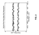
- FIG. 2 depicts a PMD measurement for the length of PM optical fiber referred to in FIG. 1 that is constructed using an embodiment of the present invention.
- the red line corresponds to the group delays for one measured PSP
- the blue line corresponds to the group delays of the other measured PSP.
- the group delays of a given PSP of FIG. 2 no longer incorrectly alternate between the high level (approximately 2 ps) and the low level (approximately -2 ps) as was the case in FIG. 1.
- a Jones matrix of a DUT represents the linear operation of the DUT on light.
- the Jones matrix describes the effect of the DUT on the phase, amplitude, and polarization of optical signals that are provided to the DUT.
- the software in memory 504 can include one or more separate programs, each of which comprises an ordered listing of executable instructions for implementing logical functions.
- the software in the memory 504 includes test system 100, which includes test signal generator module 520 and response analyzer module 530.
- the test signal generator module 520 provides control signals to a test signal generator that may be provided as a portion of the test system. Specifically, the test signal generator receives the control signals and provides optical signals of selected wavelengths to the DUT.
- Embodiments of the response analyzer module 530 will be described in detail later.
- test system 100 When test system 100 is implemented in software, it should be noted that the test system can be stored on any computer-readable medium for use by or in connection with any computer-related system or method.
- a computer-readable medium is an electronic, magnetic, optical, or other physical device or means that can contain or store a computer program for use by or in connection with a computer-related system or method.
- a computer-readable medium can be, for example but not limited to, an electronic, magnetic, optical, electromagnetic, infrared, or semiconductor system, apparatus, device, or propagation medium.
- the functionality of an embodiment of the test system (or method) 100 may be construed as beginning at block 610, where optical signals are provided to a DUT.
- the DUT responses to the optical signals are received.
- average values are computed that correspond to the phases and amplitudes associated with multiple wavelengths of optic signals.
- the average values are used to determine the fast and slow group delays associated with one of the optical signals.
- the differential group delay of the optical signal is determined using the fast and slow group delays.
- values corresponding to the phases and amplitudes of a particular element of a Jones matrix can be averaged over several wavelengths. The average values then can be used for that Jones matrix element.
- the values corresponding to multiple elements of a Jones matrix can be average values calculated over multiple wavelengths. Note, the wavelengths over which an average value is calculated for one element need not be the same wavelengths over which an average value is calculated for another element.
- FIG. 7 Functionality of another embodiment of the test system is depicted in FIG. 7.
- the functionality or method 100 may be construed as beginning at block 710, where optical signals are provided to a DUT.
- the DUT responses to the optical signals are received.
- the fast and slow group delays associated with at least some of the optical signals are determined.
- data corresponding to a subset of determined PSPs is received.
- another PSP e.g ., a measured eigenvector
- the measured PSP is compared to the subset of previously measured PSPs. Based on a relationship between the measured PSP and the subset of previously measured PSPs, the PSP is assigned to one of the first and second PSP, as depicted in block 770.
- Assignment of each of the measured eigenvectors then can be accomplished by determining which one of the eigenvectors more closely aligns with the previously determined first PSP and/or which of the eigenvectors more closely aligns with the previously determined second PSP.
- the polarized laser beam 819 and the fourth laser beam 820 are superimposed to produce interference resulting in the first superimposed laser beam 830.
- the first superimposed beam 830 is then coupled into a polarization beam splitter 832 that splits the first superimposed beam 830 into a seventh beam 834 and an eighth beam 836.
- Beam 834 is coupled into a first photodiode 838
- beam 836 is coupled into a second photodiode 840.
- the polarization beam splitter 832, first photodiode 838 and second photodiode 840 form a polarization diversity receiver.
- First photodiode 838 and second photodiode 840 transmit their outputs to an analog/digital-converter (ADC) 842 that communicates data to a response analyzer 530.
- ADC analog/digital-converter
- the polarization controller 826 imparts a defined polarization on the third laser beam 818, resulting in the polarized laser beam 819.
- the polarized laser beam 819 is coupled into the DUT 802.
- the polarized laser beam 819 is superimposed with the fourth laser beam 820, i.e., the reference arm of the Mach-Zehnder interferometer 844.
- the resulting first superimposed beam 830 is then coupled into the polarization beam splitter 832, which results in the seventh laser beam 834 and the eighth laser beam 836. Beams 834 and 836 are orthogonal, polarized components of beam 830.
- the remaining two elements of the Jones matrix of the DUT 802 are obtained by changing the polarization of the polarized laser beam 819 with the polarization controller 826 and performing the aforementioned steps in a second run, for example.
- the changed polarization of the resulting polarized laser beam (not shown) preferably is orthogonal to the polarization of the polarized laser beam 819 of the first run.
- optical characteristics of the DUT 802 such as PMD, DGD and PSPs can be determined. Note, additional information regarding interferometric determination of optical characteristics is presented in U. S. Patent Application Ser. No. 09/940,741, entitled, "Determination of Properties of an Optical Device," filed August 28, 2001, which claims priority to European Patent Application Ser. No. 01125089.3, filed on November 17, 2000, both of which are incorporated herein by reference.
- the PDL can be calculated using the eigenvalues associated with the two extreme polarizations, i.e., P + (associated with L + ) and P - (associated with L - ).
- P + associated with L +
- P - associated with L -
- This enables the measurement problem described above to be overcome by assigning each calculated eigenvalue to the proper P +, . before averaging occurs.
- the same measurement noise can lead to uncertainty in the determination of P + and P - .
- this means that errors can be made in distinguishing the two extreme polarizations, especially for cases in which the PDL is relatively small, e.g ., of the same order as the noise.
- An example of this effect was described previously with respect to FIG. 1 for PMD and will not be described in greater detail here. At least some embodiments of the invention are capable of alleviating this problem.
Landscapes
- Physics & Mathematics (AREA)
- Chemical & Material Sciences (AREA)
- Optics & Photonics (AREA)
- Analytical Chemistry (AREA)
- General Physics & Mathematics (AREA)
- Dispersion Chemistry (AREA)
- Testing Of Optical Devices Or Fibers (AREA)
- Investigating Or Analysing Materials By Optical Means (AREA)
Abstract
Description


Claims (10)
- A system (10) for determining optical characteristics of a device under test (DUT) (300), said system comprising:a test system (100) having a response analyzer (530) operative to receive data corresponding to responses of a DUT to optical signals of multiple wavelengths, compute fast and slow group delays corresponding to at least some of the optical signals, each of the fast and slow group delays being attributable to first and second principle states of polarization, and assign each of the fast and slow group delays to a correct one of the first and second principle states of polarization for at least some of the wavelengths.
- The system of claim 1, wherein an ability of the response analyzer to assign each of the fast and slow group delays to the correct one of the first and second principle states of polarization is not inhibited by the differential group delay of the DUT exhibiting an order of magnitude comparable to an order of magnitude of noise associated with the data received.
- The system of claim 1 or 2, wherein the response analyzer is operative to determine differential group delays of the DUT corresponding to at least some of the optical signals, each of the differential group delays being determined by subtracting a fast group delay from a corresponding slow group delay.
- The system of one of the preceding claims, further comprising:a tunable optical source (804) optically communicating with the DUT and operative to provide the optical signals to the DUT.
- The system of one of the preceding claims, further comprising:a polarization controller (826) optically communicating with the DUT and operative to impart selected polarizations to the optical signals provided to the DUT.
- The system of one of the preceding claims, wherein the response analyzer is operative to compute minimum and maximum insertion losses corresponding to at least some of the optical signals using the data received, the minimum and maximum insertion losses being attributable to first and second extreme states of polarization, and assign each of the minimum and maximum insertion losses to a correct one of the first and second extreme states of polarization for at least some of the wavelengths.
- The system of one of the preceding claims, wherein, in assigning each of the fast and slow group delays, the response analyzer is operative to receive data corresponding to a first subset of principle states of polarization of the DUT, receive data corresponding to another principle state of polarization of the DUT, compare the another principle state of polarization to the first subset of principle states of polarization, and assign the another principle state of polarization to one of the first and second principle states of polarization based on a relationship determined during the comparing.
- The system of one of the preceding claims, wherein, in computing the fast and slow group delays corresponding to the optical signals, the response analyzer is operative to compute an average value of at least some of the data associated with at least some of the optical signals, and use the average value to compute the fast and slow group delays corresponding to one of the optical signals.
- A method for determining optical characteristics of a device under test (DUT) (300), said method comprising:receiving data corresponding to responses of the DUT to optical signals of different wavelengths;computing minimum and maximum insertion losses corresponding to at least some of the optical signals using the data received, the minimum and maximum insertion losses being attributable to first and second extreme states of polarization; andassigning each of the minimum and maximum insertion losses to a correct one of the first and second extreme states of polarization for at least some of the wavelengths.
- The method of claim 9, wherein assigning each of the minimum and maximum insertion losses to the correct one of the first and second extreme states of polarization is not inhibited by a polarization dependent loss of the DUT exhibiting an order of magnitude comparable to an order of magnitude of noise associated with the receiving data step.
Applications Claiming Priority (2)
| Application Number | Priority Date | Filing Date | Title |
|---|---|---|---|
| US98284 | 2002-03-15 | ||
| US10/098,284 US6943891B2 (en) | 2002-03-15 | 2002-03-15 | Determining optical characteristics of optical devices under test |
Publications (2)
| Publication Number | Publication Date |
|---|---|
| EP1345021A2 true EP1345021A2 (en) | 2003-09-17 |
| EP1345021A3 EP1345021A3 (en) | 2004-03-24 |
Family
ID=27765430
Family Applications (1)
| Application Number | Title | Priority Date | Filing Date |
|---|---|---|---|
| EP02023225A Withdrawn EP1345021A3 (en) | 2002-03-15 | 2002-10-16 | Determining optical characteristics of optical devices under test |
Country Status (3)
| Country | Link |
|---|---|
| US (1) | US6943891B2 (en) |
| EP (1) | EP1345021A3 (en) |
| JP (1) | JP2003270096A (en) |
Families Citing this family (12)
| Publication number | Priority date | Publication date | Assignee | Title |
|---|---|---|---|---|
| US6882428B2 (en) * | 2001-08-28 | 2005-04-19 | Agilent Technologies, Inc. | Optical analyzer and method for reducing relative intensity noise in interferometric optical measurements using a continuously tunable laser |
| US6724468B2 (en) * | 2002-07-31 | 2004-04-20 | Agilent Technologies, Inc | Single sweep phase shift method and apparatus for measuring chromatic and polarization dependent dispersion |
| DE60203362T2 (en) * | 2002-08-22 | 2005-09-08 | Agilent Technologies, Inc. (n.d.Ges.d.Staates Delaware), Palo Alto | Averaging by polarization effects |
| JP2006214856A (en) * | 2005-02-03 | 2006-08-17 | Canon Inc | Measuring apparatus and method |
| JP4678236B2 (en) * | 2005-05-17 | 2011-04-27 | 横河電機株式会社 | Optical property measuring device |
| JP4753137B2 (en) * | 2005-11-29 | 2011-08-24 | 独立行政法人情報通信研究機構 | Calibration method and apparatus for light intensity measuring instrument |
| EP2568627A1 (en) * | 2011-08-30 | 2013-03-13 | Telefonaktiebolaget LM Ericsson (PUBL) | Optical signal monitoring method and apparatus |
| US10234501B2 (en) * | 2016-02-26 | 2019-03-19 | Tektronix, Inc. | Active noise suppression for optical voltage sensor |
| US9791346B1 (en) | 2016-04-20 | 2017-10-17 | Stmicroelectronics Sa | Semiconductor device and wafer with reference circuit and related methods |
| FR3054663B1 (en) * | 2016-07-28 | 2018-09-07 | Stmicroelectronics (Crolles 2) Sas | METHOD FOR CHARACTERIZING PHOTONIC DEVICES, AND ASSOCIATED DEVICE |
| FR3077888B1 (en) | 2018-02-13 | 2020-02-28 | Stmicroelectronics (Crolles 2) Sas | OPTOELECTRONIC CHIP AND METHOD FOR TESTING PHOTONIC CIRCUITS OF SUCH A CHIP |
| FR3077887B1 (en) | 2018-02-13 | 2021-07-23 | St Microelectronics Crolles 2 Sas | OPTOELECTRONIC CHIP AND METHOD FOR TESTING PHOTONIC CIRCUITS OF SUCH A CHIP |
Family Cites Families (4)
| Publication number | Priority date | Publication date | Assignee | Title |
|---|---|---|---|---|
| US4750833A (en) * | 1985-12-03 | 1988-06-14 | Princeton Applied Research Corp. | Fiber optic dispersion method and apparatus |
| FR2745082B1 (en) * | 1996-02-16 | 1998-04-30 | Univ Geneve | METHOD AND DEVICE FOR MEASURING THE POLARIZATION DISPERSION OF AN OPTICAL FIBER |
| JP3131144B2 (en) * | 1996-03-29 | 2001-01-31 | 株式会社アドバンテスト | Polarization mode dispersion measurement device |
| EP1113250B1 (en) | 2000-11-17 | 2003-02-05 | Agilent Technologies, Inc. (a Delaware corporation) | Method and apparatus for determining the polarisation mode dispersion of an optical device |
-
2002
- 2002-03-15 US US10/098,284 patent/US6943891B2/en not_active Expired - Fee Related
- 2002-10-16 EP EP02023225A patent/EP1345021A3/en not_active Withdrawn
-
2003
- 2003-03-10 JP JP2003063140A patent/JP2003270096A/en active Pending
Also Published As
| Publication number | Publication date |
|---|---|
| JP2003270096A (en) | 2003-09-25 |
| EP1345021A3 (en) | 2004-03-24 |
| US6943891B2 (en) | 2005-09-13 |
| US20030174337A1 (en) | 2003-09-18 |
Similar Documents
| Publication | Publication Date | Title |
|---|---|---|
| US6606158B2 (en) | Determination of a property of an optical device | |
| US20160123837A1 (en) | Devices and methods for characterization of distributed fiber bend and stress | |
| VanWiggeren et al. | Single-scan interferometric component analyzer | |
| US9829410B2 (en) | Distributed fiber bend and stress measurement for determining optical fiber reliability by multi-wavelength optical reflectometry | |
| US6882428B2 (en) | Optical analyzer and method for reducing relative intensity noise in interferometric optical measurements using a continuously tunable laser | |
| US6943891B2 (en) | Determining optical characteristics of optical devices under test | |
| US20040130724A1 (en) | Determining an optical property by using superimposed delayed signals | |
| US7009691B2 (en) | System and method for removing the relative phase uncertainty in device characterizations performed with a polarimeter | |
| US9041935B2 (en) | Measuring polarization crosstalk in optical birefringent materials and devices based on reduction of line broadening caused by birefringent dispersion | |
| US7920253B2 (en) | Polarization optical time domain reflectometer and method of determining PMD | |
| US7602499B2 (en) | Measuring polarization mode dispersion | |
| US5654793A (en) | Method and apparatus for high resolution measurement of very low levels of polarization mode dispersion (PMD) in single mode optical fibers and for calibration of PMD measuring instruments | |
| EP4027537B1 (en) | DEVICE AND METHOD FOR AN OPTICAL MULTI-MODE CHANNEL BANDWIDTH ANALYZER | |
| Williams | PMD measurement techniques and how to avoid the pitfalls | |
| EP1207377A2 (en) | Method and apparatus for measuring optical properties by means of the Jones matrix | |
| EP1191320B1 (en) | Measurement of polarization dependent characteristic of optical components | |
| JP2003172604A (en) | Phase noise compensation in interferometer systems | |
| Braunfelds et al. | Demonstration of polarization optical-time-domain reflectometer for monitoring of optical fiber lines | |
| AU6022896A (en) | Measurement of polarization mode dispersion | |
| US7349097B2 (en) | Interferometric determination of a transfer function of a device under test | |
| US6813028B2 (en) | Calibration methodology and system for optical network analyzer | |
| JP3998460B2 (en) | Method for determining characteristics of optical device and inspection device | |
| US6813027B2 (en) | Time difference synchronization for determination of a property of an optical device | |
| EP4498058A1 (en) | Method and apparatus of single-ended polarization mode dispersion measurement | |
| EP1329702B1 (en) | Polarization effect averaging |
Legal Events
| Date | Code | Title | Description |
|---|---|---|---|
| PUAI | Public reference made under article 153(3) epc to a published international application that has entered the european phase |
Free format text: ORIGINAL CODE: 0009012 |
|
| AK | Designated contracting states |
Kind code of ref document: A2 Designated state(s): AT BE BG CH CY CZ DE DK EE ES FI FR GB GR IE IT LI LU MC NL PT SE SK TR |
|
| AX | Request for extension of the european patent |
Extension state: AL LT LV MK RO SI |
|
| PUAL | Search report despatched |
Free format text: ORIGINAL CODE: 0009013 |
|
| AK | Designated contracting states |
Kind code of ref document: A3 Designated state(s): AT BE BG CH CY CZ DE DK EE ES FI FR GB GR IE IT LI LU MC NL PT SE SK TR |
|
| AX | Request for extension of the european patent |
Extension state: AL LT LV MK RO SI |
|
| RIC1 | Information provided on ipc code assigned before grant |
Ipc: 7G 01J 4/04 B Ipc: 7G 01M 11/00 A |
|
| 17P | Request for examination filed |
Effective date: 20040805 |
|
| AKX | Designation fees paid |
Designated state(s): DE FR GB |
|
| RAP1 | Party data changed (applicant data changed or rights of an application transferred) |
Owner name: AGILENT TECHNOLOGIES, INC. |
|
| GRAP | Despatch of communication of intention to grant a patent |
Free format text: ORIGINAL CODE: EPIDOSNIGR1 |
|
| STAA | Information on the status of an ep patent application or granted ep patent |
Free format text: STATUS: THE APPLICATION IS DEEMED TO BE WITHDRAWN |
|
| 18D | Application deemed to be withdrawn |
Effective date: 20080622 |