EP1341355A2 - Phase noise elimination for high-frequency communication - Google Patents
Phase noise elimination for high-frequency communication Download PDFInfo
- Publication number
- EP1341355A2 EP1341355A2 EP03004311A EP03004311A EP1341355A2 EP 1341355 A2 EP1341355 A2 EP 1341355A2 EP 03004311 A EP03004311 A EP 03004311A EP 03004311 A EP03004311 A EP 03004311A EP 1341355 A2 EP1341355 A2 EP 1341355A2
- Authority
- EP
- European Patent Office
- Prior art keywords
- phase
- frequency
- signal
- phase noise
- noise elimination
- Prior art date
- Legal status (The legal status is an assumption and is not a legal conclusion. Google has not performed a legal analysis and makes no representation as to the accuracy of the status listed.)
- Withdrawn
Links
Images




Classifications
-
- H—ELECTRICITY
- H04—ELECTRIC COMMUNICATION TECHNIQUE
- H04B—TRANSMISSION
- H04B1/00—Details of transmission systems, not covered by a single one of groups H04B3/00 - H04B13/00; Details of transmission systems not characterised by the medium used for transmission
- H04B1/06—Receivers
- H04B1/10—Means associated with receiver for limiting or suppressing noise or interference
- H04B1/1027—Means associated with receiver for limiting or suppressing noise or interference assessing signal quality or detecting noise/interference for the received signal
- H04B1/1036—Means associated with receiver for limiting or suppressing noise or interference assessing signal quality or detecting noise/interference for the received signal with automatic suppression of narrow band noise or interference, e.g. by using tuneable notch filters
-
- H—ELECTRICITY
- H04—ELECTRIC COMMUNICATION TECHNIQUE
- H04B—TRANSMISSION
- H04B1/00—Details of transmission systems, not covered by a single one of groups H04B3/00 - H04B13/00; Details of transmission systems not characterised by the medium used for transmission
- H04B1/06—Receivers
- H04B1/10—Means associated with receiver for limiting or suppressing noise or interference
- H04B1/12—Neutralising, balancing, or compensation arrangements
- H04B1/123—Neutralising, balancing, or compensation arrangements using adaptive balancing or compensation means
Definitions
- the present invention relates to a phase noise elimination circuit, a phase noise elimination apparatus and a high-frequency communication system which operate for phase modulated signals, in particular, QPSK (Quadri Phase Shift Keying) or other digital phase modulated signals to eliminate or reduce phase noise mixed from an oscillator.
- phase modulated signals in particular, QPSK (Quadri Phase Shift Keying) or other digital phase modulated signals to eliminate or reduce phase noise mixed from an oscillator.
- phase modulation system is a known technique, as described in detail in many books or literature such as "Digital Mobile Communications,” published by Tokyo Electrical Engineering College Publications.
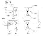
- Fig. 10 schematically shows a circuit of a communication system using the BPSK (Binary Phase Shift Keying) system that is the simplest among phase modulation systems.
- BPSK Binary Phase Shift Keying
- this communication system of Fig. 10 incorporates a reception system implemented by a synchronous detection system which is simple in circuit construction.
- upper-stage part represents a transmission system
- lower-stage part represents a receiver system
- reference numeral 117 denotes an input port for digital signals of the baseband
- 118 denotes an output port.
- 119 denotes a modulation part
- 120 denotes an up-convert part.
- 121 denotes a communication path, and this communication path 121 is implemented by a cable or the like for wire communications and by an antenna and a radio path for radio communications.
- numeral 122 denotes a down-convert part and 123 denotes a demodulation part.
- the modulation part 119 has an oscillator 124 and a mixer 141
- the up-convert part 120 has an oscillator 125 and a mixer 142
- the down-convert part 122 has an oscillator 126 and a mixer 143
- the demodulation part 123 has an oscillator 127, a mixer 144 and a low-pass filter 145.
- an output of the oscillator 124, which is relatively low in frequency, and a digital signal of the baseband are multiplied together by the mixer 141, by which a BPSK phase modulated signal is generated.
- a phase modulated signal which is taken over from the preceding stage, and an output of the oscillator 125, which is relatively high in frequency, are multiplied together by the mixer 142, by which the phase modulated signal is frequency-converted into a higher frequency band.
- the phase modulated signal that has passed through the communication path 121 is subjected in the down-convert part 122 to a conversion inverse to the conversion in the up-convert part 120.
- the signal derived from the up-convert part 120 is subject in the next demodulation part 123 to a conversion inverse to the conversion in the modulation part 119.
- This phase-modulation type communication system shown in Fig. 10 is a system that depends largely on the quality of the oscillators 124, 125, 126, 127.
- oscillators are used for not only frequency conversion of signals but also modulation and demodulation of signals.
- phase modulation system in which phase bears information, is a system sensitive particularly to phase noise of oscillators.
- phase noise of an oscillator refers to one of impure noise components PS0 contained in an output spectrum PS of the oscillator which should inherently be a pure sine wave PS1. More strictly, the noise component is further decomposed into amplitude component and phase component, and this phase component is referred to as phase noise.
- phase-modulation type communication system shown in Fig. 10, in all of the four oscillators 124 to 127, there is a fear that phase noise might be mixed into the phase modulated signal.
- phase noise is neighborhood noise
- phase noise PS0 has a spectrum continuously spreading on the axis of frequency.
- phase noise of immediate neighborhood of the sine-wave component inherent in the oscillator largely affects the communication quality, in particular.
- phase noise of a frequency band offset (shifted) from an oscillating frequency of 1 GHz by 10 kHz to 1 MHz largely affects the communication quality. Therefore, for expression of phase noise of the oscillator, logarithmic graphs are generally used.
- noise residing in extreme neighborhoods (10 kHz to 1 MHz offset) of a desired signal (1 GHz) as shown above it is impossible to adopt such a simple method as eliminating only noise, for example, by a band-pass filter. This is the essence of the difficulty in measures against phase noise.
- a typical one is to use a PLL (phase lock loop) circuit.
- PLL phase lock loop
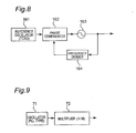
- a sampling-type PLL circuit is shown in Fig. 8. It is noted that this Fig. 8 is a diagram similar to Fig. 5.10(b) in the above-mentioned literature, "Monolithic Microwave Integrated Circuits (MMICs)."
- the phase of an oscillator 163 is compared to the phase of a high-stability reference oscillator 161 by a phase comparator 162. Through this phase comparison, the phase of the oscillator 163 is corrected and stabilized.
- the oscillator 163 is a VCO (Voltage Controlled Oscillator), and the reference oscillator 161 is a TCXO (Temperature Compensated Crystal Oscillator) or the like.
- phase noise reduction using this PLL circuit it has been becoming difficult to meet the demand of phase noise reduction that is going increasingly more strict year by year. This tendency is noticeable particularly in such extremely high frequency band as millimeter wave band. This is because, as described above, phase noise of an oscillator generally increases as the oscillating frequency becomes higher, which is a characteristic of the phase noise.
- a concrete example shown in Fig. 9 has an oscillator 171 containing a built-in PLL circuit and showing good phase-noise reduction performance in microwave band (frequency: 3.75 GHz), where a 16-fold multiplier 172 is connected to the oscillator 171, for use in millimeter wave band (frequency: 60 GHz).
- phase noise elimination other than the use of PLL circuits.
- An example is the technique in the field of optical communications, and a method disclosed in Japanese Patent Laid-Open Publication HEI 5-327415 is described with reference to Fig. 12.
- a signal issued from a signal source (light source) 130 is branched into two at a branch point 134, and one signal alone is passed through a delay line 131 and a phaser 132. This one signal is combined with the other signal in a mixer 133.
- the noise elimination technique explained in this Fig. 12 is a technique in the field of optical communications, and cannot be implemented in electrical circuits as it is. This is because in the prior art technique of Fig. 12, optical fibers extending as long as several hundreds meters to several kilometers are used as the delay line 131. Although optical fibers small in loss and thin in diameter could implement such a constitution, yet it can be said impractical to connect together coaxial cables for electric signals large in loss and thick in diameter over lengths of several hundreds meters to several kilometers from the viewpoints of loss and size.
- an object of the present invention is to provide a phase noise elimination circuit, a phase noise elimination apparatus and a high-frequency communication system which can be implemented by small-size, low-cost, easy-to-mass-produce electrical circuits.
- phase noise elimination circuit comprising:
- the inputted high-frequency signal is branched into two high-frequency signals by the branching part, and one high-frequency signal out of the two branched high-frequency signals is passed through the surface-acoustic-wave delay line or bulk-acoustic-wave delay line.
- the high-frequency signal can be delayed by a specified time as compared to the other high-frequency signal.
- the one high-frequency signal delayed by a specified time as compared to the other high-frequency signal and the other high-frequency signal are adjusted by the phase amplitude adjustment part so as to become generally equal in amplitude and phase of their respective non-noise signal components to each other.
- the noise signal component of the one high-frequency signal is delayed by the specified time due to the delay line as compared to the noise signal component of the other high-frequency signal.
- the two high-frequency signals which have been adjusted so as to be generally equal to each other in amplitude and phase of their non-noise signal components and which have been shifted from each other in amplitude and phase of their noise signal components by the specified time as shown above, are combined together by the combining part.
- the in-phase two non-noise signals out of the two high-frequency signals intensify each other, while the phase-shifted two noise signals out of the two high-frequency signals cancel each other.
- one high-frequency signal is passed through the surface-acoustic-wave delay line or bulk-acoustic-wave delay line, so that its non-noise signal component and noise signal component are shifted in phase from each other.
- the other high-frequency signal is not passed through the surface-acoustic-wave delay line or the bulk-acoustic-wave delay line, so that the noise signal component of the other high-frequency signal is shifted in phase from the noise signal component of the one high-frequency signal.
- a delay line has been implemented by an electrical circuit which is small in scale, low in cost and easy to mass produce by using as an acoustic wave delay line, i.e., a SAW (surface acoustic wave) delay line or a BAW (bulk acoustic wave) delay line.
- a SAW surface acoustic wave
- BAW bulk acoustic wave
- the acoustic wave delay line is a known technique disclosed in much literature such as "A Handbook for Acoustic Wave Device Technique,” edited by No. 150 Committee for Acoustic Wave Device Technique, the Japan Society for the Promotion of Science (Ohmsha), and a device for once converting an electric signal into an ultrasonic wave signal, subjecting the signal to a propagation delay, and then returning the signal again to the electric signal.
- the propagation velocity of an electric signal on an electronic circuit board is generally about several tens percent of the velocity of light (3 ⁇ 10 8 m/sec.).
- the propagation velocity of ultrasonic waves on a piezoelectric board is generally on the order of several hundreds to several thousands (m/sec.), slower than that of electric signals by an order of 10 -5 . That is, given an equal device size, devices of ultrasonic propagation can achieve delay times larger than those of devices of electric signal propagation by an order of 10 5 . As a result of this, the size of delay lines implemented by electrical circuits can be reduced.
- acoustic-wave type delay lines generally involve smaller amounts of occurrence of insertion loss, than coaxial-line type delay lines, to achieve the same delay time. Therefore, the loss of delay lines implemented by electrical circuits can be reduced.
- acoustic wave delay lines, in particular, SAW (surface acoustic wave) delay line are devices which are mass produced by manufacturing processes similar to those of semiconductor integrated circuits (ICs), thus good in mass productivity.
- phase noise elimination apparatus having a plurality of the above phase noise elimination circuits, wherein the plurality of phase noise elimination circuits are connected in a plurality of stages.
- phase noise elimination circuit since the phase noise elimination circuit is connected in a plurality of stages, phase noise can be reduced to an extent beyond the limit of the prior art by multiplier effects of this plurality of stages of phase noise elimination circuits.
- the phase noise elimination circuits of the individual stages have different values of delay time of the surface-acoustic-wave delay line or bulk-acoustic-wave delay line.
- phase noise elimination apparatus of this embodiment since the phase noise elimination circuits of the individual stages have different values of delay time of the surface-acoustic-wave delay line or bulk-acoustic-wave delay line, frequencies of phase noise to be eliminated in the individual stages are made different from one another, so that the phase noise elimination effect can be obtained over a wider range of offset frequency.
- a high-frequency communication system equipped with a phase modulator or a phase demodulator, wherein the above phase noise elimination circuit is connected between a reference oscillator of the phase modulator or the phase demodulator and a modulation-and-demodulation use mixer.
- phase noise elimination circuit (or the above-described phase noise elimination apparatus) is connected between a reference oscillator of the phase modulator or the phase demodulator and a modulation-and-demodulation use mixer. Therefore, by this phase noise elimination circuit or apparatus, phase noise can be eliminated from high-frequency signals outputted by the reference oscillator of the phase modulator or phase demodulator.
- phase noise elimination circuit is connected between a local oscillator and a mixer.
- phase noise elimination circuit (or the above-described phase noise elimination apparatus) is connected between a local oscillator and a mixer. Therefore, by this phase noise elimination circuit or apparatus, phase noise can be eliminated from high-frequency signals outputted by the local oscillator.
- Fig. 1 shows the basic construction of a first embodiment of the phase noise elimination circuit according to the present invention.
- an electric power distribution part 3 is connected to an input port 1, while a phase amplitude adjustment part 7 and an acoustic wave delay part 5 are connected to the power distribution part 3.
- the acoustic wave delay part 5 is connected to a phase amplitude adjustment part 6, while the phase amplitude adjustment part 6 and the phase amplitude adjustment part 7 are connected to an electric power combining part 4.
- the power combining part 4 is connected to an output port 2.
- the power distribution part 3 and the power combining part 4 can easily be implemented by using, for example, a Wilkinson-type power divider or the like which is a known technique.
- the acoustic wave delay part 5 is provided by an acoustic wave delay line.
- This acoustic wave delay line may be a SAW (Surface Acoustic Wave) delay line or a BAW (Bulk Acoustic Wave) delay line.
- Fig. 4 schematically shows an example of the SAW delay line.
- an input-side comb-type electrode pair 9 and an output-side comb-type electrode pair 10 are disposed on a piezoelectric substrate 8 formed by cutting a piezoelectric crystal material.
- These input-side comb-type electrode pair 9 and output-side comb-type electrode pair 10 are spaced from each other by a specified distance, where a region of the piezoelectric substrate 8 between the input-side comb-type electrode pair 9 and the output-side comb-type electrode pair 10 serves as a propagation path 11.
- the comb-type electrode pairs 9 and 10 are implemented by pairs of combined comb-type electrodes 9a, 9b and 10a, 10b, respectively.
- the comb-type electrode pairs 9 and 10 are obtained each through a step of forming a film of Al or other metal on the piezoelectric substrate 8 by common semiconductor manufacturing process such as evaporation, and a step of patterning by photolithography process.
- the surface acoustic wave that has reached this output-side comb-type electrode pair 10 is converted into an electric signal, and taken out as a voltage difference between the terminals 47, 48 connected to the electrodes 10a, 10b of the output-side comb-type electrode pair 10.
- phase amplitude adjustment parts 6, 7 are implemented each by a circuit that performs fine adjustment of phase and amplitude of an electric signal. Fine adjustment of the amplitude of an electric signal can easily be fulfilled by using an amplifier or attenuator of known techniques, and so can fine adjustment of its phase be done also by using a delay line or phase shifter of known techniques. It is noted that these phase amplitude adjustment parts 6, 7 do not necessarily need to be provided in a total number of two as shown in Fig. 1. It is also allowable to provide only either one of the phase amplitude adjustment part 6 or 7 only if two electric signals to be combined together in the power combining part 4 can be made equal in phase and amplitude to each other. It is yet also allowable, for example, to distribute the function between adjustment parts 6 and 7 so that the adjustment part 6 has only the amplitude adjustment function while the adjustment part 7 has only the phase adjustment function.
- a high-frequency signal inputted to the power distribution part 3 from the input port 1 is branched into two high-frequency signals.
- One high-frequency signal is inputted to the acoustic wave delay part 5, while the other high-frequency signal is inputted to the phase amplitude adjustment part 7.
- the high-frequency signal inputted to the acoustic wave delay part 5 is delayed by a delay time T, inputted to the phase amplitude adjustment part 6, and thereafter inputted to the power combining part 4.
- two high-frequency signals derived from the phase amplitude adjustment parts 6 and 7 are inputted and combined together, and then outputted to the output port 2.
- this frequency offset df is several Hz to several MHz, whereas the delay time T is on the order of ⁇ seconds.
- the delay time T is 50 ⁇ s and the frequency offset df is 10 kHz
- the two high-frequency signals combined together in the power combining part 4 are preparatorily adjusted by the phase amplitude adjustment parts 6 and 7 so that their signal components of the frequency fc, which is the carrier signal, become equal in phase and amplitude to each other.
- the noise signal components of the frequency fn come to have a phase shift of 180° between a noise signal component S1n of the frequency fn contained in a high-frequency signal S1 derived from the phase amplitude adjustment part 7 and a noise signal component S2n of the frequency fn contained in a high-frequency signal S2 derived from the phase amplitude adjustment part 6.
- T is the delay time and n is an arbitrary natural number including zero.
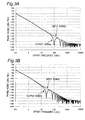
- Figs. 3A and 3B show characteristics obtained by verifying phase noise reduction effects through calculations performed by a commercially available nonlinear circuit simulator (Serenade 8.5 made by Ansoft) on the phase noise elimination circuit of the first embodiment shown in Fig. 1.
- the carrier frequency fc was set to 850 MHz and practical numerical values were given as phase noise values beforehand for modeling.
- the delay time T of the acoustic wave delay part 5 was set to 5 ⁇ s in Fig. 3A, while the delay time T of the acoustic wave delay part 5 was set to 20 ⁇ s in Fig. 3B. It can be understood that phase noise that had been contained in an input signal Sin from the input port 1 was canceled in an output signal Sout from the output port 2 in specific offset frequencies, respectively.
- Fig. 2 shows characteristics obtained by actually verifying phase noise elimination effects through a measuring experiment on the phase noise elimination circuit of the first embodiment shown in Fig. 1.
- the acoustic wave delay part 5 was implemented by a SAW delay line having a delay time T of 2.5 ⁇ s, a center frequency of 850 MHz, a bandwidth of 200 MHz and an insertion loss of about 25 dB.
- a SAW delay line having a relatively short delay time T of 2.5 ⁇ s was used.
- the frequency of the carrier signal was set to 922 MHz, and a semi-microwave band signal generator was used as a signal source for inputting a high-frequency signal to the input port 1.
- the phase amplitude adjustment part 6 was made up of an amplifier having a gain of about 25 dB, a coaxial attenuator, coaxial phaser parts, and a coaxial cable.
- the phase amplitude adjustment part 7 was made up of a coaxial attenuator, a coaxial phaser part, and a coaxial cable.
- the power distribution part 3 and the power combining part 4 were implemented by coaxial power dividers.
- a commercially available phase noise analyzer (NTS-1000B made by RDL) was used.
- the center frequency on which the SAW delay line operates is limited to that of about 1 GHz at most, and SAW delay lines that operate on center frequencies of millimeter wave band have not yet be realized.
- the phase noise elimination circuit of the first embodiment of the invention is applied to a high-frequency communication system that operates with carrier signals of superhigh frequency band such as millimeter wave band
- a system equipped with an oscillator 71 having an oscillating frequency of 1 GHz or lower and a frequency multiplier 72 is adopted, where a phase noise elimination circuit 73 of the above-described embodiment is connected between the oscillator 71 and the frequency multiplier 72, as shown in Fig. 7.
- an output signal of 1 GHz or lower outputted by the oscillator 71 is subjected to noise elimination by the phase noise elimination circuit 73, and the signal from which noise has been eliminated is multiplied to a frequency of the millimeter wave band by the frequency multiplier 72.
- the center frequency of the SAW delay line does not necessarily need to be a high frequency over 1 GHz.
- the bandwidth of the SAW delay line does not matter in performing the phase noise elimination for a sine-wave output of the oscillator 71.
- the insertion loss of the SAW delay line is quite large in general, being about 20 to 40 dB in many cases. Whereas the smaller insertion loss of the SAW delay line is preferable, insertion losses of particularly 25 dB or lower can be compensated only by adding one stage of amplifier in many cases, thus advantageous for downsizing of the whole high-frequency communication system.
- the delay time T In the state-of-the-art digital communications, it is often the case that phase noise in the vicinity of a frequency offset by 10 Hz to 100 kHz is of importance. From the foregoing calculational equation (4), it can be understood that a delay time T of 5 ⁇ s to 50 ms is needed to eliminate the phase noise of such offset frequencies.
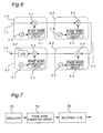
- Fig. 5 shows an example of a phase noise elimination apparatus which is a second embodiment of the invention.
- the phase noise elimination circuit of the foregoing embodiment is connected in multiple stages, allowing an even greater phase noise elimination effect to be realized.
- phase noise elimination circuits 13, 14 of the foregoing first embodiment are connected together in multiple stages in order to obtain a phase noise elimination effect far beyond the limit of the prior art technique.
- phase noise elimination circuit 13 included in this second embodiment can be used in cascade connection (series connection) without obstructing the operation of the oscillator 12 formed of a PLL circuit at all. Since the first embodiment, which is a phase noise elimination circuit according to the present invention, is a transmission type circuit, it is possible to use the phase noise elimination circuit 14 in cascade connection to the phase noise elimination circuit 13. Also, although not shown, similar phase noise elimination circuits may also be used in further cascade connection.
- a PLL circuit is a 1-port circuit integrated with an oscillator, and could not be applied into multiple stages as it is.
- the phase noise elimination circuit of the first embodiment according to the present invention is a 2-port transmission-type circuit, thus allowing itself to be applied to multiple stages as in this second embodiment.
- Fig. 6 shows a phase modulated signal communication system which is a third embodiment of the invention.
- This communication system has a modulation part 19 and an up-convert part 20 which are cascade-connected to an input port 17 for a baseband digital signal. These modulation part 19 and up-convert part 20 constitute a transmitting system.
- the up-convert part 20 of this transmitting system leads to a down-convert part 22 of a receiver system via a communication path 21.
- This down-convert part 22 is connected to a demodulation part 23, and this demodulation part 23 leads to an output port 18.
- the modulation part 19 is composed of a modulation-use oscillator 24, a mixer 41, and a phase noise elimination circuit 51 connected between the modulation-use oscillator 24 and the mixer 41.
- the up-convert part 20 is composed of a frequency-conversion use local oscillator 25, a mixer 42, and a phase noise elimination circuit 52 connected between the oscillator 25 and the mixer 42.
- the down-convert part 22 is composed of a frequency-conversion use local oscillator 26, a mixer 43, and a phase noise elimination circuit 53 connected between the oscillator 26 and the mixer 43.
- the demodulation part 23 is composed of a demodulation-use oscillator 27, a mixer 44, a low-pass filter 45, and a phase noise elimination circuit 54 connected between the oscillator 27 and the mixer 44.
- the phase noise elimination circuits 51, 52, 53, 54 are implemented each by the phase noise elimination circuit of the foregoing first embodiment.
- the oscillators 24 to 27, the mixers 41 to 44 and the low-pass filter 45 are the same as the oscillators 124 to 127, mixers 141 to 144, and the low-pass filter 145, respectively, in the prior art of Fig. 10, and so their description is omitted.
- phase noise elimination circuits 51, 52, 53, 54 are connected for the four oscillators 24 to 27 (i.e., all of the modulation-use oscillator 24, the demodulation-use oscillator 27, the frequency-conversion use local oscillators 25 and 26), respectively.
- These phase noise elimination circuits 51, 52, 53, 54 are capable of performing the phase noise elimination in an additional mode regardless of the internal structure of the oscillators 24 to 27 as described above.
- phase noise elimination circuits 52 and 53 to those local oscillators 25 and 26 allows a large extent of phase noise reduction to be achieved.
- phase noise to be mixed into the system as a whole can be reduced to a large extent, so that the communication quality can be improved.
- phase noise elimination circuits 51 to 54 that are small in scale and easy to mass produce, phase noise of the oscillators 24 to 27 can be reduced.
- the phase noise elimination circuits 51 to 54 that are small in scale and easy to mass produce, phase noise of the oscillators 24 to 27 can be reduced.
- phase noise reduction circuits 51 to 54 do not obstruct the operation of other phase noise reduction circuits, such as PLL circuits, of the prior art, but lend themselves to use in series connection in pluralities to those other phase noise reduction circuits. Thus, by their multiplier effects, the phase noise can be reduced to an extent beyond the limitations of the prior art.
Landscapes
- Engineering & Computer Science (AREA)
- Computer Networks & Wireless Communication (AREA)
- Signal Processing (AREA)
- Noise Elimination (AREA)
Abstract
Description
the above phase noise elimination circuit is connected between a reference oscillator of the phase modulator or the phase demodulator and a modulation-and-demodulation use mixer.
the phase noise elimination circuit is connected between a local oscillator and a mixer.
Claims (7)
- A phase noise elimination circuit comprising:a branching part (3) for branching an inputted high-frequency signal into two high-frequency signals;a surface-acoustic-wave delay line (5) or bulk-acoustic-wave delay line to which one high-frequency signal out of the two branched high-frequency signals is to be inputted;a phase amplitude adjustment part (6, 7) for adjusting amplitude and phase of non-noise signal components contained in a high-frequency signal that has passed through the surface-acoustic-wave delay line (5) or bulk-acoustic-wave delay line and amplitude and phase of non-noise signal components contained in the other high-frequency signal out of the two high-frequency signals so as to make their amplitudes and phases generally coincident with each other; anda combining part (4) for combining together two high-frequency signals outputted by the phase amplitude adjustment parts (6, 7) and containing non-noise signal components adjusted so that their amplitude and phase become generally equal to each other.
- A phase noise elimination apparatus having a plurality of phase noise elimination circuits as defined in Claim 1, wherein the plurality of phase noise elimination circuits are connected in a plurality of stages.
- The phase noise elimination apparatus according to Claim 2, wherein
the phase noise elimination circuits of the individual stages have different values of delay time (T) of the surface-acoustic-wave delay line (5) or bulk-acoustic-wave delay line. - A high-frequency communication system equipped with a phase modulator or a phase demodulator, wherein
the phase noise elimination circuit (51, 54) as defined in Claim 1 is connected between a reference oscillator (24, 27) of the phase modulator or the phase demodulator (19, 23) and a modulation-and-demodulation use mixer (41, 44). - A high-frequency communication system equipped with a phase modulator or a phase demodulator, wherein
the phase noise elimination apparatus as defined in Claim 2 or 3 is connected between a reference oscillator (24, 27) of the phase modulator or the phase demodulator (19, 23) and a modulation-and-demodulation use mixer (41, 44). - A high-frequency communication system for mixing phase modulated signal with a local signal to fulfill frequency conversion of the phase modulated signal, wherein
the phase noise elimination circuit as defined in Claim 1 is connected between a local oscillator and a mixer. - A high-frequency communication system for mixing phase modulated signal with a local signal to fulfill frequency conversion of the phase modulated signal, wherein
the phase noise elimination apparatus as defined in Claim 2 or 3 is connected between a local oscillator and a mixer.
Applications Claiming Priority (2)
| Application Number | Priority Date | Filing Date | Title |
|---|---|---|---|
| JP2002055917 | 2002-03-01 | ||
| JP2002055917A JP2003258657A (en) | 2002-03-01 | 2002-03-01 | Phase noise removing circuit, phase noise removing apparatus, and high frequency communication system |
Publications (2)
| Publication Number | Publication Date |
|---|---|
| EP1341355A2 true EP1341355A2 (en) | 2003-09-03 |
| EP1341355A3 EP1341355A3 (en) | 2006-11-08 |
Family
ID=27678590
Family Applications (1)
| Application Number | Title | Priority Date | Filing Date |
|---|---|---|---|
| EP03004311A Withdrawn EP1341355A3 (en) | 2002-03-01 | 2003-02-27 | Phase noise elimination for high-frequency communication |
Country Status (2)
| Country | Link |
|---|---|
| EP (1) | EP1341355A3 (en) |
| JP (1) | JP2003258657A (en) |
Cited By (4)
| Publication number | Priority date | Publication date | Assignee | Title |
|---|---|---|---|---|
| FR2869483A1 (en) * | 2004-04-21 | 2005-10-28 | Sagem | SPREAD SPECTRUM SIGNAL BROKER REJECTOR METHOD AND DEVICE |
| CN102130879A (en) * | 2011-03-10 | 2011-07-20 | 上海交通大学 | Phase Noise Elimination Method in OFDM System |
| US11375462B2 (en) | 2017-03-24 | 2022-06-28 | Samsung Electronics Co., Ltd. | Method and apparatus for phase tracking reference signal in a wireless communication system |
| US11552754B2 (en) | 2017-05-05 | 2023-01-10 | Samsung Electronics Co., Ltd. | Method and apparatus for phase tracking reference signal in a wireless communication system |
Families Citing this family (3)
| Publication number | Priority date | Publication date | Assignee | Title |
|---|---|---|---|---|
| KR101340757B1 (en) | 2007-03-09 | 2014-01-02 | 삼성전자주식회사 | Method and apparatus for removing noise using phase difference and spectrum energy |
| CN101453228B (en) * | 2007-12-04 | 2013-04-17 | 松下电器产业株式会社 | Common station address interference elimination system and method |
| JP7636002B2 (en) | 2022-08-03 | 2025-02-26 | デバイス株式会社 | Noise Canceller Device |
Family Cites Families (4)
| Publication number | Priority date | Publication date | Assignee | Title |
|---|---|---|---|---|
| US4968908A (en) * | 1989-03-06 | 1990-11-06 | The United States Of America As Represented By The Secretary Of Commerce | Method and apparatus for wide band phase modulation |
| US5077546A (en) * | 1990-11-07 | 1991-12-31 | General Electric Company | Low phase noise frequency multiplier |
| JPH05327415A (en) * | 1991-07-24 | 1993-12-10 | Nakano Syst:Yugen | Phase noise canceller |
| US5661439A (en) * | 1996-07-11 | 1997-08-26 | Northrop Grumman Corporation | Method and apparatus for cancelling phase noise |
-
2002
- 2002-03-01 JP JP2002055917A patent/JP2003258657A/en active Pending
-
2003
- 2003-02-27 EP EP03004311A patent/EP1341355A3/en not_active Withdrawn
Cited By (6)
| Publication number | Priority date | Publication date | Assignee | Title |
|---|---|---|---|---|
| FR2869483A1 (en) * | 2004-04-21 | 2005-10-28 | Sagem | SPREAD SPECTRUM SIGNAL BROKER REJECTOR METHOD AND DEVICE |
| EP1596503A1 (en) * | 2004-04-21 | 2005-11-16 | Sagem S.A. | Device and method for rejecting interference in a spread spectrum signal |
| CN102130879A (en) * | 2011-03-10 | 2011-07-20 | 上海交通大学 | Phase Noise Elimination Method in OFDM System |
| CN102130879B (en) * | 2011-03-10 | 2013-08-21 | 上海交通大学 | Phase noise elimination method in orthogonal frequency division multiplexing system |
| US11375462B2 (en) | 2017-03-24 | 2022-06-28 | Samsung Electronics Co., Ltd. | Method and apparatus for phase tracking reference signal in a wireless communication system |
| US11552754B2 (en) | 2017-05-05 | 2023-01-10 | Samsung Electronics Co., Ltd. | Method and apparatus for phase tracking reference signal in a wireless communication system |
Also Published As
| Publication number | Publication date |
|---|---|
| JP2003258657A (en) | 2003-09-12 |
| EP1341355A3 (en) | 2006-11-08 |
Similar Documents
| Publication | Publication Date | Title |
|---|---|---|
| Qin et al. | Broadband parametric circulator with balanced monolithic integrated distributedly modulated capacitors (DMC) | |
| US7139329B2 (en) | Receiver in a radio communication system | |
| US20050090274A1 (en) | Communication system | |
| US7127227B2 (en) | Digital down-converter | |
| CN111987995B (en) | Comb signal source based on frequency mixing modulation feedback loop | |
| US9379798B2 (en) | Modulation circuit for a radio device and a method thereof | |
| US5373256A (en) | PLL frequency synthesizer having a main loop and a secondary loop | |
| EP1341355A2 (en) | Phase noise elimination for high-frequency communication | |
| EP2237423A1 (en) | Frequency synthesizer | |
| CN110868210A (en) | Frequency synthesis method and frequency synthesis device | |
| Hikita et al. | A wideband SAW resonator and its application to a VCO for mobile radio transceivers | |
| CN116488734A (en) | Tunable millimeter wave frequency generating device | |
| Urabe et al. | New SAW oscillators for land mobile telephone radio unit | |
| Bhavsar et al. | High Frequency Integrated Microwave Circuit Board Designed for the X-band Signal Generation | |
| Dengler et al. | A compact 600 GHz electronically tunable vector measurement system for submillimeter wave imaging | |
| Ilchenko et al. | Development of the transmitting and receiving channels for terahertz band relay systems | |
| Grant et al. | Surface wave device applications in microwave communication systems | |
| EP1357667B1 (en) | Frequency synthesizer and transceiver including same | |
| RU2830675C1 (en) | Synthesizer with low level of phase noise | |
| Lin et al. | A low phase-noise voltage-controlled SAW oscillator with surface transverse wave resonator for SONET application | |
| Fleischmann et al. | A 2.5 GHz low noise phase locked surface transverse wave VCO | |
| CN224124126U (en) | A frequency synthesizer receiver module with full-function output | |
| US20010016017A1 (en) | Quadrature modulator | |
| CN111510140B (en) | Clock local oscillator assembly | |
| CN223139834U (en) | Multi-channel radio frequency receiver applying comb spectrum calibration |
Legal Events
| Date | Code | Title | Description |
|---|---|---|---|
| PUAI | Public reference made under article 153(3) epc to a published international application that has entered the european phase |
Free format text: ORIGINAL CODE: 0009012 |
|
| AK | Designated contracting states |
Kind code of ref document: A2 Designated state(s): AT BE BG CH CY CZ DE DK EE ES FI FR GB GR HU IE IT LI LU MC NL PT SE SI SK TR |
|
| AX | Request for extension of the european patent |
Extension state: AL LT LV MK RO |
|
| PUAL | Search report despatched |
Free format text: ORIGINAL CODE: 0009013 |
|
| AK | Designated contracting states |
Kind code of ref document: A3 Designated state(s): AT BE BG CH CY CZ DE DK EE ES FI FR GB GR HU IE IT LI LU MC NL PT SE SI SK TR |
|
| AX | Request for extension of the european patent |
Extension state: AL LT LV MK RO |
|
| RIC1 | Information provided on ipc code assigned before grant |
Ipc: H03B 5/04 20060101ALI20060929BHEP Ipc: H04B 15/06 20060101ALI20060929BHEP Ipc: H04B 1/10 20060101AFI20060929BHEP |
|
| 17P | Request for examination filed |
Effective date: 20070416 |
|
| AKX | Designation fees paid |
Designated state(s): DE FR |
|
| 17Q | First examination report despatched |
Effective date: 20070621 |
|
| STAA | Information on the status of an ep patent application or granted ep patent |
Free format text: STATUS: THE APPLICATION IS DEEMED TO BE WITHDRAWN |
|
| 18D | Application deemed to be withdrawn |
Effective date: 20071103 |