Technical Field
The present invention relates to a method and an apparatus for
time equalization, and in particular to a method and an apparatus for
time equalization employed in modems or the like used at the time of
a superfast data transmission with metallic wires.
Background Art
Generally, modems have been used for transmitting data with
telephone lines, leased lines, private metallic wires, or the like, while
in recent years, enhanced speed has been in demand for the
processing of modem.
As a technical field where such modems are used, e.g. a
power-line carrier communication can be mentioned. This power-line
carrier communication includes an extremely large amount of random
noises (white noises) from household electrical appliances such as an
inverter, which blocks practical utilization of a high-speed data
communication.
As recent countermeasures for such noises, a DMT (Discrete
MultiTone) system and an OFDM (Orthogonal Frequency Division
Multiplexing) system have been proposed. These DMT system and
OFDM system adopt a multicarrier (multichannel) modulation system,
that is a technology which avoids a signal from passing through a
carrier band rich in noises. However, the multicarrier causes a group
delay, as shown in Fig.12(2), in a transmission line on route, even if
signals of channels are simultaneously transmitted from a
transmission side as shown in Fig.12(1). As a result, arrival times of
the channels on a time axis are different from each other on a
reception side, as shown in Fig.12(3). For this reason, an inter-channel
interference on a time axis arises on the reception side.
Namely, since low-speed square waves are transmitted in the
DMT system or the OFDM system as shown in Fig.13, a normal
transmission signal (tone) can be obtained, as shown in Fig.13(2), in a
stable part of the square wave. However, in a variable part of the
square wave, unnecessary bands of each channel have a waveform
attenuating at a function of sinx/x as shown in Figs.13(1) and 13(3).
Thus, in a line characteristic where the group delay arises, the
signals of the channels interfere with each other on a time axis, and
the inter-channel interference is avoided only in a flat part of the line
characteristic.
On one hand, if a time corresponding to the interference part (i.e.
time corresponding to a variable time of the square wave) is masked
as a guard time GT as shown in Fig.13, it becomes possible to avoid
the inter-channel interference. However, data transmission is disabled
for this guard time GT, which makes a high-speed transmission
difficult.
Accordingly, equalization between channels on a time axis is
necessary in order to solve such a problem of a line group delay.
On the other hand, even in the same apparatus, the static
characteristic greatly differs depending on ON/OFF state of power. In
household electrical appliances such as a television using a switching
power, two transfer functions A (or C) and B (or D) are alternately
switched over every 120 Hz (in case a used frequency is 60 Hz)
depending on whether the voltage is equal to or less than or more than
a fixed value as shown in Fig.14(1). Namely, the transfer functions are
switched over 240 times per second.
Thus, if the transfer function varies, a frequency characteristic
(amplitude/phase) is divided into a solid line indicating the transfer
functions A and C and a dotted line indicating the transfer functions B
and D, as shown in Fig.14(2), both being greatly different from each
other. Such a variation of the phase characteristic also includes the
variation on a time axis.
Accordingly, since a high-speed followup performance is required
for the transmission line in a modem or the like used for the
power-line carrier communication, not only the high-speed
equalization on a time axis as mentioned above, but also equalization
on a frequency axis is required. If the equalization on a time axis is
performed, it will contribute to the equalization on the frequency axis.
Fig.15 shows a prior art for realizing the above-mentioned
equalization on a time axis and a frequency axis. This prior art is
composed of a time equalizer 1, a guard time remover 2, a DMT
distributor 3 by an FFT (Fast Fourier Transform) calculation, a
frequency equalizer (FEQ) 4, a determining portion (DEC) 5, and a
code inverter 6, all being connected in series.
In this arrangement, the time equalizer 1 performs the
equalization on a time axis to the received signal, and then the guard
time remover 2 removes the guard time added on the transmission
side. Furthermore, the DMT distributor 3 performs the FFT. Then, the
frequency equalizer 4 performs the equalizations of the carrier
amplitude and the carrier phase, and the determining portion 5
determines the code. Then, the code inverter 6 performs the code
conversion such as Natural (N)/Gray (G) code conversion, a parallel
(P)/serial (S) conversion, and descramble (DSCR) to obtain the
received data RD.
In such a prior art, a special training signal is required in order
to perform pull-in on a time axis at the time equalizer 1. This training
signal requires a long time, and complicated processing for this
training.
Namely, since a high-speed followup performance is required for
the line characteristic which varies every 120 Hz, as mentioned above,
at a multi point of 1:n, it is not possible to provide a long training time
at each point, so that simple processing is required.
It is accordingly an object of the present invention to provide a
method and an apparatus for performing time equalization to a line
group delay of a received signal with a short training time.
Disclosure of Invention
In order to achieve the above-mentioned object, a time
equalization method according to the present invention comprises: a
first step of extracting timing phase information from a power
spectrum of a received signal whose amplitude is modulated per frame
or sub-frame; and a second step of performing timing phase
synchronization of the received signal with this timing phase
information.
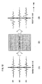
Namely, frequency signals simultaneously transmitted by
different channels are respectively received at different times, as
shown in Fig.1(1), due to a line group delay characteristic.
In the present invention, by performing a timing phase control
shown in Fig.1(2), a time equalization is performed to signal
waveforms having arrived at different times respectively as shown in
Fig.1(1) in accordance with the line group delay characteristic, thereby
aligning signal arrival times as shown in Fig.1(3).
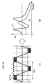
Focusing on a waveform of a single channel, it is found, as shown
in Fig.2(1), that an original reception point deviates from a sample
point before performing the equalization of the timing phase by the
present invention. In this state, the inter-channel interference arises.
After performing the equalization of the timing phase, as shown
in Fig.2(2), in the present invention, the reception point coincides with
the sample point at all the channels, so that the inter-channel
interference is eliminated, and the problems shown in Figs.12 and 13
are solved, thereby enabling the high-speed transmission.
When an amplitude modulation is performed per frame, two
reference points R1 and R2 including a zero-point are inserted into a
transmission carrier as shown in Fig.3(2) per frame that is a master
frame shown in Fig.3(1), thereby enabling a timing phase
synchronization to be performed only with these two reference point
signals R1 and R2.
Also, when an amplitude modulation is performed per sub-frame,
an amplitude modulation can be performed to a sub-frame that is a
modulation unit between the frames that are master frames shown in
Fig.4(1).
Accordingly, in either case where the amplitude modulation is
performed per frame or per sub-frame, since timing phase information
is extracted from a power spectrum of a received signal whose
amplitude is modulated, and the timing phase synchronization is
performed based thereon, it only takes a short time to extract the
timing phase information, so that a long training signal is not
required.
It is to be noted that FFT may be performed after the
above-mentioned second step, or may be dividedly performed before
and after the second step. In the latter case, there is a merit that the
time equalization can be performed with a halved calculation amount.
Furthermore, at a subsequent stage of the second step, by
extracting carrier amplitude information and carrier phase
information from the received signal and by pulling in a timing phase,
a carrier amplitude, and a carrier phase, a frequency equalization can
be performed, thereby solving the problems of Fig.14.
Also, the above-mentioned first step may comprise the steps of;
generating a vector signal of the power spectrum, multiplying the
vector signal by another vector signal to be rotated, performing a sign
decision of the rotated vector signal, integrating a result of the sign
decision to be outputted as the timing phase information, and
performing a vector conversion of the integrated value to be fed back
as the other vector signal.
Namely, since a calculation for taking out only the timing phase
information is performed and other parameters are not required, the
calculation amount is small, thereby enabling a high-speed timing
phase to be pulled in.
Furthermore, if the above-mentioned step of performing the sign
decision halves a result of the sign decision per calculation processing,
much faster timing phase can be pulled in.
It is to be noted that a phase pull-in method comprising the steps
of: generating a vector signal of a power spectrum of a received signal;
multiplying the vector signal by another vector signal to be rotated;
performing a sign decision of the rotated vector signal; integrating a
result of the sign decision to be outputted as the timing phase
information; and performing a vector conversion of the integrated
value to be fed back as the other vector signal may be realized as the
present invention.
An apparatus for realizing the above-mentioned time
equalization method according to the present invention comprises:
first means for extracting timing phase information from a power
spectrum of a received signal whose amplitude is modulated per frame
or sub-frame; and second means for performing timing phase
synchronization of the received signal with the timing phase
information.
The above-mentioned amplitude modulation of the first means
may use two reference points including a zero-point per frame.
Furthermore, means for performing FFT may be provided after
the above-mentioned second means, or means for performing FFT
divided may be provided before and after the second means.
Moreover, at a subsequent stage of the second means, third
means for extracting carrier amplitude information and carrier phase
information from the received signal and for pulling in a timing phase,
a carrier amplitude, and a carrier phase may further be provided.
Also, the first means may comprise; means for generating a
vector signal of the power spectrum, means for multiplying the vector
signal by another vector signal to be rotated, means for performing a
sign decision of the rotated vector signal, means for integrating a
result of the sign decision to be outputted as the timing phase
information, and means for performing a vector conversion of the
integrated value to be fed back as the other vector signal.
Furthermore, the means for performing the sign decision may
halve a result of the sign decision per calculation processing.
Furthermore, in the present invention a phase pull-in apparatus
comprising: means for generating a vector signal of a power spectrum
of a received signal; means for multiplying the vector signal by
another vector signal to be rotated; means for performing a sign
decision of the rotated vector signal; means for integrating a result of
the sign decision to be outputted as the timing phase information; and
means for performing a vector conversion of the integrated value to be
fed back as the other vector signal may be realized.
Brief Description of Drawings
Fig.1 is a diagram for illustrating a principle of a method and an
apparatus for time equalization according to the present invention;
Fig.2 is a waveform diagram showing a timing phase
equalization, focused on a single channel, of a method and an
apparatus for time equalization according to the present invention;
Fig.3 is a time chart showing a reference point transmission for
an amplitude modulation used for a method and an apparatus for time
equalization according to the present invention;
Fig.4 is a waveform diagram for illustrating an amplitude
modulation per sub-frame used for a method and an apparatus for
time equalization according to the present invention;
Fig.5 is a block diagram showing an embodiment of a modem
using a method and an apparatus for time equalization according to
the present invention;
Fig.6 is a block diagram specifically showing an embodiment of a
time equalizer in a reception system of a method and an apparatus for
time equalization according to the present invention;
Fig.7 is a circuit diagram showing an embodiment of a timing
phase controller shown in Fig.6;
Fig.8 is a diagram for illustrating a process of obtaining a vector
signal of a power spectrum in a sub-frame extractor shown in Fig.6;
Fig.9 is a circuit diagram showing an embodiment of a timing
phase information () extractor shown in Fig.6;
Fig.10 is a graph showing an operational modification of a sign
decision portion shown in Fig.9;
Fig.11 is a block diagram showing a modification of a method
and an apparatus for time equalization according to the present
invention;
Fig.12 is a waveform diagram for illustrating a prior art problem
of a line group delay;
Fig.13 is a waveform diagram for illustrating inter-channel
interference upon a signal point change;
Fig.14 is a waveform diagram showing a frequency characteristic
change when a transfer function changes by ON/OFF state of power or
the like; and
Fig.15 is a block diagram showing a prior art time equalization
system.
Description of Reference Numerals
| 1 time equalizer |
2 guard time remover |
| 3, 3a, 3b DMT distributor (FFT) |
4 frequency equalizer (FEQ) |
| 5 determining portion (DEC) |
6, 11 code inverter |
| 7 timing phase controller |
8 sub-frame extractor |
| 9 master frame extractor |
10 modem |
| 12 signal point generator |
13 DMT multiplexer (IFFT) |
| 14 amplitude modulator |
15 D/A converter |
| 16 low-pass filter (LPF) |
| 17 band-pass filter (BPF) |
18 A/D converter |
| 19 DMT master frame synchronizer55 |
| 71 delay circuit |
72 multiplication circuit |
| 73 addition circuit |
74 coefficient conversion circuit |
| 81 90° section extractor |
82 power calculator (PWR) |
| 83 timing phase information () extractor |
| 83a multiplication circuit |
83b sign decision portion |
| 83c addition circuit |
83d delay circuit |
| 83e vector signal generator |
Throughout the figures, like reference numerals indicate like or
corresponding components.
Best Mode for Carrying Out the Invention
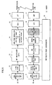
Fig.5 shows an embodiment of a modem using a method and an
apparatus for time equalization according to the present invention.
In this modem 10, a transmission system has an arrangement in
which a code converter 11, a signal point generator 12, a DMT
multiplexer (IFFT) 13, an amplitude modulator 14, a D/A converter 15,
and a low-pass filter (LPF) 16 are connected in series in this order.
Also, a reception system has an arrangement in which a
band-pass filter (BPF) 17, an A/D converter 18, a time equalizer 1, a
guard time remover 2, a DMT distributor (FFT) 3, a frequency
equalizer (FEQ) 4, a determining portion (DEC) 5, and a code inverter
6 are connected in series in this order. To each portion of this reception
system, a master frame signal is provided from a DMT master frame
synchronizer 19.
Firstly, as for the operation of the transmission system, scramble
processing (SCR), a serial (S)/parallel (P) conversion, a gray
(G)/natural (N) code conversion, and a sum calculation are performed
to a transmission signal SD at the code converter 11. Then, the signal
is outputted by the signal point generator 12 as a transmission signal
having sample points of a Nyquist interval (12 kB) as shown in Fig.2.
At the DMT multiplexer 13, the output signal from the signal
point generator 12 is multiplexed, by an inverse FFT (IFFT)
calculation, into a transmission signal as shown in Fig.3(2) between
the master frames shown in Fig.3(1).
At the amplitude modulator 14, a guard time is added to each
sub-frame of this multiplexed signal as shown in Fig.3(3) (as well as
Figs.8(1) and 8(2) described later), and two reference points R1 and R2
including zero-points for performing an amplitude modulation are
added to a DMT multiplexed signal (each DMT signal is composed of a
DMT signal of 16 symbols = channels), as shown in Fig.3(4).
One reference point R1 is (1+j0), and the other reference point
R2 is (0+j0). By using these reference points, the amplitude
modulation is performed. Timing phase information is extracted from
both reference points. A carrier amplitude and a carrier phase are
extracted by using the former reference point R1 (for a single
sub-frame). Accordingly, since the time equalization and the frequency
equalization can be realized by two sub-frames, the long training
signal becomes unnecessary.
The output signal of this amplitude modulator 14 is converted
into an analog signal at the D/A converter 15. At the low-pass filter 16,
a signal only in a low frequency band including a frequency band
(10-450 kHz) of a power carrier wave, for example, is extracted to be
provided to a transmission line.
As for the operation of the reception system, only a
predetermined frequency band component (10-450 kHz for power
carrier modem) is extracted from the signal received from the
reception line by the band-pass filter 17 to be restored to a digital
signal at the A/D converter 18.
Hereafter, the received signal is transmitted to the time
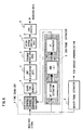
equalizer 1. An embodiment of this time equalizer 1 is shown in Fig.6.
This embodiment is composed of a timing phase controller 7 for
inputting the received signal from the A/D converter 18, and a
sub-frame extractor 8 for extracting timing phase information
from the received signal to be provided to the timing phase controller
7.
The sub-frame extractor 8 is further composed of a 90° section
extractor 81, a power calculator (PWR) 82, and a extractor 83. It is
to be noted that a master frame extractor 9 extracts a master frame
from the received signal to be provided to the DMT master frame
synchronizer 19 shown in Fig.5 for use in various synchronizing
signal.
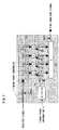
Also, for the timing phase controller 7 shown in Fig.6, as shown
in Fig.7, a transversal filter known as e.g. Japanese Patent
Application Laid-open No.10-224271 can be used, which is composed
of a delay circuit 71 for delaying the received signal at intervals of
sample points, a multiplication circuit 72 for multiplying the output
signal from the delay circuit 71 by coefficients C1-Cn, an addition
circuit 73 for adding the output signal of the multiplication circuit 72,
and a converter 74 composed of e.g. a table for converting the timing
phase information from the sub-frame extractor 8 into the
above-mentioned coefficients C1-Cn.
The operation of this time equalizer 1 will now be described
referring to Figs.8-10.
Firstly, when the reference points R1 and R2 inserted into two
sub-frames as shown in Figs.8(1) and 8(2) are received in the state
where the amplitude modulation of a modulation rate 100 % is applied
as shown in Fig.8(3), and when two sub-frames in combination are
supposed to form 360°, the 90° section extractor 81 in the sub-frame
extractor 8 cuts 90° sections at 90° intervals, as shown in
Figs.8(4)-8(7), to be provided to the power calculator 82.
Since the power calculation is performed to the 90° section only
at the reference point R1 in the power calculator 82 in case of Fig.8(4),
its integrated average is "1". When the power calculation section is
shifted by 90°, as shown in Fig.8(5), the integrated average is "1"
similarly. When the power calculation section is further shifted by 90°
in Fig.8(6), the power calculation is performed to the 90° section half
of which is at the reference point R1 and the other half of which is at
the reference point R2, thereby the integrated average assuming "0.5".
When the power calculation section is further shifted by 90°, the
power calculation is performed only within the reference point R2 as
shown in Fig.8(7), so that the integrated average assumes "0".
Since the calculation result of this power calculator 82 is a scalar,
adjoining integrated averages are added for vectorization. As a result,
if the power integrated averages of Figs.8(4) and 8(5) are vectorized,
the vector assumes (1+j1) as shown on the right side of Figs.8(4) and
8(5). Similarly, in case of Figs.8(5) and 8(6), it assumes (1+j0.5), and in
case of Figs.8(6) and 8(7), it is outputted as (0.5+j0).
Thus, with the power calculations continued, the
above-mentioned addition result is rotated about an origin O as a
vector signal as shown in Fig.8. A line L connecting the origin or a
center point O to a point (0+j0) at this time is a reference line, and an
angle ' for this line is provided to the extractor 83 shown in Fig.9
as a vector signal. The received signal is subject to a timing phase
control in accordance with the reference line L.
Thus, by calculating and integrating respective power of the
received signals whose time axes are different from each other, the
timing phase (reference point phase) of the received signals can be
obtained. If a time equalization is performed accordingly, DMT signals
of 16 channels are multiplexed into sub-frames in the DMT
multiplexed signal, so that the arrival times of channels coincide with
each other as shown in Fig.1(3).
The extractor 83 is composed of a multiplication circuit 83a, a
sign decision portion 83b, an addition circuit 83c, a delay circuit 83d,
and a vector signal generator 83e. Firstly, at the multiplication portion
83a, the vector signal ' is multiplied by another vector signal having
phase information of radius = 1.0 generated at the vector signal
generator 83e.
Then, the vector signal ' takes a phase rotation of Δ, and the
multiplication circuit 83a extracts only an imaginary component from
this signal to be transmitted to the sign decision portion 83b.
If the sign of this imaginary signal is +, the sign decision portion
83b outputs [FFFF]. If the sign is -, the sign decision portion 83b
outputs [0001] as the decision result to be provided to the adder 83b.
At the addition circuit 83c, the phase information previously sampled
through the delay circuit 83d is added thereto, so that a new phase
information is provided.
Since an integration circuit is composed of the addition circuit
83c and the delay circuit 83d, when the integrated value is
transmitted to the vector signal generator 83e, the vector signal
generator 83e performs a cos/sin conversion, converts a scalar input
into a vector output , and provides information of radius =1.0 to the
multiplication circuit 83a.
By repeating such an operation a plurality of times until the next
vector signal ' is inputted, a complex conjugate value
(corresponding to an amended amount of ') of the vector signal '
can be outputted from the delay circuit 83d as the timing phase
information.
It is to be noted that this operation is performed within two
sub-frames having the reference points R1 and R2 shown in Fig.8, and
the timing phase information is outputted every time the vector
signal ' is provided to the extractor 83, thereby enabling the timing
phase information to be sufficiently pulled in. Accordingly, a long
training signal is not required.
Also, in embodiment of the sign decision portion 83b shown in
Fig.9, a fixed decision result is outputted at all times depending on +
or -. However, by changing this decision result, much faster pull-in
can be achieved.
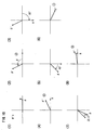
Namely, since a vector signal of the vector signal generator
83e is originally a reference vector R (1+j0) made by shifting the point
(0+j0) of the reference line L shown in Fig.8 to a point (-0.5+j0.5) and
by rotating the resultant by 135° , is coincident with the reference
vector R (1+j0) as shown in Fig.10(1). Since the vector signal '
coming into the multiplication circuit 83a is not rotated by the
multiplication circuit 83a at this time, the input signal of the sign
decision portion 83b remains as ', so that as shown in Fig.10(2), this
' is +.
The sign decision portion 83b, as shown in Fig.10(3), outputs the
decision result for rotating by 90° in the direction of -
(clockwise), so that the vector signal ' is rotated by 90° in the
direction of - as shown in Fig.10(4) to be brought near to the
reference point R.
Since the vector signal ' is still + in this state, the vector signal
is further rotated by 45° in the direction of - as shown in Fig.10(5),
and the vector ' now assumes - as shown in Fig.10(6).
If the vector signal is further rotated by 22.5° in the direction
of + as shown in Fig.10(7), the vector signal ' is brought nearer to
the reference point R as shown in Fig.10(8).
Thus, by the decision angle being halved in such an order of ±
90° →±45° →±22.5° →±11.25° →···, much faster timing phase
pull-in can be realized.
In the example of Fig.10, the integrated value of the timing
phase information = -90° , -45°, +22.5° , +11.25° , + ··· can
be obtained.
Supposing that the extractor 83 is composed of a DSP
(Digital Signal Processor) in this case, the value which the DSP can
obtain for an angle of ±180° is usually ±2.0. Therefore, the value
outputted from the sign decision portion 83b is indicated by two's
complement number as follows:
+2.0 → +180°
+1.0 → + 90°
+0.5 → + 45°
0.0 → 0°
-1.0 → -90°
-2.0 → -180°
The timing phase information thus obtained is provided to the
timing phase controller 7 shown in Fig.6. The timing phase controller
7, as shown in Fig.7, converts the timing phase information into
coefficients C1-Cn at the converter 74, which are provided to the
multiplication circuit 72. The multiplication circuit 72 multiples the
sampling outputs from the delay circuit 71 by coefficients C1-Cn.
Then, by mutually adding the multiplication results of the
multiplication portion 72 at the adder 73, a time-equalized signal can
be obtained. It is to be noted that this timing phase controller 7 can
output the time-equalized signal based on the timing phase
information by the above-mentioned known arrangement.
Hereafter, as shown in Fig.6, the time-equalized signal from the
timing phase controller 7 is transmitted to the guard time remover 2,
the DMT distributor 3, the frequency equalizer 4, the determining
portion 5, and the code inverter 6. This operation is the same as that
shown in Fig.15. Also, the frequency equalizer 4 performs a frequency
equalization only by using the reference point R1 shown in Fig.3(2).
Fig.11 shows a modification of the embodiment of the present
invention shown in Fig.6. While the FFT calculation is performed to
the time-equalized signal from the timing phase controller 7 at the
DMT distributor 3 through the guard time remover 2 in the
embodiment of Fig.6, the FFT calculation is divided into two in the
modification of Fig.11. Namely, the first FFT calculation is performed
at a DMT distributor 3a provided at a preceding stage of the timing
phase controller 7, and the second FFT calculation is performed at a
DMT distributor 3b provided at a subsequent stage.
Thus, since the FFT processing is performed once at the DMT
distributor 3a, a sampling frequency becomes low, which effects
enhancing the speed of calculation at the timing phase controller 7. It
is preferable that the guard time remover 2 is provided at the
preceding stage of the DMT distributor 3a in this case.
It is to be noted that while the guard time is added in the
above-mentioned description, a guard time period can be greatly
shortened by the time equalization according to the present invention
compared with an example of Fig.13, which does not block the
enhancement of the speed.
As described above, a method and an apparatus for time
equalization are arranged so that timing phase information is
extracted from a power spectrum of a received signal whose amplitude
is modulated per frame or sub-frame; and timing phase
synchronization of the received signal is performed with the timing
phase information. Therefore, the time equalization can be realized
without requiring a long training period
Also, it becomes possible to realize a much faster phase pull-in
by generating a vector signal of the power spectrum, by multiplying
the vector signal by another vector signal to be rotated, by performing
a sign decision of the rotated vector signal, by integrating a result of
the sign decision to be outputted as the timing phase signal, and by
performing a vector conversion of the integrated value to be fed back
as the other vector signal.